Article

Enhancement of Resistive and Synaptic Characteristics in Tantalum Oxide-Based RRAM by Nitrogen Doping

Division of Electronics and Electrical Engineering, Dongguk University, Seoul 04620, Korea
*
Author to whom correspondence should be addressed.
These authors contributed equally to this work.
Nanomaterials 2022, 12(19), 3334; https://doi.org/10.3390/nano12193334
Submission received: 6 September 2022 / Revised: 18 September 2022 / Accepted: 22 September 2022 / Published: 24 September 2022
(This article belongs to the Special Issue Redox-Based Resistive Nanomemristor for Neuromorphic Computing)

Abstract

:
Resistive random–access memory (RRAM) for neuromorphic systems has received significant attention because of its advantages, such as low power consumption, high–density structure, and high–speed switching. However, variability occurs because of the stochastic nature of conductive filaments (CFs), producing inaccurate results in neuromorphic systems. In this article, we fabricated nitrogen–doped tantalum oxide (TaOx:N)–based resistive switching (RS) memory. The TaOx:N–based device significantly enhanced the RS characteristics compared with a TaOx–based device in terms of resistance variability. It achieved lower device–to–device variability in both low-resistance state (LRS) and high–resistance state (HRS), 8.7% and 48.3% rather than undoped device of 35% and 60.7%. Furthermore, the N–doped device showed a centralized set distribution with a 9.4% variability, while the undoped device exhibited a wider distribution with a 17.2% variability. Concerning pulse endurance, nitrogen doping prevented durability from being degraded. Finally, for synaptic properties, the potentiation and depression of the TaOx:N–based device exhibited a more stable cycle–to–cycle variability of 4.9%, compared with only 13.7% for the TaOx–based device. The proposed nitrogen–doped device is more suitable for neuromorphic systems because, unlike the undoped device, uniformity of conductance can be obtained.

1. Introduction

New technologies such as artificial intelligence (AI) and the Internet of Things (IoT) are gaining attention, so rapid processing of vast amounts of data and information is required. However, in traditional digital computing—the von Neumann architecture—operation and storage devices are separated. Accordingly, bottlenecks occur when transferring complex data between devices [1,2]. Therefore, neuromorphic computing has emerged because of its parallel data processing with low power consumption and high-density structure. A neuromorphic system mimics a biological system—the human brain [3,4,5]. Recently, oxide–based device and resistance–based random–access memory designs, such as magnetic random–access memory (MRAM), ferroelectric random–access memory (FRAM), phase–change random–access memory (PRAM), spin–torque–transfer random–access memory (STT–RAM) and resistive random–access memory (RRAM) have been studied for implementation in neuromorphic systems [6,7,8]. RRAM is a promising candidate for the next generation of neuromorphic systems because of advantages such as high endurance, high–speed switching, low–power operation, scaling down capability, and multi–level cell (MLC) capability [9,10,11,12].
Despite these advantages, the filament–type RRAM cannot avoid large variations in conductance because the formation and rupture of filaments occur randomly, a drawback for use in neuromorphic systems [13]. Several studies have been reported to suppress the probabilistic nature of conducting filament formation, such as combining several oxide layers [14], semiconducting oxides [15,16], and doping techniques [17]. Nitrogen doping has been widely studied because it can control conductance accurately and effectively. Ref. [18] reported that N–doping in Ti/TiOx/Pt enhances the reliability effect on neuromorphic systems. Refs. [19,20,21,22,23] demonstrated that nitrogen doping in insulators can reduces the leakage path. Arikado, T et al., [24] stated that nitrogen eliminates oxygen vacancy related gap states by changing the charged states of Vo to Vo2+, so the leakage path can be reduced. Another important effect of nitrogen in the oxide layer is the restriction of oxygen ions’ diffusion. Y. E. Syu et al., [25] stated that, due to the higher bonding energy of N–O bond than the O–O bond, nitrogen can capture the oxygen atom to localize the oxygen ion near the conducting filament. Misha et al. [26] reported that incorporating nitrogen in TaOx improves uniformity at a low operating current. The performance of N–doped memory devices compared with undoped memory device in previous reports is summarized in Table 1.
In this study, the effect of nitrogen doping on synaptic properties and DC properties was also examined, in contrast with previous studies [26]. By incorporating nitrogen, smaller variations in DC endurance, AC endurance, device–to–device resistance, and set voltages are achieved compared with the undoped film. Furthermore, conductance is efficiently and gradually modulated by pulse–train measurement in the N–doped TaOx. Therefore, we investigated enhancing RS and synaptic properties in TaOx films with nitrogen doping.

2. Materials and Methods

The Ta/TaOx/Pt and Ta/TaOx:N/Pt devices were fabricated using the following process. First, we deposited the platinum (Pt) bottom electrode (BE) with a thickness of 100 nm using a thermal evaporator on a silicon oxide–silicon (SiO2/Si) substrate. The substrate was cleaned with acetone, isopropyl alcohol (IPA), and deionized (DI) water under ultra-sonication for 5 min each. The tantalum oxide (TaOx) and nitrogen–doped tantalum oxide (TaOx:N) switching layers were deposited with a thickness of 50 nm at room temperature. We applied a radiofrequency (RF) sputtering power of 240 W with the 3–inch tantalum metal target.
The pressure in the main chamber was maintained at 5 mTorr, and the gas flow rate was set to 20 sccm of Ar gas, 6 sccm of O2 gas, and an additional 1 sccm of N2 gas for the TaOx:N device. We then coated the negative PR and patterned it with a square pattern size of 100 μm. Then, the Ta top electrode (TE) was deposited by DC sputtering with a thickness of 100 nm.
Figure 1a demonstrates the cross–sectional transmission electron microscope (TEM, KANC, Suwon 16229, Republic of Korea) view and Figure 1b displays the distribution of the nitrogen doped insulator components (Ta, O, N) as indicated by EDS mapping. Figure 1b shows that the N content is uniformly distributed, indicating uniform and shallow N–doping on the TaOx films. Figure 1c illustrates the final patterned structure after the TE lift–off process. We examined the microstructure and thickness analysis of the memristor device. A semiconductor parameter analyzer (Keithly 4200–SCS and PMU ultrafast mode, Tektronix Inc., Beaverton, OR 97077, USA) was used to evaluate the device’s electrical characteristics.

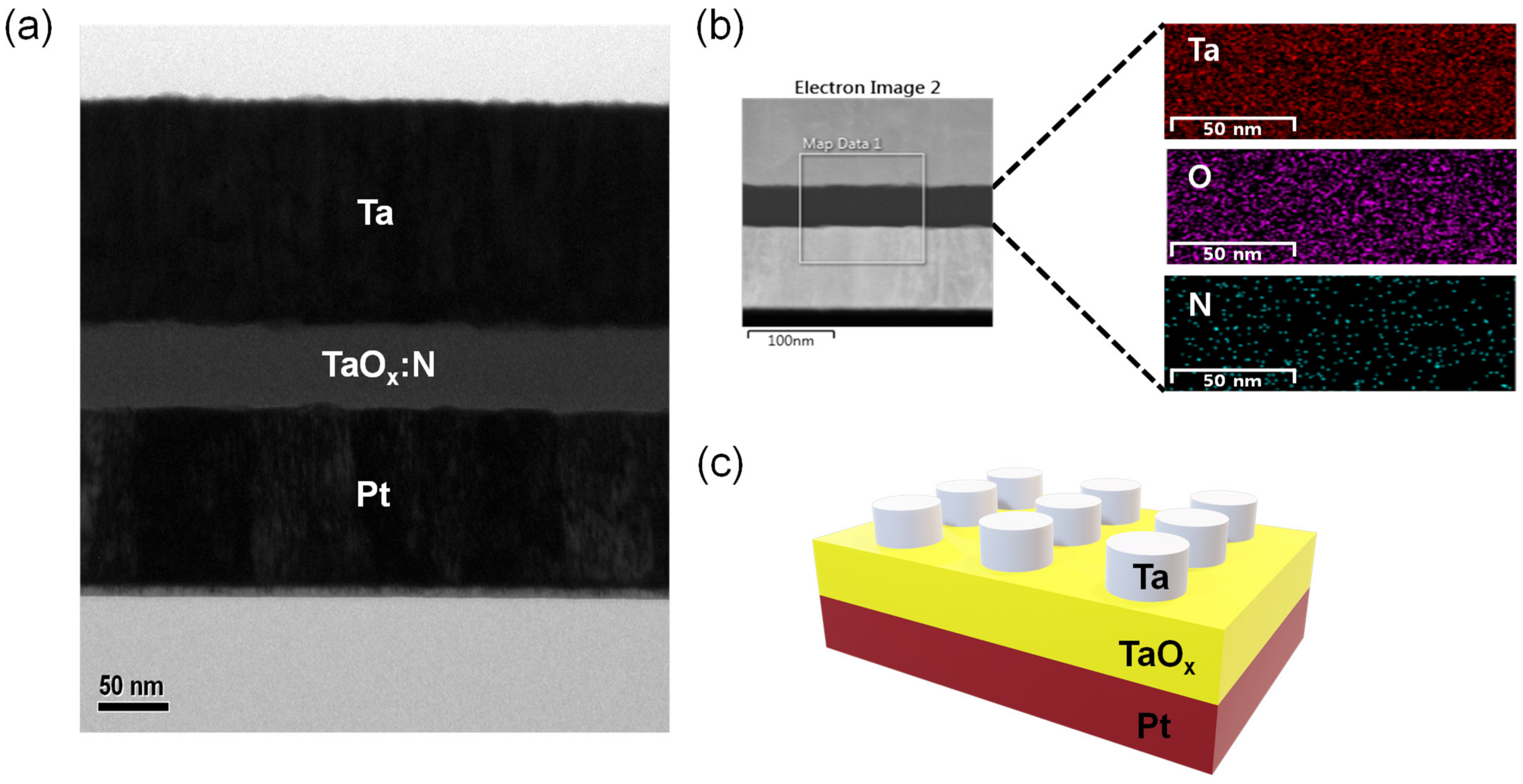
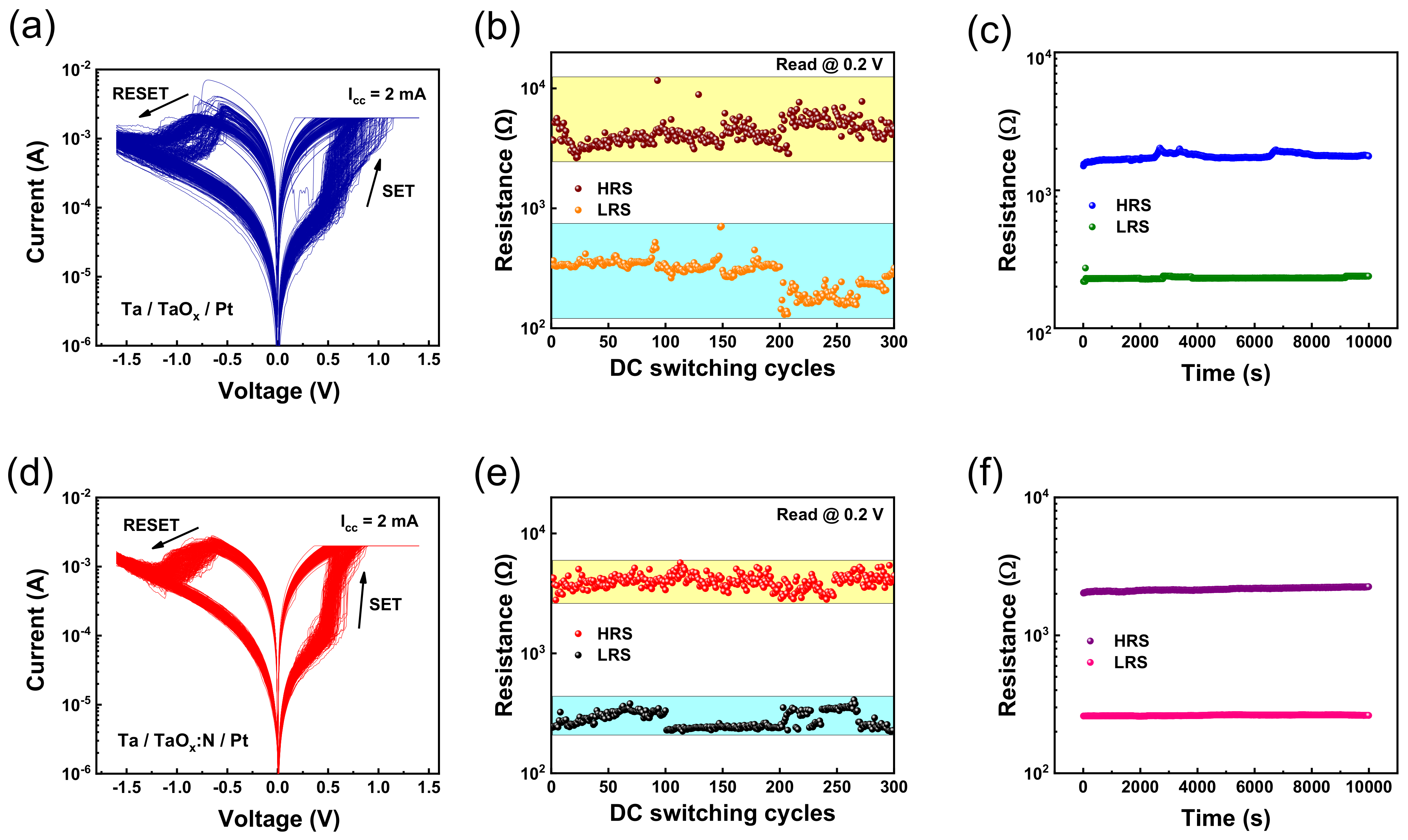
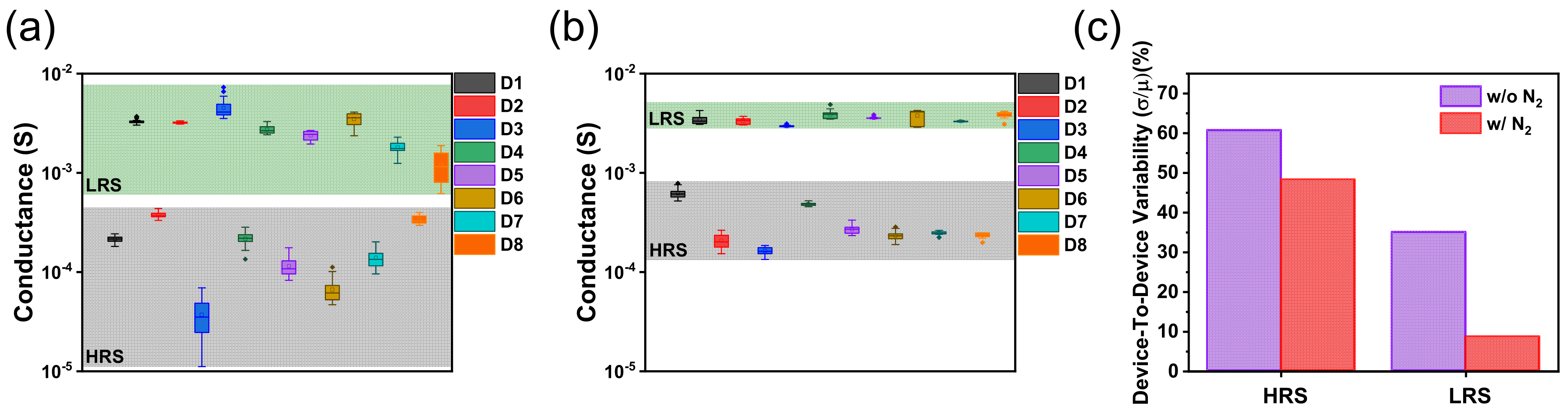
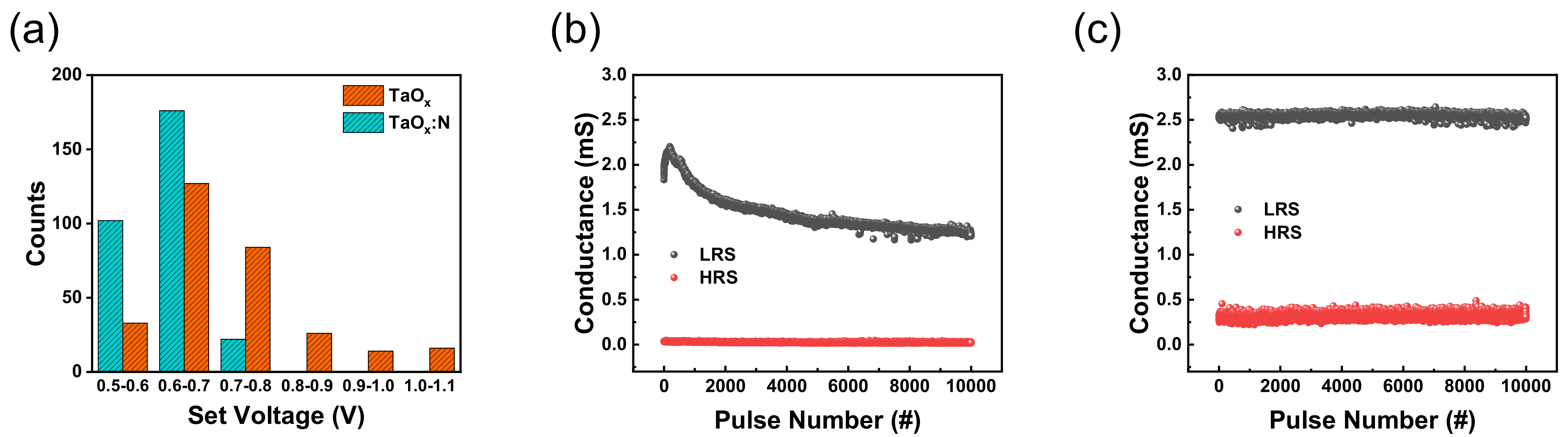
3. Results and Discussion

First, the electrical properties of the Ta/TaOx/Pt and Ta/TaOx:N/Pt memristors were measured. A preliminary forming process was required to produce a low–resistance state (LRS) from the initial state [27,28]. Both devices conducted 300 consecutive ON/OFF cycles by positive set and negative reset for the bipolar RS (BRS) after the forming process, as depicted in Figure 2a,d. Each memristor was measured under a compliance current of 2 mA in the set process with no current limit during reset switching to ensure a fair comparison. Furthermore, a negative voltage of −1.6 V was applied to switch from the LRS to the high–resistance state (HRS), and HRS changed to LRS under a positive voltage sweep from 0 to 1.4 V.
The detailed distribution of HRS and LRS values were extracted from the I−V characteristics measured at 0.2 V (Vread) during a cyclic test, as depicted in Figure 2b,e. The TaOx–based memristor exhibited a significant difference in resistance in the set and reset operations with cycle–to–cycle resistance variabilities (σ/μ) of 27.8% (LRS) and 23.7% (HRS). However, the TaOx:N–based memristor exhibited a stable RS characteristic with relatively small cycle–to–cycle resistance variabilities of 15.7% (LRS) and 13.2% (HRS). A retention characteristic test was performed to confirm the performance of the TaOx–based and TaOx:N–based memristors, as depicted in Figure 2c,f. Both devices can be maintained for 105 s without any degradation.
Eight randomly selected cells were assessed to confirm the device–to–device conductance uniformity. Uniformity is also to do with the size of the possible formed clusters, and the size of both devices is equal [29]. Each cell of both devices was applied by a voltage sweep in the range of 0 to −1.6 and 0 to 1.4 V for 20 cycles with a voltage step of 0.01 V, as presented in Figure 3a, b. For the TaOx–based device, the HRS ranges from 11.2 to 437 μS, and the LRS ranges from 0.62 to 7.3 mS (Figure 3a). In contrast, HRS values from 134 to 784 μS and LRS values from 3 to 4.9 mS are observed in the TaOx:N–based device (Figure 3b).
For the TaOx–based device, the range of conductance levels was wider than for the TaOx:N–based device. We used resistance variability to numerically identify the distribution of the HRS and LRS and accurately examine the extent to which data points differ. When the variability was calculated by considering only the average of LRS and HRS values in each cell, the device–to–device HRS variability decreased from 60.7 to 48.3%, and that of LRS decreased from 35 to 8.7% when nitrogen doping was applied, as illustrated in Figure 3c.
Furthermore, the set voltage distribution of both devices was characterized in histograms, as plotted in Figure 4a.
The uniformity of the set voltages is crucial to ensure error–free operation. Set voltage is the threshold where the resistance of the I−V curve abruptly decreases from HRS to LRS. As illustrated in Figure 4a, a wider set voltage distribution of the TaOx–based device is observed in the range of 0.5 to 1.1 V. In contrast, the TaOx:N–based device exhibits a more concentrated distribution in the range of 0.5 to 0.8 V. The statistical distribution of set voltages distribution is summarized in Table 2.
From the results of the DC characteristics, as described previously in Figure 2, Figure 3 and Figure 4, we confirmed that nitrogen doping on the TaOx–based device improved resistance variability and reliability—the most critical for ReRAM device applications [30].
Furthermore, a pulse endurance test was performed for up to 105 cycles to compare AC characteristics. A 10-μs pulse width of both set and reset pulses and amplitudes of 1.45 and −1.7 V were applied to both devices for a reliable comparison. The TaOx–based memristor exhibited unstable RS operation. Moreover, the conductance value in LRS degraded throughout the measurement, as presented in Figure 4b. In contrast, the TaOx:N–based memristor exhibited excellent endurance of up to 105 cycles.
Synaptic plasticity, such as long–term potentiation (LTP) and long–term depression (LTD), are crucial aspects of the application of neuromorphic systems [31]. The LTP and LTD were measured and discussed to compare the synaptic properties between the two devices. In Figure 5a,c, 100 potentiation and depression pulses were applied with 0.1 V read voltage pulses. The amplitude of potentiation and depression pulses were set to 0.9 and −1 V for the TaOx–based memristor and 0.94 and −1.05 V for the TaOx:N–based memristor. Moreover, the pulse width was fixed to 100 nS to ensure the pulse conditions were as similar as possible while modulating conductance gradually.
Ten cycles of potentiation and depression were conducted with these consecutive pulses. Figure 5b illustrates the degradation of the potentiation and depression during cycles of the undoped device. In contrast, Figure 5d illustrates a more constant and stable pulse measurement without degradation. When calculating the cycle–to–cycle resistance variability between the two devices, the nitrogen–doped device exhibited less variability of 4.9% compared with the 13.7% of the TaOx–based memristor.
Even for nitrogen–doped devices (4.9%), cycle–to–cycle variability occurred, as depicted in Figure 5. We reduced this variability by applying a DC set voltage to produce LRS. We then proceeded first with depression rather than potentiation, as depicted in Figure 6a,c. As depicted in Figure 6, 100 depression and potentiation pulses were applied with a 0.1 V read voltage pulse; ten cycles were conducted. The amplitudes of depression and potentiation pulses were set to −1.09 and 0.86 V for the TaOx–based memristor and −1 and 0.81 V for the TaOx:N–based memristor; the pulse width was set to 100 nS.
As depicted in Figure 6b, the cycle–to–cycle variation issue still occurred in the TaOx–based device. The conductance of the last point of a cycle does not match the first point of a subsequent cycle. In contrast, Figure 6d illustrates more stable synaptic properties, with a 2.1% cycle–to–cycle variability—a smaller value than when potentiation was performed first (4.9%). Based on these pulse measurement results (Figure 5 and Figure 6), device reliability is increased by incorporating nitrogen—similar to the DC measurement results. In biological neural networks, calculation and storage of information are performed simultaneously [32], so uniformity of resistance value is critical. Consequently, the TaOx:N–based memristor, which has higher cycle–to–cycle uniformity, is suitable for neuromorphic computing applications. Key performance indicators achieved in the present study are summarized in Table 3.

4. Conclusions

In this study, we investigated the role of nitrogen doping on resistive and synaptic characteristics while comparing the Ta/TaOx/Pt and Ta/TaOx:N/Pt devices. The TaOx:N–based memristor exhibited uniformity of resistance state and set voltages and a 105 pulse endurance. Furthermore, synaptic properties such as potentiation and depression were conducted with a pulse train. The TaOx:N–based memristor exhibited more stable conductance modulation when measuring potentiation first and depression first. In contrast, the TaOx–based memristor produces variability in the I–V curves, set voltages, and device-to-device resistance. It also degrades when pulse endurance, potentiation, and depression are measured. When we use RRAM as a neuromorphic system, the device should have low resistance variability. Therefore, a TaOx:N–based device is more suitable for an artificial synapse than an undoped–TaOx device.

Author Contributions

D.K. and J.K. wrote the manuscript; S.K. supervised the work. All authors have read and agreed to the published version of the manuscript.

Funding

This work was supported by the Korea Institute of Energy Technology Evaluation and Planning(KETEP) and the Ministry of Trade, Industry & Energy(MOTIE) of the Republic of Korea (No. 20224000000020) and was supported in part by a National Research Foundation of Korea (NRF) grant funded by the Ministry of Science (2021K1A3A1A49098073).

Institutional Review Board Statement

Not applicable.

Informed Consent Statement

Not applicable.

Data Availability Statement

Not applicable.

Conflicts of Interest

The authors declare no conflict of interest.

References

  1. Indiveri, G.; Liu, S.C. Memory and information processing in neuromorphic systems. Proc. IEEE 2015, 103, 1379–1397. [Google Scholar] [CrossRef]
  2. Nawrocki, R.A.; Voyles, R.M.; Shaheen, S.E. A mini review of neuromorphic architectures and implementations. IEEE Trans. Electron Devices 2019, 66, 4722–4726. [Google Scholar] [CrossRef]
  3. Kim, K.H.; Gaba, S.; Wheeler, D.; Cruz-Albrecht, J.M.; Hussain, T.; Srinivasa, N.; Lu, W. A functional hybrid memristor crossbar-array/CMOS system for data storage and neuromorphic applications. Nano Lett. 2012, 12, 389–395. [Google Scholar] [CrossRef] [PubMed]
  4. Jo, S.H.; Chang, T.; Ebong, I.; Bhadviya, B.B.; Mazumder, P.; Lu, W. Nanoscale memristor device as synapse in neuromorphic systems. Nano Lett. 2010, 10, 1297–1301. [Google Scholar] [CrossRef] [PubMed]
  5. Burr, G.W.; Shelby, R.M.; Sebastian, A.; Kim, S.; Kim, S.; Sidler, S.; Virwani, K.; Ishii, M.; Narayanan, P.; Fumarola, A.; et al. Neuromorphic computing using non-volatile memory. Adv. Phys. X 2017, 2, 89–124. [Google Scholar] [CrossRef]
  6. Martins, R.; Barquinha, P.; Pereira, L.; Correia, N.; Gonçalves, G.; Ferreira, I.; Fortunato, E. Selective floating gate non-volatile paper memory transistor. Phys. Status Solidi Rapid Res. Lett. 2009, 3, 308–310. [Google Scholar] [CrossRef]
  7. Wang, Z.; Wu, H.; Burr, G.W.; Hwang, C.S.; Wang, K.L.; Xia, Q.; Yang, J.J. Resistive switching materials for information processing. Nat. Rev. Mater. 2020, 5, 173–195. [Google Scholar] [CrossRef]
  8. Zhu, J.; Zhang, T.; Yang, Y.; Huang, R. A comprehensive review on emerging artificial neuromorphic devices. Appl. Phys. Rev. 2020, 7, 011312. [Google Scholar] [CrossRef]
  9. Ryu, H.; Kim, S. Self-Rectifying Resistive Switching and Short-Term Memory Characteristics in Pt/HfO2/TaOx/TiN Artificial Synaptic Device. Nanomaterials 2020, 10, 2159. [Google Scholar] [CrossRef] [PubMed]
  10. Ryu, H.; Kim, S. Synaptic characteristics from homogeneous resistive switching in Pt/Al2O3/TiN stack. Nanomaterials 2020, 10, 2055. [Google Scholar] [CrossRef] [PubMed]
  11. Ismail, M.; Chand, U.; Mahata, C.; Nebben, J.; Kim, S. Demonstration of synaptic and resistive switching characteristics in W/TiO2/HfO2/TaN memristor crossbar array for bioinspired neuromorphic computing. J. Mater. Sci. Technol. 2022, 96, 94–102. [Google Scholar] [CrossRef]
  12. Carlos, E.; Branquinho, R.; Martins, R.; Kiazadeh, A.; Fortunato, E. Recent progress in solution-based metal oxide resistive switching devices. Adv. Mater. Interfaces 2021, 33, 2004328. [Google Scholar] [CrossRef] [PubMed]
  13. Kim, S.; Abbas, Y.; Jeon, Y.R.; Sokolov, A.S.; Ku, B.; Choi, C. Engineering synaptic characteristics of TaOx/HfO2 bi-layered resistive switching device. Nanotechnology 2018, 29, 415204. [Google Scholar] [CrossRef]
  14. Ismail, M.; Abbas, H.; Mahata, C.; Choi, C.; Kim, S. Optimizing the thickness of Ta2O5 interfacial barrier layer to limit the oxidization of Ta ohmic interface and ZrO2 switching layer for multilevel data storage. J. Mater. Sci. Technol. 2022, 106, 98–107. [Google Scholar] [CrossRef]
  15. Simanjuntak, F.M.; Ohno, T.; Samukawa, S. Film-nanostructure-controlled inerasable-to-erasable switching transition in ZnO-based transparent memristor devices: Sputtering-pressure dependency. ACS. Appl. Electron. Mater. 2019, 1, 2184–2189. [Google Scholar] [CrossRef]
  16. Zhang, L.; Xu, Z.; Han, J.; Liu, L.; Ye, C.; Zhou, Y.; Xiong, W.; Liu, Y.; He, G. Resistive switching performance improvement of InGaZnO-based memory device by nitrogen plasma treatment. J. Mater. Sci. Technol. 2020, 49, 1–6. [Google Scholar] [CrossRef]
  17. Syu, Y.E.; Chang, T.C.; Tsai, T.M.; Chang, G.W.; Chang, K.C.; Tai, Y.H.; Tsai, M.-J.; Wang, Y.-L.; Sze, S.M. Silicon introduced effect on resistive switching characteristics of WOX thin films. Appl. Phys. Lett. 2012, 100, 022904. [Google Scholar] [CrossRef]
  18. Park, J.; Park, E.; Kim, S.; Yu, H.Y. Nitrogen-induced enhancement of synaptic weight reliability in titanium oxide-based resistive artificial synapse and demonstration of the reliability effect on the neuromorphic system. ACS Appl. Mater. Interfaces 2019, 11, 32178–32185. [Google Scholar] [CrossRef]
  19. Hong, S.M.; Kim, H.D.; Yun, M.J.; Park, J.H.; Jeon, D.S.; Kim, T.G. Improved resistive switching properties by nitrogen doping in tungsten oxide thin films. Thin Solid Films 2015, 583, 81–85. [Google Scholar] [CrossRef]
  20. Xu, J.; Zhu, Y.; Liu, Y.; Wang, H.; Zou, Z.; Ma, H.; Wu, X.; Xiong, R. Improved Performance of NbOx Resistive Switching Memory by In-Situ N Doping. Nanomaterials 2022, 12, 1029. [Google Scholar] [CrossRef]
  21. Xie, H.; Liu, Q.; Li, Y.; Lv, H.; Wang, M.; Liu, X.; Sun, H.; Yang, X.; Long, S.; Liu, S.; et al. Nitrogen-induced improvement of resistive switching uniformity in a HfO2-based RRAM device. Semicond. Sci. Technol. 2012, 27, 125008. [Google Scholar] [CrossRef]
  22. Wei, X.; Huang, H.; Ye, C.; Wei, W.; Zhou, H.; Chen, Y.; Zhang, R.; Zhang, L.; Xia, Q. Exploring the role of nitrogen incorporation in ZrO2 resistive switching film for enhancing the device performance. J. Alloy. Compd. 2019, 775, 1301–1306. [Google Scholar] [CrossRef]
  23. Yang, M.; Kamiya, K.; Shirakawa, H.; Magyari-Kope, B.; Nishi, Y.; Shiraishi, K. Role of nitrogen incorporation into Al2O3-based resistive random-access memory. Appl. Phys. Express 2014, 7, 074202. [Google Scholar] [CrossRef]
  24. Umezawa, N.; Shiraishi, K.; Ohno, T.; Watanabe, H.; Chikyow, T.; Torii, K.; Yamabe, K.; Yamada, K.; Kitajima, H.; Arikado, T. First-principles studies of the intrinsic effect of nitrogen atoms on reduction in gate leakage current through Hf-based high-k dielectrics. Appl. Phys. Lett. 2005, 86, 143507. [Google Scholar] [CrossRef]
  25. Syu, Y.E.; Zhang, R.; Chang, T.C.; Tsai, T.M.; Chang, K.C.; Lou, J.C.; Sze, S.M.; Young, T.-F.; Chen, J.-H.; Chen, M.-C.; et al. Endurance Improvement Technology With Nitrogen Implanted in the Interface of WSiOx Resistance Switching Device. IEEE Electron Device Lett. 2013, 34, 864–866. [Google Scholar] [CrossRef]
  26. Misha, S.H.; Tamanna, N.; Woo, J.; Lee, S.; Song, J.; Park, J.; Lim, S.; Hwang, H. Effect of nitrogen doping on variability of TaOx-RRAM for low-power 3-bit MLC applications. ECS Solid State Lett. 2015, 4, P25. [Google Scholar] [CrossRef]
  27. Bersuker, G.; Gilmer, D.C.; Veksler, D.; Kirsch, P.; Vandelli, L.; Padovani, A.; Larcher, L.; McKenna, K.; Shluger, A.; Iglesias, V.; et al. Metal oxide resistive memory switching mechanism based on conductive filament properties. J. Appl. Phys. 2011, 110, 124518. [Google Scholar] [CrossRef]
  28. Padovani, A.; Larcher, L.; Pirrotta, O.; Vandelli, L.; Bersuker, G. Microscopic modeling of HfOx RRAM operations: From forming to switching. IEEE Trans. Electron Devices 2015, 62, 1998–2006. [Google Scholar] [CrossRef]
  29. Rosa, J.; Kiazadeh, A.; Santos, L.; Deuermeier, J.; Martins, R.; Gomes, H.L.; Fortunato, E. Memristors using solution-based IGZO nanoparticles. ACS Omega 2017, 2, 8366–8372. [Google Scholar] [CrossRef]
  30. Kim, Y.; Choi, H.; Park, H.S.; Kang, M.S.; Shin, K.Y.; Lee, S.S.; Park, J.H. Reliable multistate data storage with low power consumption by selective oxidation of pyramid-structured resistive memory. ACS Appl. Mater. Interfaces 2017, 9, 38643–38650. [Google Scholar] [CrossRef]
  31. Yu, S. Neuro-inspired computing with emerging nonvolatile memorys. Proc. IEEE 2018, 106, 260–285. [Google Scholar] [CrossRef]
  32. Furber, S. Large-scale neuromorphic computing systems. J. Neural Eng. 2016, 13, 051001. [Google Scholar] [CrossRef] [PubMed]
Figure 1. (a) High magnification imaged by TEM. (b) Overall image for EDS mapping. (c) Schematic displaying the device structure.
Nanomaterials 12 03334 g001
Figure 2. RS characteristics of Ta/TaOx/Pt device: (a) I−V curves of 300 consecutive switching cycles, (b) LRS and HRS state resistance distribution for each cycle at 0.2 V (c) Retention characteristics test for LRS and HRS. RS characteristics of Ta/TaOx:N/Pt device: (d) I−V curves of 300 repetitive switching cycles, (e) LRS and HRS state resistance measurement for each cycle at 0.2 V (f) Retention characteristics test for LRS and HRS.
Nanomaterials 12 03334 g002
Figure 3. HRS and LRS distributions of eight randomly selected memory cells of (a) Ta/TaOx/Pt device and (b) Ta/TaOx:N/Pt device. (c) Device–to–device variation for two devices.
Nanomaterials 12 03334 g003
Figure 4. (a) Statistical distribution of set voltages for Ta/TaOx/Pt and Ta/TaOx:N/Pt. Pulse endurance characteristics of (b) Ta/TaOx/Pt device and (c) Ta/TaOx:N/Pt device.
Nanomaterials 12 03334 g004
Figure 5. Ta/TaOx/Pt device: (a) LTP and LTD are established with 100 identical write pulses (amplitudes of 0.9 V, the pulse width of 100 ns) and erase pulses (amplitudes of −1 V, the pulse width of 100 ns) (b) Ten cycles of potentiation and depression (potentiation first). Ta/TaOx:N/Pt device: (c) LTP and LTD are established with 100 identical write pulses (amplitudes of 0.94 V, the pulse width of 100 ns) and erase pulses (amplitudes of −1.05 V, the pulse width of 100 ns) (d) Ten cycles of potentiation and depression (potentiation first).
Nanomaterials 12 03334 g005
Figure 6. Ta/TaOx/Pt device: (a) LTD and LTP are established with 100 identical erase pulses (amplitudes of −1.09 V, the pulse width of 100 ns) and write pulses (amplitudes of 0.86 V, the pulse width of 100 ns) (b) Ten cycles of depression and potentiation (depression first). Ta/TaOx:N/Pt device: (c) LTD and LTP are established with 100 identical erase pulses (amplitudes of −1 V, the pulse width of 100 ns) and write pulses (amplitudes of 0.81 V, the pulse width of 100 ns) (d) Ten cycles of depression and potentiation (depression first).
Nanomaterials 12 03334 g006
Table 1. Performance of N–doped Memory Devices Compared with Undoped Memory Device in Previous Reports.
DeviceDopingOn/Off RatioVset (V)Retention (s)MNISTRef
Pt/NbOx/PtUndoped~101.3–1.94 × 103N.A.[20]
N–doped~1030.4–1.36 × 10⁴N.A.
Ti/WOx/PtUndoped~10N.A.102N.A.[19]
N–doped~102N.A.104N.A.
Ti/TiOx/PtUndoped-Not uniform10321.1%[18]
N–doped-uniform10564.4%
Table 2. Statistical Distribution of Set Voltages Obtained With 300 DC Switching Cycles.
Vset (V)
DeviceΜσσ∕μ
Undoped0.720.1217.2%
N–doped0.620.0599.4%
Table 3. Key Performance Indicators Achieved in The Present Study.
DeviceCycle-to-Cycle
Variability (LRS, HRS)
RetentionDevice-to-Device
Variability (LRS, HRS)
Vset
Variability
Pulse
Endurance
LTP, LTD
Variability
Undoped(27.8%, 23.7%)~104 s(35%, 60.7%)17.2%-degradation4.9%
N–doped(15.7%, 13.2%)~104 s (8.7%, 48.3%)9.4%~10513.7%
Publisher’s Note: MDPI stays neutral with regard to jurisdictional claims in published maps and institutional affiliations.

