Review

Evolution Application of Two-Dimensional MoS2-Based Field-Effect Transistors

1
School of Science, Xi’an Polytechnic University, Xi’an 710048, China
2
Guangxi Key Laboratory of Processing for Nonferrous Metals and Featured Material, School of Resources, Environment and Materials, Guangxi University, Nanning 530004, China
*
Author to whom correspondence should be addressed.
Nanomaterials 2022, 12(18), 3233; https://doi.org/10.3390/nano12183233
Submission received: 21 August 2022 / Revised: 12 September 2022 / Accepted: 15 September 2022 / Published: 18 September 2022

Abstract

:
High-performance and low-power field-effect transistors (FETs) are the basis of integrated circuit fields, which undoubtedly require researchers to find better film channel layer materials and improve device structure technology. MoS2 has recently shown a special two-dimensional (2D) structure and superior photoelectric performance, and it has shown new potential for next-generation electronics. However, the natural atomic layer thickness and large specific surface area of MoS2 make the contact interface and dielectric interface have a great influence on the performance of MoS2 FET. Thus, we focus on its main performance improvement strategies, including optimizing the contact behavior, regulating the conductive channel, and rationalizing the dielectric layer. On this basis, we summarize the applications of 2D MoS2 FETs in key and emerging fields, specifically involving logic, RF circuits, optoelectronic devices, biosensors, piezoelectric devices, and synaptic transistors. As a whole, we discuss the state-of-the-art, key merits, and limitations of each of these 2D MoS2-based FET systems, and prospects in the future.

1. Introduction

The FET is voltage-adjustable electronic device that controls the output circuit current by controlling the electric field effect of the input circuit, which can work at very low current and voltage, and which can easily integrate on a piece of silicon and other substrates, so the FET has been widely used in large-scale integrated circuits [1]. The common FET device structure consists of a gate, source/drain, channel layer and dielectric. As is well known, the continuous miniaturization of silicon (Si)-based FETs has driven the exponential growth of integrated circuits for more than half a century. However, with the bulk thickness reduced to less than 10 nm, Si FETs exhibit a large number of attenuation phenomena of carrier mobility. This requires researchers to come up with a series of strategies to overcome this limitation, such as finding new materials, developing new structures, and improving processes [1,2].
Recently, 2D materials including graphene [3], black phosphorus (BP) [4], and transition metal dichalcogenides (TMDs) [5,6,7,8] have shown natural advantages for the further reduction in FET sizes due to their natural atomic-level thickness and surface without hanging bonds, for remedying the shortcomings of Si-based FETs. Table 1 summarizes the main electric performance of MoS2-based FETs and other mainstream 2D materials-based FETs. The graphene FET has ultra-high mobility. However, its Ion/Ioff ratio is lowest (typical below 10) owing to the lack of bandgap, and it is difficult to apply to logic electronics. The mobility of the BP FET is much higher than that of the MoS2 FET, but it is not stable, due to reaction with water and oxygen in the air to decompose. TMDs (MoS2, WS2, WSe2, etc.)-based FETs have an ultrahigh Ion/Ioff ratio and good mobility, which can be assembled into low-power electronics. Especially, MoS2 FETs have the advantages of higher mobility, higher Ion/Ioff ratio, and lower subthreshold swing, compared with other TMD FETs. Overall, MoS2 is the most suitable channel layer material for FETs, and MoS2 FETs are the promising candidate for downscaling electronics with a short channel, low thickness, small volume, fast speed, high sensitivity, light weight, etc.
Table 1 also shows that different MoS2 FETs have performed differently, because the natural atomic-level thickness and large specific surface area of MoS2 make the interface quality have a great influence on the MoS2 properties [2]. High-quality MoS2 preparation methods have constantly been investigated in recent years. The common preparation methods of MoS2 include Chemical Vapor Deposition (CVD), Metal–Organic Chemical Vapor Deposition (MOCVD), Atomic-layer deposition (ALD), and Vapor–Liquid–Solid (VLS) [18]. The properties of stripped MoS2 are better than those of CVD-prepared MoS2, because stripped MoS2 has high quality and less impurities, while the CVD process will bring a lot of impurities. In addition, a 6-inch uniform monolayer MoS2 can be grown by CVD in a short time [19]. MoS2 with the low surface energy can also be easily stripped and transferred, the size of which depends mainly on the size of the bulk MoS2, which can reach the centimeter level [20].
However, in MoS2 FETs, a high-quality MoS2 between the contact electrode and the dielectric layer will still be obtained at the contact interface and dielectric interface, which has further led to the different performance of MoS2 FETs [21]. Therefore, for improving the performance of MoS2 FETs, we mainly focus on optimizing the contact behavior [14], regulating the conductive channel [16], and rationalizing the dielectric layer [17]. This is also the subject of our review. Then, we discuss the applications of MoS2 FETs in key and emerging fields [21], involving logic and RF circuits [22,23], optoelectronic devices [24], biosensors [25], piezoelectric devices [26], and synaptic transistors [27] (Figure 1).

2. Performance Improvement Strategy of MoS2 FETs

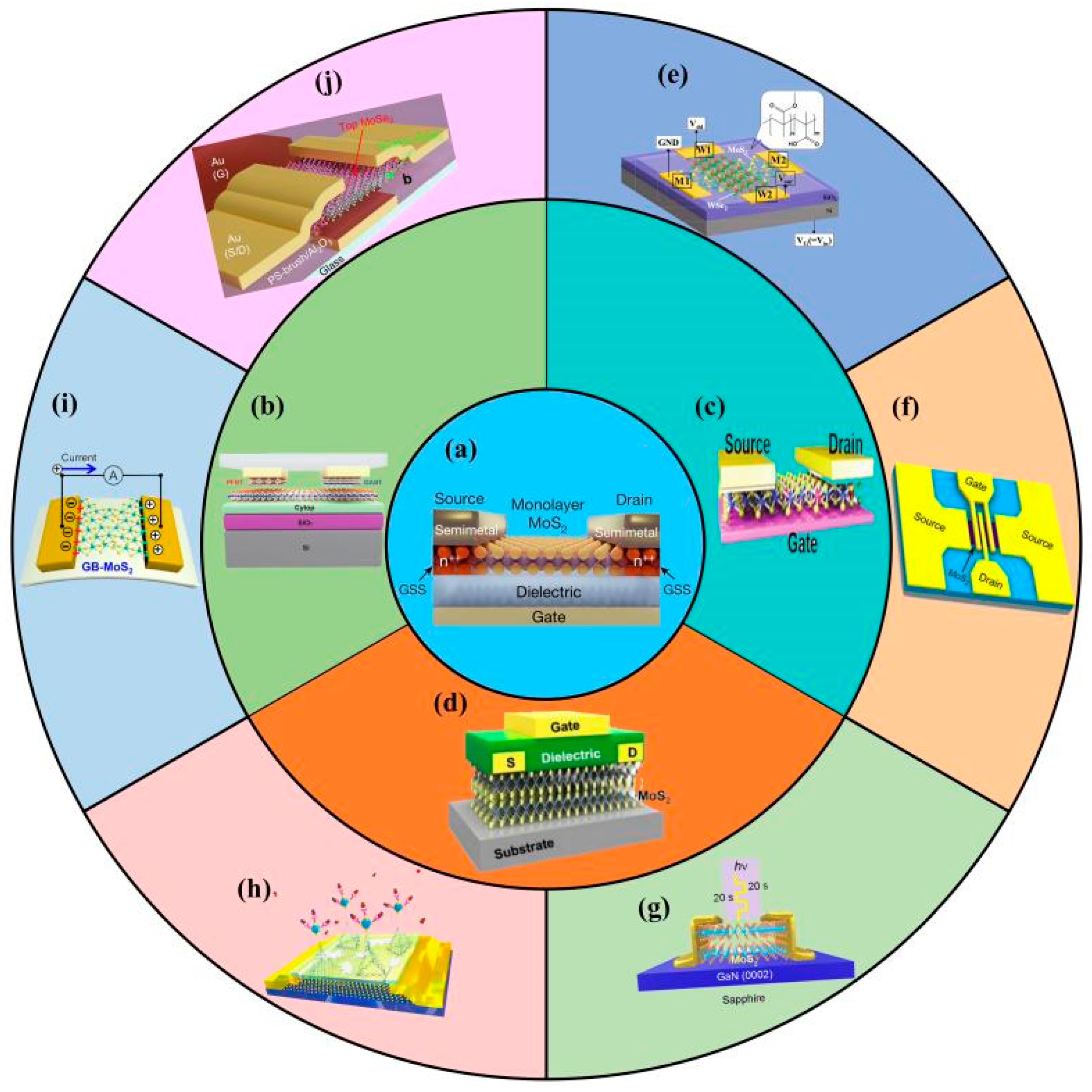
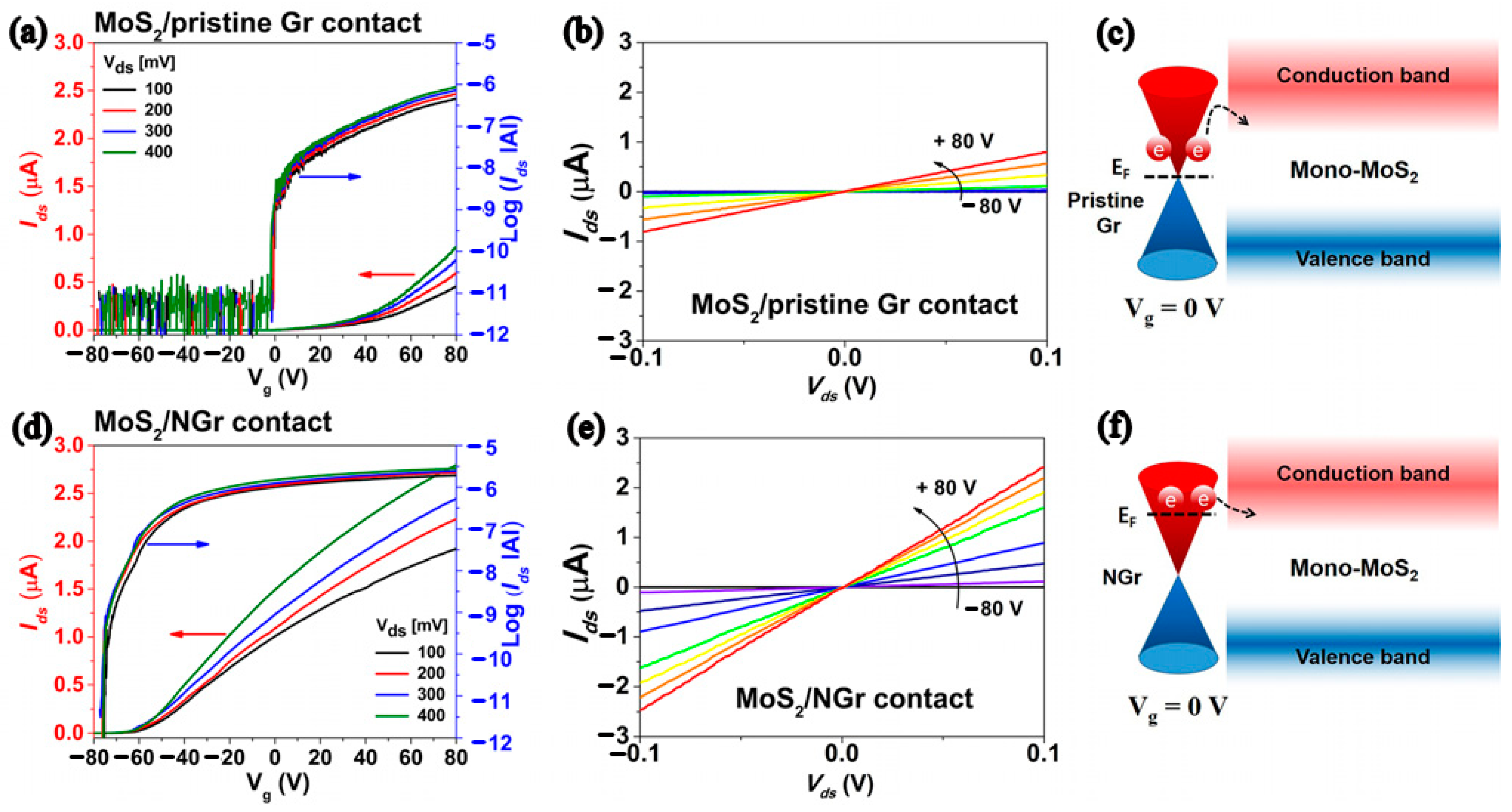
2.1. Optimizing Contact Behavior

A metal electrode and traditional 2D electrode are usually directly deposited by chemical or physical deposition methods on MoS2 surfaces, which damages the contact interface, resulting in the Schottky barrier and Fermi-level pinning effect, between the MoS2/metal electrode, and the MoS2/traditional 2D semiconductor in MoS2 FETs [28], which could reduce electrical performance [29]. Therefore, it is very important to find suitable electrode materials to form ohmic contact and eliminate the Fermi pinning effect [30]. Recently, the van der Waals contact has been an indirect method of preparation into MoS2, which does not use direct chemical bonding, avoiding the damage of the deposition process and the diffusion at the contact interface, Here, we review the methods for obtaining ultra-low contact resistance in both 2D and non-2D contacts.
Shen et al. prepared a back-gated monolayer MoS2 FET, where bismuth, nickel, and titanium were used as electrodes to explore the contact barrier. The results showed that the Bi-MoS2 FET had the lowest contact barrier (123 Ω μm at a carrier density of 1.5 × 1013 cm−2), attributed to the suppression of metal-induced interstitial states by the semi-metallic bismuth contact with MoS2. This mechanism also contributes to good ohmic contact in other TMDs FETs, i.e., the Ion/Ioff ratios are as high as (107) at low voltages (1.5 V) [21].
Samori et al. prepared an asymmetric Schottky diode by self-assembled monolayers (SAMs) of pre-functionalized gold electrodes, then transferring them to MoS2 by the dry method [14]. Figure 2a shows the MoS2 FETs structure, where the drain/source electrodes are 2, 3, 4, 5, 6-pentafluorobenzenethiol (PFBT)-functionalized electrodes and the source 4-(dimethylamine) benzenethiol (DABT) functionalized electrode, respectively. The output curve of the Schottky diode is shown in Figure 2b. The Vgs of the device is reduced from 90 to −30 V, and the rectification ratio reaches a maximum of 103 at −30 V in Figure 2c. Figure 2d–f show the band structure of devices under different bias voltages. This strategy can be adjusted to control the electrode and different chemisorption SAMs functionalization to reduce (increase) the charge injection barrier, thus providing a strategy for the manufacture of asymmetric charge injection devices [14].
Recently, experiments have found that graphene materials as the electrodes of MoS2 FETs can also achieve good ohmic characteristics [31]. Yu et al. fabricated graphene/MoS2 heterojunction FETs, by adjusting the Fermi level of the graphene electrode to modulate the height of the Schottky barrier between heterojunctions, where the short-channel effect with a channel length less than 30 nm was successfully eliminated, and at the same time, the drain-induced barrier lowering of the device was 0.92 v/v and the Ion/Ioff ratio was as high as 108 [31]. Kim et al. reported high properties of monolayer MoS2 FETs with a nitrogen-doped graphene (NGr) electrode [15], as shown in Figure 3. Compared to undoped graphene electrodes, the device current increased 214% and the field-effect mobility increased fourfold. Figure 3c,f illustrates that the Fermi level of MoS2 FET was improved by employing the NGr electrode. Therefore, this is one of the effective means to reduce contact resistance, which will provide a new idea for the development of high-performance devices.
Two-dimensional Mxenes contain transition metal carbides, carbonitrides, and nitrides, and have graphene-like surface structures and good electrical conductivity [32], which show great application potential in barriers, capacitors, and electrodes of electrochemical systems [33]. Dai et al. calculated the contact barrier of MoS2 FETs with Ta2C, Ta2CF2, and Ta2C(OH)2 as the electrode material, using density functional theory. The results showed that the N-type Schottky barrier was created by a Ta2C electrode. However, using a Ta2CF2 or Ta2C(OH)2 electrode can form ohmic contact, and the resistance of MoS2/Ta2C(OH)2 was 2 times smaller than that of MoS2/Ta2CF2. This study provides theoretical guidance for the application of MXene materials in MoS2 FETs [30]. Du et al. first studied the contact characteristics between MoS2 and M3C2(OH)2 (M = Ti, Zr, Hf) by first principles, which found that Ti and Hf are more suitable for ohmic contact as electrode materials. The subthreshold swing (SS) range of devices was 100~200 mV/decade, and the Ion/Ioff ratio was as high as 106, in the sub-10 nm range [34].
To sum up, in the modification of the MoS2 FET electrode, the selection of an appropriate metal electrode or other excellent electrode materials can reduce the Schottky barrier, especially the combination of the above new two-dimensional material, and MoS2 can better achieve a high-performance, low-power-consumption FET, which will also be a significant attraction for the development of electronic devices in the future. In addition, 2D MoS2 could produce unique quantum effects by contacting with the metal, such as quantum transport, superconductors, and valley transport [35].

2.2. Boosting Conductive Channel

MoS2 with the good direct bandgap (~1.8 eV) when the bulk MoS2 is stripped to monolayer MoS2 sets the stage for MoS2 FETs with high mobility and high Ion/Ioff ratio [36]. As is well known, doping is one of the most prevalent techniques to regulate the band structure of semiconductor materials [37], which have both metal ion doping and nonmetal ion doping. An oxygen uniformly doped monolayer MoS2 can be prepared directly by in situ chemical vapor deposition on a 2-inch sapphire substrate. The results showed that the bandgap of MoS2 was regulated (from 2.25 eV (intrinsic) to 1.72 eV (heavily doped). The mobility of the MoS2-XOx FET was 78 cm2/Vs, and the Ion/Ioff ratio was 3.5 × 10⁸ [38]. Shi et al. developed a one-step CVD method to achieve the growth of centimeter-level monolayer MoS2 film [16]. Unidirectionally Fe-doped MoS2 domains (domain size up to 250 µm) were prepared on 2-inch commercial c-plane sapphire, which achieved very low contact resistance (≈678 Ω µm) and good ohmic contact with the electrode, as shown in Figure 4a–c. MoS2 FETs obtained electron mobility (54 cm2V−1s−1 at room temperature, 94 cm2/Vs at 100 K, and Ion/Ioff ratio (108)). The electron mobility of monolayer Fe-MoS2 was decreased with increasing temperature, as observed in Figure 4d,e, which indicated that it can inhibit the scattering of impurities. Figure 4f shows the energy barriers of pristine MoS2 and Fe-MoS2.
Wang et al. first synthesized a Ta-doped p-type monolayer MoS2 by NaCl-assisted CVD, which has the advantages of large area, controllability, high quality, and controllable doping concentration [39]. With the addition of Ta, MoS2 FET devices showed bipolar properties and changed from N type to P type with increasing concentration. The p-type MoS2 active layer was applied with heavy niobium doping by mechanical stripping on the Si substrate. Then, the p-type MoS2 FETs with the Pt electrode obtained a 0.13 eV contact barrier, output current of −10 µA, and drain voltage of −1 V when the channel length was ~1 µm [40]. Han et al. reported a strategy for the controllable transformation of n-type MoS2 into p-type MoS2 by low energy (100 eV) He+ irradiation, as shown in Figure 5. Through theoretical calculation and characterization, it was found that this method increases the band size through the migration of the topmost S atom, and electron capture transforms n-type MoS2 into p-type MoS2 [41].
Doping can effectively improve the performance of MoS2 films, but in the case of thin atom thickness or few layers, traditional doping strategies such as ion implantation or high-temperature diffusion could not improve the performance, because these methods tend to destroy the lattice and produce defects. Therefore, it is particularly important to find new doping methods, which provides inspiration for future research and development of more processes suitable for less layer MoS2 doping.

2.3. Rationalizing Dielectric Layer

As for the MoS2 FET, the surface accumulation of charges and charge traps on the dielectric are big issues leading to high leakage current, which is observed by using a scanning tunneling microscope [42,43]. Therefore, an appropriate dielectric layer with high permittivity should be used to effectively reduce the influence of impurity scattering at the interface on carrier transport in the channel layer, while avoiding the possible short-channel effect and reducing gate leakage current [44,45]. It is noted that a high-K dielectric layer (HfO2, ZrO2, HfZrO, etc.) can effectively shield the scattering of charged impurities and boost the gate control ability on the channel carriers, thus effectively improving the electrical performance of MoS2 FETs [46,47,48,49]. However, the high-K dielectric layer will also generate trap charges and surface optical phonons to offset its advantages [49].
To solve these problems, Song et al. found that adding Al to the ZrO2 dielectric layer in a certain proportion (Zr:Al = 1:1) could effectively improve the electrical performance of MoS2 FETs, due to the moderate Al reducing the oxygen vacancy, and optimize leakage current, as well as improve the interface state density [50]. Zhao et al. demonstrated HfO2 with treatment by NH3 plasma and added Al2O3 as a high-K dielectric layer of the top-gate MoS2 FETs. That significantly reduced the leakage current and provided a high carrier mobility ~87 cm2/Vs, Ion/Ioff ~2.1 × 10⁷, and SS of 72 mV/dec [51]. Li et al. reported MoS2 FETs with the self-limiting epitaxy technology, employing a monolayer molecular crystal of perylene-tetracarboxylic dianhydride as a buffer layer, graphene as a gate, and HfO2 as a gate dielectric layer, which obtained good dielectric properties, low leakage current, and high breakdown power. The device has SS ~73 mV/dec, Ion/Ioff > 107, and is not affected by short-channel effects [52]. Liao et al. designed high-performance MoS2 FETs with the double-layer gate dielectric structure, as shown in Figure 6a,b. A high-K vinylidene fluoride-trifluoroethylene (P(VDF-TrFE)) dielectric is used to provide high carrier concentrations, and a low-K polymethyl methacrylate (PMMA) dielectric provides device stability, as shown in Figure 6d,e. MoS2 FETs with low operating voltage, no hysteresis, and high stability were achieved through combining high-K and low-K dielectrics, as shown in Figure 6f [17].
Therefore, an excellent dielectric layer is important to obtain nonhysteresis, low voltage, and stable operation for MoS2 FETs. A high-K dielectric can effectively suppress the scattering of charge impurities and the other problems. However, when the 2D MoS2 material as the channel layer is very thin, the interface state problem will be more significant. Therefore, finding suitable single-layer/multi-layer dielectric materials and their high-quality deposition methods, or adding possible buffer layers, etc., can play a role in reducing these negative effects of monolayer MoS2 FETs.

3. Logic and Radio-Frequency Circuits

3.1. Logic Circuits

Logical computation is an important part of a computer. Silicon complementary metal oxide semiconductor (CMOS) circuits are widely used at present, and they have complementary features to ensure data transmission will not produce problems, such as loss threshold voltage, accurate logic transmission, high Ion/Ioff, and easy integration. The application of graphene in logic devices is limited by the zero bandgap. Therefore, the MoS2 with a suitable bandgap provides a basis for the future application in logic computing devices [53]. Simulations revealed that monolayer MoS2 FETs showed a 52% smaller drain-induced barrier lowering, and a 13% smaller SS, than the 3 nm thick-body Si FETs at a channel length of 10 nm [54]. Therefore, MoS2 FETs are expected to improve the performance, and obtain new functions of devices in the field of electronics and display technology [55].
For voltage switching and high-frequency operation, logic devices need to achieve some performance, such as a high Ion/Ioff ratio (>103) and moderate mobility [18]. Ang et al. prepared a top-gate MoS2 FETs. The monolayer MoS2 was grown on sapphire substrates by CVD and employed HfO2 as a high-K dielectric layer. The inverter was fabricated by direct-coupled FET logic technology to obtain a high voltage gain ~16. When VDD = 3 V, the total noise margin was 0.72 VDD [56]. Pan et al. proposed a double-gate MoS2 FETs to overcome the difficulty in regulating the threshold voltage and SS under the condition of a single gate. The device obtained an ultralow SS value of 65.5 mV/dec in the large current range above 104, when the dual gate was operating simultaneously in the inverter [57].
Multiple inverters require FETs with a stable resistance ratio to ensure constant output voltage. Kim et al. prepared cross-type FETs and the WSe2/MoS2 PN heterojunction surface was treated with PMMA-co-PMAA, so the channel current and anti-bipolar transistor region characteristics improved. Figure 7c,d shows that PMMA-co-PMAA can increase the current and ensure the stability of the inverter by doping effect-inducing charge transfer. Applying a cross-type p−n heterojunction WSe2/MoS2-based FET into a ternary inverter, three stable logic states of 1, 1/2, and 0 were realized [22], as shown in Figure 7a,b.
Zhou et al. fabricated MoS2 FETs with a double-gate structure and double surface channel, where the top gate and the back gate serve as two input signals. Logic (OR, AND) was successfully implemented in a single cell [58]. MoS2-based FETs will replace the traditional silicon device to achieve a higher degree of integration of logic devices, but only simple logic can be achieved at present. On the one hand, the development of P-type MoS2 FETs still has a low performance and complex process problems, so its application in CMOS circuits still has a long way to go. On the other hand, mass production of large-size monolayer MoS2 is also a difficulty. However, we still believe that MoS2-based FETs will be applied to complex and scalable large-scale integrated circuits in the future.

3.2. Radio-Frequency Circuits
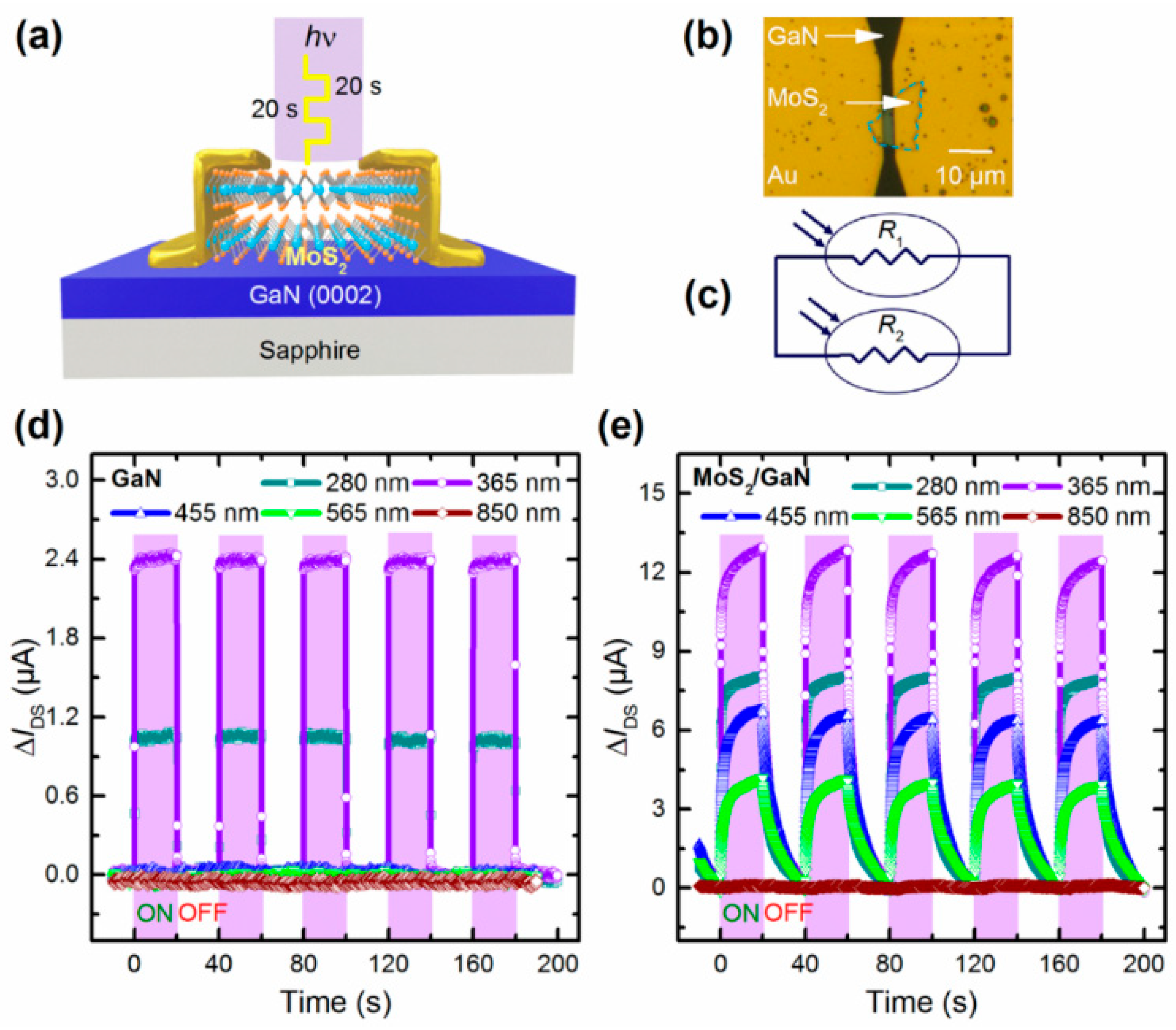
With the advent of the 5G communication era, the position of RF devices is increasingly prominent and comparable to the importance of logic devices and memory devices. Facing the problem of bandwidth growth, promoting the working frequency of RF transistors is inevitable [53]. The maximum frequency of oscillation (fmax) based on III-V materials has exceeded 1 THz [59]. To further improve the operating frequency and bandwidth, optimizing the device processes or finding materials with higher mobility such as graphene is an effective strategy. Although the RF devices made of graphene can reach the operating frequency of mainstream RF devices, the gain cannot be further improved, due to the restriction of the zero bandgap. However, MoS2 with a sizable bandgap can solve this bottleneck effectively [60].
Cheng et al. demonstrated a high-performance MoS2 RF device on a flexible substrate with an intrinsic cut-off frequency of 42 GHz and fmax up to 50 GHz, and an intrinsic gain over 30 [61]. Wu et al. reported a microwave circuit with a MoS2 self-switching diode. Ten layers of MoS2 were grown on an Al2O3/Si substrate to realize the audio spectrum of an amplitude-modulated microwave signal in the 0.9~10 GHz band [62]. Modreanu et al. fabricated RF transistors with a double-layer MoS2 channel structure, and the RF performance of the device was improved by electrostatic doping of the back gate. For MoS2 RF transistors with a 190 nm gate length, at VBG = 3 V, the external natural cutoff frequency was 6 GHz, the internal natural cutoff frequency was up to 19 GHz, and the maximum oscillation frequency was 29.7 GHz [63].
Among the flexible electronic devices, the fT and fmax of MoS2 RF transistors were higher than or comparable to those based on flexible electronic materials such as silicon film and InGaZnO [59]. Gao et al. transferred the bilayer MoS2 onto a flexible polyimide substrate to prepare high-performance RF transistors. The different gate lengths (0.3 µm, 0.6 µm, and 1 µm) affected the performance of MoS2 RF transistors. It was found that fT and fmax increased with the decrease in the gate length, and with the gate length of 0.3 µm, the external fT was 4 GHz and fMax was 10 GHz [64].
Dresselhaus et al. formed a (1T/1T’-2H) phase heterostructure of MoS2, and a Schottky diode flexible rectifier was fabricated by ohmic contact with palladium and Au electrodes, as shown in Figure 8d. Figure 8a–c show that the rectifier voltage increased with the increase in RF power, the maximum power efficiency could reach 40.1% at the 2.4 GHz band, and fT was 10 MHz. A radio-frequency energy collector was prepared by integrating with a flexible Wi-Fi antenna, as shown in Figure 8e. The radio-frequency energy collector at 2.5 cm produced an output voltage of 250 mV at 5.9 GHz. These provided a universal energy-harvesting building block, which could also be integrated with various flexible electronic systems [65].
Most MoS2-based RF transistors have been concentrated in bilayer structures because bilayer MoS2 typically has higher mobility and saturation speed than single-layer MoS2, providing a better power gain and cutoff frequency for the device. However, the high-frequency performance of MoS2 RF transistors is still lower than that of silicon transistors. Therefore, it is important to optimize the device structure or process (such as optimizing gate structure and edge contact). In addition, MoS2 with excellent mechanical properties can be used to manufacture flexible devices and, combined with RF, logic, and other fields, can achieve flexible electronic systems such as wearable devices, flexible sensors, and medical equipment.

4. Photodetectors

A photodetector is a device that converts photons into current by the photogenerated voltage effect of semiconductor materials. When a light source with strong radiation energy illuminates a semiconductor, the semiconductor material will absorb photons and generate electron–hole pairs to generate photocurrent [66]. MoS2 has a wide bandgap, layered structure, strong photoluminescence characteristics, and excellent mechanical properties. Photodetectors made of MoS2 have strong light response characteristics in the terahertz, mid-infrared, visible light, and near-infrared ranges [67]. Widely used photodetector performance indicators include responsivity, time response, specific detection rate, and spectral selectivity [68].
Zhang et al. developed a method for rapid synthesis of multilayer MoS2 films from 1 L to more than 20 L with good quality using NaCl as a promoter. Then, a monolayer-to-multilayer MoS2 photodetector was constructed, as shown in Figure 9a. Figure 9b,c illustrates the output curve of the monolayer–multilayer MoS2 heterojunction device and the outstanding rectifying ratio (103). Figure 9d depicts the band diagram of the monolayer MoS2 under high performance. In order to explore photoresponsivity, the transfer characteristic curve (Figure 9e) of the device under light and dark conditions and the light response ability under different voltages were investigated. Figure 9f shows that the device could achieve a maximum sensitivity of 104 A/W at 0 V (VGS) [69].
Wu et al. prepared a photodetector by combining MXene nanoparticles with a 2D MoS2 in a hybrid plasma structure. This strategy could improve the optical response of MoS2 and make it more sensitive to visible light. The experimental results showed that the response rate of the device was 20.67 A/W, the detectivity was 5.39 × 10¹² Jones, and the external quantum efficiency was up to 5167% [70]. Wang et al. grew a gate dielectric heap (Al2O3/HZO/TiN) on a Si substrate and transferred multilayer MoS2 to prepare an ultra-sensitive negative-capacitance MoS2 phototransistor. The HZO film could significantly enhance the optical gating effect, suppress dark current, and improve the ratio of light to dark current through a ferroelectric local electrostatic field and the ferroelectric NC effect. The experiment demonstrated that the prototype device had a high detection rate of 4.7 × 1014 cm Hz1/2W−1 and a high response rate of 96.8 AW−1 at low operating voltages of Vds = 0.5 V and Vg = 1.6 V at room temperature [71]. Walila et al. grew a 3.5 µm GaN on a sapphire substrate, and the MoS2 was mechanically stripped as the active layer. Figure 10a,b show the highly sensitive photodetector with gold and chromium as the electrode. Compared with bare GaN photodetectors, the responsivity and EQE of the photodetectors improved by 5 times, as shown in Figure 10d,e. Under the condition of 1 V bias and 365 nm excitation at 1 mW/cm2, the highest response rate and EQE were obtained, which were 1.8 × 10⁴ A/W and 6.19 × 10⁶%, respectively [24]. The GaN/MoS2 heterojunction laid a foundation for wide bandgaps and excellent photoelectric performance.
At present, the MoS2 photodetector mainly focuses on two aspects: the change in layer number and the construction of a heterojunction. The monolayer MoS2 has a low absorption surface and low quantum yield, which limits its development in photoelectric devices. In contrast, the multilayer MoS2 has a small bandgap and can improve the absorption efficiency. Especially, the MoS2-based heterojunction photodetector could achieve faster charge transfer and optical response. Optoelectronic devices require trade-offs between responsiveness and response time to meet practical needs. Although MoS2-based photodetectors have some difficulties, they still have great advantages in flexible photodetectors and integrated nano-optoelectronic systems.

5. Biosensors

Biosensors are widely used in clinical and disease treatment as a powerful tool to detect biochemical processes. The great demand for detection has promoted the development of new nanomaterials as a sensing platform [72,73]. The global spread of COVID-19 has warned people to protect their own health, and biosensors with rapid, real-time, and accurate detection can effectively contain the spread of the virus and remind people to treat themselves in a timely manner [73,74]. MoS2 attracted new interest with the multidimensional structures and structure-dependent unique electronic, electrocatalytic, and optical properties [75]. Therefore, MoS2 has been widely applied in biosensors that can detect DNA, proteins, metal ions, and other compounds [76].
Arshad et al. modified Au nanoparticles on MoS2 nanosheets to prepare bottom-gate FETs for the detection of the low-concentration C-reactive protein. The detection limit and sensitivity of BG-FETs were 8.38 fg/mL and 176 nA/g·mL−1, respectively [77]. Dai et al. prepared MoS2 on a 300 nm SiO2/Si substrate and functionalized MoS2 by combining five different DNA sequences into a DNA tetrahedron, as shown in Figure 11a. Figure 11b shows that the biosensor is extremely sensitive to the target protein (prostate-specific antigen, PSA). In phosphate-buffered brine, the detection limit was 1 fg/mL and the linear range was 1 fg/mL~100 ng/mL. Figure 11c shows that the Ids decreases as the concentration increases, and bovine serum albumin (BSA) is used as an interference signal for comparison of detection effects. Figure 11d shows that the biosensor is extremely sensitive to the target protein (prostate-specific antigen, PSA) [25].
He et al. prepared a surface plasmon resonance (SPR) biosensor with Au nanoparticles-modified MoS2 nanoflowers for IgG detection. The flower-like structure can provide more active sites for metal particles to react with target substances. The sensitivity of the MoS2-Aunps-modified sensor was 0.0472 nm/(μg/mL), which is about 3 times higher than that of an unmodified sensor (0.016 nm/(μg/mL)). The limit of detection of IgG was reduced 2.7 times (from 0.16 to 0.06 μg/mL) [78]. Kim et al. prepared MoS2 biological FETs with a nanoporous structure. Nanoporous structures could increase the edge area, using block copolymer photolithography. The surface area of the nanocycle was selectively functionalized by the newly formed suspended groups at the edge of the nanocycle. The biosensor exhibited superior detection performance in human serum and artificial saliva and resulted in a limit of detection of 1 ag/mL for cortisol [79].
This section mainly introduces the MoS2-based biosensor and the biocompatibility of the MoS2 material with biological cells, and the portability, sensitivity, and low power consumption of FETs have been widely studied and applied in biological monitoring. During the background of COVID-19, the development of wearable biosensors for rapid monitoring has become an urgent need.

6. Piezoelectric Devices

Piezoelectric properties exist in materials with centrosymmetric fractures. When strain was applied, the center of gravity of the cation and anion did not coincide, which resulted in a voltage potential at the interface between the semiconductor and the metal [80]. The mechanical flexibility and piezoelectric and photoelectric effects of MoS2 materials can meet the needs of pressure sensors, micro-electro-mechanical systems, and active flexible electronic devices [81]. A layered MoS2 material could be modified to obtain piezoelectric properties and could be applied to piezoelectric nanogenerators [82]. The piezoelectric effect can be used to collect micro-mechanical energy and convert it into electrical energy [83].
Hone et al. first reported the piezoelectric properties of monolayer MoS2 in 2014 [84]. Kim et al. prepared a monolayer MoS2 piezoelectric nanogenerator (PNG) by sulfur vacancy passivation. The output peak current and voltage of the PNG monolayer MoS2 nanoflakes treated by S increased by 3 times (100 pA) and 2 times (22 mV), respectively. In addition, the maximum power increased by nearly 10 times [85]. Hu et al. fabricated a single-layer butterfly MoS2 piezoelectric device on a polyethylene terephthalate substrate. Figure 12a,d shows the piezoelectric properties of the MoS2 single crystal (SC-MoS2) and MoS2 with grain boundaries (GB-MoS2) under external strain. Figure 12b,c shows that under the action of external stress, the current value generated by the direction of “armchair” was higher than that of the direction of “Zigzag”. Figure 12e,f shows that the GB-MoS2 current density is higher than that of SC-MoS2. It was found that the piezoelectric effect induced by the grain boundary (~ 50%) could be applied to a self-powered sensor to monitor changes in human blood pressure [26].
Xue et al. reported a new self-powered NH3 sensor, which employed monolayer MoS2 materials on PET and covered polydimethylsiloxane films, and deposited an Au electrode. The sensor could be worn on different parts of the body and was responsive with a fast response/recovery time of 18 s/16 s [86]. Willatzen et al. first calculated the piezoelectric coefficient of 3R-MoS2. Here, the 5-layer 3R-MoS2 structure had the highest piezoelectric constant in all MoS2 multilayer structures. The maximum piezoelectric constant was about 13% higher than that of the monolayer MoS2 structure [87].
The discovery of piezoelectric effects could utilize a lot of neglected energy. At present, the application of MoS2 piezoelectric properties is not mature enough. It is necessary to systematically study the piezoelectric properties, piezoelectric coefficients, and deformation direction of MoS2 with different layers to help develop high-performance piezoelectric devices. Hence, MoS2 piezoelectric sensors will realize their great potential in nanoscale electromechanical systems, micro-flexible wearable devices, and other fields in the future.

7. Synaptic Transistors

After the concept of artificial intelligence appeared, neuromorphic electronics, which simulate human brain function and information processing, have been proposed as an effective method to solve complex data processing problems [88]. The foundation of this technology is to make artificial synapses, which have low power consumption, small size, and simple structure. A MoS2 material is appropriate for the construction of artificial synapses due to its excellent electrical properties and optical response. At present, a MoS2-based artificial synapse has been applied in memory devices, programmable logic circuits, and other fields.
Roy et al. fabricated a MoS2 vertical synaptic transistor with a titanium and Au electrode. The device exhibited extremely low cycle-to-cycle variability and device-to-device variability and stability in the SET voltage and RESET power distributions. The results showed that there are 26 different conductance states in the device, and each state is maintained for at least 300 s. These devices maintained a consistent on/off ratio during the 1000 DC SET–RESET cycles [89]. Wang et al. proposed a phototransistor based on a MoS2/graphene heterostructure and an integrated triboelectric nanogenerator to simulate mechanical photon artificial synapses. Synaptic plasticity can be realized by modulating the channel conductivity of the phototransistor by regulating the mechanical displacement of a TENG. The simulation results showed that the image recognition accuracy of the artificial neural network was improved by 92% with the help of mechanical plasticizing [90].
Im et al. fabricated multilevel memory based on van der Waals heterostack (HS) N-MoSe2/N-MoS2 FETs and extended it to synaptic memory. Figure 13a shows that the synaptic stacked channel FET was used to simulate a biological synapse. Figure 13b,c illustrates that using a voltage pulse could simulate synaptic behavior. HS memory utilized the capture/de-capture phenomenon induced by VGS for programming/erasing functions. Due to the existence of a heterojunction energy barrier between MoS2 and MoS2, it could maintain a long retention time of 104 s. Based on the P-D characteristics of the device under multiple 60 s short VGS pulses, the simulated recognition rate could reach 94% on average [27], as shown in Figure 13.
The successful fabrication of artificial synapses based on MoS2 has proved the possibility of its application in non-von Neumann computing. MoS2 synaptic transistors with high performance, low power, and large-scale integration characteristics will be widely used in the brain-like chip, logic circuit, and simulated artificial neuromorphic system. However, there are still significant challenges in the fabrication technology and the structure of MoS2 synaptic transistors.

8. Conclusions

Two-dimensional MoS2 FETs have attracted wide and in-depth attention as a suitable candidate for optoelectronic devices and next-generation large-size flexible electronics. This benefited from the natural atomic layer thickness and large specific surface area of MoS2, but it can impact the influence quality, which mainly contains a contact interface and dielectric interface, and they both can then influence the performance of the MoS2 FET. Thus, in order to obtain higher-performance MoS2 FETs, it is necessary to focus on its main performance improvement strategies, including optimizing the contact behavior, regulating the conductive channel, and rationalizing the dielectric layer.
To optimize the contact behavior of MoS2 FETs, this paper reviewed metal, graphene, Mxene, and other new electrodes materials contacting with MoS2, which can adjust the Fermi level and reduce the Schottky barrier. Self-assembling monolayer functionalized electrodes are also a novel way to improve the contact barrier, which can significantly reduce the Ion/Ioff required by the device. In addition, a 2D/2D van der Waals contact is also the ideal way to optimize the contact behavior. Meanwhile, the intrinsic MoS2 is a typical N-type semiconductor, so it is difficult to prepare high-performance P-type MoS2 FETs. At the same time, the defect sites on the surface of the film will produce high resistance and hinder its electrical performance. Therefore, doping is an effective method to improve the performance of conductive channels. Metal doping and non-metal doping can improve the device mobility. More importantly, several different doping methods, such as tantalum, niobium, and He+ irradiation methods, can realize the transformation of a MoS2 FET from N-type to P-type. In addition, surface charge accumulation and leakage current due to trap charges are also key challenges for MoS2 FETs. A reasonable dielectric layer is significant to reduce leakage current and optimize stability. Although the high-K dielectric is a common solution, it can also produce trap charge. Doping dielectric layers, plasma treatment, double-K dielectric layers, etc., are proposed to improve the performance of the dielectric layer.
Functional 2D MoS2 FETs have been widely used in key and emerging fields such as logic, RF circuits, optoelectronic devices, biosensors, piezoelectric devices, and synaptic transistors. However, there are some important challenges. For example, how to obtain high-performance P-type MoS2 FETs on a large scale and build complementary circuits in logic circuits. The strong photoluminescence properties of the MoS2 material promote its application in optoelectronic devices, but its effective mechanism in photoluminescence devices and electroluminescence devices remains to be explored, and wearable high-performance biosensors are of great help to solve the current global epidemic detection. Thus, a MoS2 artificial synapse can be desired for real-time monitoring. Although its research has been very hot in recent years, there is still a long way to go in the application of a brain-like microarray and artificial neuromorphology. However, we still believe that molybdenum sulfide FETs can be used to construct novel functionalized devices and even super-large scale flexible electronic systems.
Two-dimensional MoS2 is a very suitable channel layer material for the high-performance FETs, and 2D MoS2 FETs are the promising candidate for downscaling electronics with short channels, low thickness, small volume, high speed, high sensitivity, light weight, etc. Especially, a MoS2 FET array based on a high-quality MoS2 channel will have a large degree of application in the next generation of integrated circuits and flexible electronics. However, monolayer MoS2 can better meet the high-performance requirements of short channels and even ultra-short-channel FETs. Thus, it is of great practical significance to develop the preparation process of monolayer MoS2 and MoS2 FETs performance. Thus, we believe it to be necessary to continue to extensively study in-depth fewer-layer MoS2 and MoS2-based FETs.

Author Contributions

C.W. conceived the theme and framework of the review; C.W., Y.S. and H.H. co-authored the manuscript. All authors have read and agreed to the published version of the manuscript.

Funding

This work was supported by the National Natural Science Foundation of China (No. 11604252), the Program of State Key Laboratory of Infrared Physics (No. M202001), the Program of the Key Laboratory of Artificial Microstructure, Ministry of Education (No. 13022019af002), the Science and Technology Program of Shaanxi Province (No. 2017JQ1015), and the Start-Up Funds of Xi’an Polytechnic University (No. BS15026).

Institutional Review Board Statement

Not applicable.

Informed Consent Statement

Not applicable.

Data Availability Statement

Not applicable.

Conflicts of Interest

The authors declare no conflict of interest.

References

  1. Liu, Y.; Duan, X.; Shin, H.J.; Park, S.; Huang, Y.; Duan, X. Promises and prospects of two-dimensional transistors. Nature 2021, 591, 43–53. [Google Scholar] [CrossRef] [PubMed]
  2. Jiang, B.; Yang, Z.; Liu, X.; Liu, Y.; Liao, L. Interface engineering for two-dimensional semiconductor transistors. Nano Today 2019, 25, 122–134. [Google Scholar] [CrossRef]
  3. Flores-Silva, P.A.; Borja-Hernández, C.; Magaña, C.; Acosta, D.R.; Botello-Méndez, A.R.; Serkovic-Loli, L.N. Graphene field effect transistors using TiO2 as the dielectric layer. Phys. E Low-Dimens. Syst. Nanostruct. 2020, 124, 114282. [Google Scholar] [CrossRef]
  4. Feng, X.; Huang, X.; Chen, L.; Tan, W.C.; Wang, L.; Ang, K.-W. High Mobility Anisotropic Black Phosphorus Nanoribbon Field-Effect Transistor. Adv. Funct. Mater. 2018, 28, 1801524. [Google Scholar] [CrossRef]
  5. Liu, B.; Ma, Y.; Zhang, A.; Chen, L.; Abbas, A.N.; Liu, Y.; Shen, C.; Wan, H.; Zhou, C. High-Performance WSe2 Field-Effect Transistors via Controlled Formation of In-Plane Heterojunctions. ACS Nano 2016, 10, 5153–5160. [Google Scholar] [CrossRef] [PubMed]
  6. Kumar, J.; Kuroda, M.A.; Bellus, M.Z.; Han, S.-J.; Chiu, H.-Y. Full-range electrical characteristics of WS2 transistors. Appl. Phys. Lett. 2015, 106, 123508. [Google Scholar] [CrossRef]
  7. Liu, H.; Ye, P.D. Dual-Gate MOSFET With Atomic-Layer-Deposited as Top-Gate Dielectric. IEEE Electron Device Lett. 2012, 33, 546–548. [Google Scholar] [CrossRef]
  8. Larentis, S.; Fallahazad, B.; Tutuc, E. Field-effect transistors and intrinsic mobility in ultra-thin MoSe2 layers. Appl. Phys. Lett. 2012, 101, 223104. [Google Scholar] [CrossRef]
  9. Liu, Y.; Zhao, S.; Luo, L.; Wang, J.; Zhu, Z.; Xiang, Q.; Deng, Y.; Zhao, Z. Mesenchymal stem cell-derived exosomes ameliorate erection by reducing oxidative stress damage of corpus cavernosum in a rat model of artery injury. J. Cell Mol. Med. 2019, 23, 7462–7473. [Google Scholar] [CrossRef]
  10. Huang, Y.; Pan, Y.H.; Yang, R.; Bao, L.H.; Meng, L.; Luo, H.L.; Cai, Y.Q.; Liu, G.D.; Zhao, W.J.; Zhou, Z.; et al. Universal mechanical exfoliation of large-area 2D crystals. Nat. Commun. 2020, 11, 2453. [Google Scholar] [CrossRef]
  11. Xu, X.; Zhang, C.; Hota, M.K.; Liu, Z.; Zhang, X.; Alshareef, H.N. Enhanced Quality of Wafer-Scale MoS2 Films by a Capping Layer Annealing Process. Adv. Funct. Mater. 2020, 30, 1908040. [Google Scholar] [CrossRef]
  12. Chang, M.C.; Ho, P.H.; Tseng, M.F.; Lin, F.Y.; Hou, C.H.; Lin, I.K.; Wang, H.; Huang, P.P.; Chiang, C.H.; Yang, Y.C.; et al. Fast growth of large-grain and continuous MoS2 films through a self-capping vapor-liquid-solid method. Nat. Commun. 2020, 11, 3682. [Google Scholar] [CrossRef] [PubMed]
  13. Xu, X.; Wang, Z.; Lopatin, S.; Quevedo-Lopez, M.A.; Alshareef, H.N. Wafer scale quasi single crystalline MoS2 realized by epitaxial phase conversion. 2D Mater. 2018, 6, 015030. [Google Scholar] [CrossRef]
  14. Han, B.; Zhao, Y.; Ma, C.; Wang, C.; Tian, X.; Wang, Y.; Hu, W.; Samori, P. Asymmetric Chemical Functionalization of Top-Contact Electrodes: Tuning the Charge Injection for High-Performance MoS2 Field-Effect Transistors and Schottky Diodes. Adv. Mater. 2022, 34, e2109445. [Google Scholar] [CrossRef] [PubMed]
  15. Seo, D.; Lee, D.Y.; Kwon, J.; Lee, J.J.; Taniguchi, T.; Watanabe, K.; Lee, G.-H.; Kim, K.S.; Hone, J.; Kim, Y.D.; et al. High-performance monolayer MoS2 field-effect transistor with large-scale nitrogen-doped graphene electrodes for Ohmic contact. Appl. Phys. Lett. 2019, 115, 012104. [Google Scholar] [CrossRef]
  16. Li, H.; Cheng, M.; Wang, P.; Du, R.; Song, L.; He, J.; Shi, J. Reducing Contact Resistance and Boosting Device Performance of Monolayer MoS2 by In Situ Fe Doping. Adv. Mater. 2022, 34, e2200885. [Google Scholar] [CrossRef]
  17. Zhang, Z.; Su, M.; Li, G.; Wang, J.; Zhang, X.; Ho, J.C.; Wang, C.; Wan, D.; Liu, X.; Liao, L. Stable Hysteresis-Free MoS2 Transistors With Low-k/High-k Bilayer Gate Dielectrics. IEEE Electron Device Lett. 2020, 41, 1036–1039. [Google Scholar] [CrossRef]
  18. Liu, Y.; Gu, F. A wafer-scale synthesis of monolayer MoS2 and their field-effect transistors toward practical applications. Nanoscale Adv. 2021, 3, 2117–2138. [Google Scholar] [CrossRef]
  19. Yang, P.; Zou, X.; Zhang, Z.; Hong, M.; Shi, J.; Chen, S.; Shu, J.; Zhao, L.; Jiang, S.; Zhou, X.; et al. Batch production of 6-inch uniform monolayer molybdenum disulfide catalyzed by sodium in glass. Nat. Commun. 2018, 9, 979. [Google Scholar] [CrossRef]
  20. Liu, F.; Wu, W.; Bai, Y.; Chae, S.H.; Li, Q.; Wang, J.; Hone, J.; Zhu, X.-Y. Disassembling 2D van der Waals crystals into macroscopic monolayers and reassembling into artificial lattices. Science 2020, 367, 903–906. [Google Scholar] [CrossRef]
  21. Shen, P.C.; Su, C.; Lin, Y.; Chou, A.S.; Cheng, C.C.; Park, J.H.; Chiu, M.H.; Lu, A.Y.; Tang, H.L.; Tavakoli, M.M.; et al. Ultralow contact resistance between semimetal and monolayer semiconductors. Nature 2021, 593, 211–217. [Google Scholar] [CrossRef] [PubMed]
  22. Kim, J.Y.; Park, H.J.; Lee, S.H.; Seo, C.; Kim, J.; Joo, J. Distinctive Field-Effect Transistors and Ternary Inverters Using Cross-Type WSe2/MoS2 Heterojunctions Treated with Polymer Acid. ACS Appl. Mater. Interfaces 2020, 12, 36530–36539. [Google Scholar] [CrossRef] [PubMed]
  23. Krasnozhon, D.; Lembke, D.; Nyffeler, C.; Leblebici, Y.; Kis, A. MoS2 transistors operating at gigahertz frequencies. Nano Lett. 2014, 14, 5905–5911. [Google Scholar] [CrossRef] [PubMed]
  24. Jain, S.K.; Low, M.X.; Taylor, P.D.; Tawfik, S.A.; Spencer, M.J.S.; Kuriakose, S.; Arash, A.; Xu, C.; Sriram, S.; Gupta, G.; et al. 2D/3D Hybrid of MoS2/GaN for a High-Performance Broadband Photodetector. ACS Appl. Electron. Mater. 2021, 3, 2407–2414. [Google Scholar] [CrossRef]
  25. Zhang, Y.; Feng, D.; Xu, Y.; Yin, Z.; Dou, W.; Habiba, U.E.; Pan, C.; Zhang, Z.; Mou, H.; Deng, H.; et al. DNA-based functionalization of two-dimensional MoS2 FET biosensor for ultrasensitive detection of PSA. Appl. Surf. Sci. 2021, 548, 149169. [Google Scholar] [CrossRef]
  26. Dai, M.; Zheng, W.; Zhang, X.; Wang, S.; Lin, J.; Li, K.; Hu, Y.; Sun, E.; Zhang, J.; Qiu, Y.; et al. Enhanced Piezoelectric Effect Derived from Grain Boundary in MoS2 Monolayers. Nano Lett. 2020, 20, 201–207. [Google Scholar] [CrossRef]
  27. Jeong, Y.; Lee, H.J.; Park, J.; Lee, S.; Jin, H.-J.; Park, S.; Cho, H.; Hong, S.; Kim, T.; Kim, K.; et al. Engineering MoSe2/MoS2 heterojunction traps in 2D transistors for multilevel memory, multiscale display, and synaptic functions. npj 2D Mater. Appl. 2022, 6, 23. [Google Scholar] [CrossRef]
  28. Ma, X.; Dai, Y.; Yu, L.; Huang, B. Interface Schottky barrier engineering via strain in metal-semiconductor composites. Nanoscale 2016, 8, 1352–1359. [Google Scholar] [CrossRef]
  29. Zhong, H.; Quhe, R.; Wang, Y.; Ni, Z.; Ye, M.; Song, Z.; Pan, Y.; Yang, J.; Yang, L.; Lei, M.; et al. Interfacial Properties of Monolayer and Bilayer MoS2 Contacts with Metals: Beyond the Energy Band Calculations. Sci. Rep. 2016, 6, 21786. [Google Scholar] [CrossRef]
  30. Zhao, P.; Jin, H.; Lv, X.; Huang, B.; Ma, Y.; Dai, Y. Modified MXene: Promising electrode materials for constructing Ohmic contacts with MoS2 for electronic device applications. Phys. Chem. Chem. Phys. 2018, 20, 16551–16557. [Google Scholar] [CrossRef]
  31. Lee, I.; Kim, J.N.; Kang, W.T.; Shin, Y.S.; Lee, B.H.; Yu, W.J. Schottky Barrier Variable Graphene/Multilayer-MoS2 Heterojunction Transistor Used to Overcome Short Channel Effects. ACS Appl. Mater. Interfaces 2020, 12, 2854–2861. [Google Scholar] [CrossRef] [PubMed]
  32. Zhang, C. Interfacial assembly of two-dimensional MXenes. J. Energy Chem. 2021, 60, 417–434. [Google Scholar] [CrossRef]
  33. Armin Vahidmohammadi, J.R.Y.G. The world of two-dimensional carbides and nitrides (MXenes). Science 2021, e372, abf1581. [Google Scholar] [CrossRef]
  34. Zhou, Y.; Zhuge, X.; An, P.; Du, S. First-principles investigations on MXene-blue phosphorene and MXene-MoS2 transistors. Nanotechnology 2020, 31, 395203. [Google Scholar] [CrossRef] [PubMed]
  35. Kim, C.; Lee, K.Y.; Moon, I.; Issarapanacheewin, S.; Yoo, W.J. Metallic contact induced van der Waals gap in a MoS2 FET. Nanoscale 2019, 11, 18246–18254. [Google Scholar] [CrossRef]
  36. Manish Chhowalla, D.J.; Zhang, H. Two-dimensional semiconductors for transistors. Nat. Rev. Mater. 2016, 1, 16052. [Google Scholar] [CrossRef]
  37. Kim, E.; Lee, Y.; Ko, C.; Park, Y.; Yeo, J.; Chen, Y.; Choe, H.S.; Allen, F.I.; Rho, J.; Tongay, S.; et al. Tuning the optical and electrical properties of MoS2 by selective Ag photo-reduction. Appl. Phys. Lett. 2018, 113, 013105. [Google Scholar] [CrossRef]
  38. Wei, Z.; Tang, J.; Li, X.; Chi, Z.; Wang, Y.; Wang, Q.; Han, B.; Li, N.; Huang, B.; Li, J.; et al. Wafer-Scale Oxygen-Doped MoS2 Monolayer. Small Methods 2021, 5, e2100091. [Google Scholar] [CrossRef]
  39. Li, M.; Wu, X.; Guo, W.; Liu, Y.; Xiao, C.; Ou, T.; Zheng, Y.; Wang, Y. Controllable p-type doping of monolayer MoS2 with tantalum by one-step chemical vapor deposition. J. Mater. Chem. C 2022, 10, 7662–7673. [Google Scholar] [CrossRef]
  40. Ma, Z.; Zhang, L.; Zhou, C.; Chan, M. High Current Nb-Doped P-Channel MoS₂ Field-Effect Transistor Using Pt Contact. IEEE Electron Device Lett. 2021, 42, 343–346. [Google Scholar] [CrossRef]
  41. Han, S.W.; Yun, W.S.; Kim, H.; Kim, Y.; Kim, D.H.; Ahn, C.W.; Ryu, S. Hole doping effect of MoS2 via electron capture of He(+) ion irradiation. Sci. Rep. 2021, 11, 23590. [Google Scholar] [CrossRef]
  42. Park, W.; Pak, Y.; Jang, H.Y.; Nam, J.H.; Kim, T.H.; Oh, S.; Choi, S.M.; Kim, Y.; Cho, B. Improvement of the Bias Stress Stability in 2D MoS2 and WS2 Transistors with a TiO2 Interfacial Layer. Nanomaterials 2019, 9, 1155. [Google Scholar] [CrossRef] [PubMed]
  43. Siao, M.D.; Shen, W.C.; Chen, R.S.; Chang, Z.W.; Shih, M.C.; Chiu, Y.P.; Cheng, C.M. Two-dimensional electronic transport and surface electron accumulation in MoS2. Nat. Commun. 2018, 9, 1442. [Google Scholar] [CrossRef] [PubMed]
  44. Jeong, Y.; Jin, H.J.; Park, J.H.; Cho, Y.; Kim, M.; Hong, S.; Jo, W.; Yi, Y.; Im, S. Low Voltage and Ferroelectric 2D Electron Devices Using Lead-Free BaxSr1-xTiO3 and MoS2 Channel. Adv. Funct. Mater. 2019, 30, 1908210. [Google Scholar] [CrossRef]
  45. Kolla, L.G.; Bhattacharjee, S.; S, M.; Bhat, N. High Performance HfO2 Back Gated Multilayer MoS2 transistors. IEEE Electron Device Lett. 2016, 37, 1. [Google Scholar] [CrossRef]
  46. Yu, Z.; Ong, Z.-Y.; Li, S.; Xu, J.-B.; Zhang, G.; Zhang, Y.-W.; Shi, Y.; Wang, X. Analyzing the Carrier Mobility in Transition-Metal Dichalcogenide MoS2Field-Effect Transistors. Adv. Funct. Mater. 2017, 27, 1604093. [Google Scholar] [CrossRef]
  47. Ma, N.; Jena, D. Charge Scattering and Mobility in Atomically Thin Semiconductors. Phys. Rev. X 2014, 4, 011043. [Google Scholar] [CrossRef]
  48. Yu, Z.; Ong, Z.Y.; Pan, Y.; Cui, Y.; Xin, R.; Shi, Y.; Wang, B.; Wu, Y.; Chen, T.; Zhang, Y.W.; et al. Realization of Room-Temperature Phonon-Limited Carrier Transport in Monolayer MoS2 by Dielectric and Carrier Screening. Adv. Mater. 2016, 28, 547–552. [Google Scholar] [CrossRef] [PubMed]
  49. Song, X.; Xu, J.; Liu, L.; Lai, P.-T. Comprehensive investigation on CF4/O2-plasma treating the interfaces of stacked gate dielectric in MoS2 transistors. Appl. Surf. Sci. 2021, 542, 148437. [Google Scholar] [CrossRef]
  50. Song, X.; Xu, J.; Liu, L.; Deng, Y.; Lai, P.T.; Tang, W.M. Optimizing Al-doped ZrO2 as the gate dielectric for MoS2 field-effect transistors. Nanotechnology 2020, 31, 135206. [Google Scholar] [CrossRef]
  51. Zhao, X.-Y.; Xu, J.-P.; Liu, L.; Li, Z. Improved Electrical Properties of Top-Gate MoS2 Transistor With NH3-Plasma Treated HfO2 as Gate Dielectric. IEEE Electron Device Lett. 2020, 41, 1364–1367. [Google Scholar] [CrossRef]
  52. Li, W.; Zhou, J.; Cai, S.; Yu, Z.; Zhang, J.; Fang, N.; Li, T.; Wu, Y.; Chen, T.; Xie, X.; et al. Uniform and ultrathin high-κ gate dielectrics for two-dimensional electronic devices. Nat. Electron. 2019, 2, 563–571. [Google Scholar] [CrossRef]
  53. Zeng, S.; Tang, Z.; Liu, C.; Zhou, P. Electronics based on two-dimensional materials: Status and outlook. Nano Res. 2020, 14, 1752–1767. [Google Scholar] [CrossRef]
  54. Liu, L.; Lu, Y.; Guo, J. On Monolayer MoS2 Field-Effect Transistors at the Scaling Limit. IEEE Trans. Electron Devices 2013, 60, 4133–4139. [Google Scholar] [CrossRef]
  55. Wang, H.; Yu, L.; Lee, Y.H.; Shi, Y.; Hsu, A.; Chin, M.L.; Li, L.J.; Dubey, M.; Kong, J.; Palacios, T. Integrated circuits based on bilayer MoS(2) transistors. Nano Lett. 2012, 12, 4674–4680. [Google Scholar] [CrossRef] [PubMed]
  56. Wang, L.; Chen, L.; Wong, S.L.; Huang, X.; Liao, W.; Zhu, C.; Lim, Y.F.; Li, D.; Liu, X.; Chi, D.; et al. Electronic Devices and Circuits Based on Wafer-Scale Polycrystalline Monolayer MoS2 by Chemical Vapor Deposition. Adv. Electron. Mater. 2019, 5, 1900393. [Google Scholar] [CrossRef]
  57. Yi, J.; Sun, X.; Zhu, C.; Li, S.; Liu, Y.; Zhu, X.; You, W.; Liang, D.; Shuai, Q.; Wu, Y.; et al. Double-Gate MoS2 Field-Effect Transistors with Full-Range Tunable Threshold Voltage for Multifunctional Logic Circuits. Adv. Mater. 2021, 33, e2101036. [Google Scholar] [CrossRef]
  58. Liu, C.; Chen, H.; Hou, X.; Zhang, H.; Han, J.; Jiang, Y.G.; Zeng, X.; Zhang, D.W.; Zhou, P. Small footprint transistor architecture for photoswitching logic and in situ memory. Nat. Nanotechnol. 2019, 14, 662–667. [Google Scholar] [CrossRef]
  59. Lai, R.; Mei, X.B.; Deal, W.R.; Yoshida, W.; Kim, Y.M.; Liu, P.H.; Lee, J.; Uyeda, J.; Radisic, V.; Lange, M.; et al. Sub 50 nm InP HEMT Device with Fmax Greater than 1 THz. In Proceedings of the 2007 IEEE International Electron Devices Meeting, Washington, DC, USA, 10–12 December 2007; pp. 609–611. [Google Scholar]
  60. Zhu, W.; Low, T.; Wang, H.; Ye, P.; Duan, X. Nanoscale electronic devices based on transition metal dichalcogenides. 2D Mater. 2019, 6, 032004. [Google Scholar] [CrossRef]
  61. Cheng, R.; Jiang, S.; Chen, Y.; Liu, Y.; Weiss, N.; Cheng, H.C.; Wu, H.; Huang, Y.; Duan, X. Few-layer molybdenum disulfide transistors and circuits for high-speed flexible electronics. Nat. Commun. 2014, 5, 5143. [Google Scholar] [CrossRef]
  62. Gao, Q.; Zhang, Z.; Xu, X.; Song, J.; Li, X.; Wu, Y. Scalable high performance radio frequency electronics based on large domain bilayer MoS2. Nat. Commun. 2018, 9, 4778. [Google Scholar] [CrossRef] [PubMed]
  63. Dragoman, M.; Aldrigo, M.; Connolly, J.; Povey, I.M.; Iordanescu, S.; Dinescu, A.; Vasilache, D.; Modreanu, M. MoS2 radio: Detecting radio waves with a two-dimensional transition metal dichalcogenide semiconductor. Nanotechnology 2020, 31, 06LT01. [Google Scholar] [CrossRef] [PubMed]
  64. Gao, Q.; Zhang, C.; Yang, K.; Pan, X.; Zhang, Z.; Yang, J.; Yi, Z.; Chi, F.; Liu, L. High-Performance CVD Bilayer MoS2 Radio Frequency Transistors and Gigahertz Mixers for Flexible Nanoelectronics. Micromachines 2021, 12, 451. [Google Scholar] [CrossRef]
  65. Zhang, X.; Grajal, J.; Vazquez-Roy, J.L.; Radhakrishna, U.; Wang, X.; Chern, W.; Zhou, L.; Lin, Y.; Shen, P.C.; Ji, X.; et al. Two-dimensional MoS2-enabled flexible rectenna for Wi-Fi-band wireless energy harvesting. Nature 2019, 566, 368–372. [Google Scholar] [CrossRef] [PubMed]
  66. Ye, M.; Zhang, D.; Yap, Y. Recent Advances in Electronic and Optoelectronic Devices Based on Two-Dimensional Transition Metal Dichalcogenides. Electronics 2017, 6, 43. [Google Scholar] [CrossRef]
  67. Long, M.; Wang, P.; Fang, H.; Hu, W. Progress, Challenges, and Opportunities for 2D Material Based Photodetectors. Adv. Funct. Mater. 2018, 29, 1803807. [Google Scholar] [CrossRef]
  68. Cheng, J.; Wang, C.; Zou, X.; Liao, L. Recent Advances in Optoelectronic Devices Based on 2D Materials and Their Heterostructures. Adv. Opt. Mater. 2019, 7, 1800441. [Google Scholar] [CrossRef]
  69. Yang, P.; Zhang, Z.; Sun, M.; Lin, F.; Cheng, T.; Shi, J.; Xie, C.; Shi, Y.; Jiang, S.; Huan, Y.; et al. Thickness Tunable Wedding-Cake-like MoS2 Flakes for High-Performance Optoelectronics. ACS Nano 2019, 13, 3649–3658. [Google Scholar] [CrossRef]
  70. Zou, J.; Huang, Y.; Wang, W.; Li, C.; Wei, S.; Liu, H.; Luo, L.; Du, W.; Shen, K.; Ren, A.; et al. Plasmonic MXene Nanoparticle-Enabled High-Performance Two-Dimensional MoS2 Photodetectors. ACS Appl. Mater. Interfaces 2022, 14, 8243–8250. [Google Scholar] [CrossRef]
  71. Tu, L.; Cao, R.; Wang, X.; Chen, Y.; Wu, S.; Wang, F.; Wang, Z.; Shen, H.; Lin, T.; Zhou, P.; et al. Ultrasensitive negative capacitance phototransistors. Nat. Commun. 2020, 11, 101. [Google Scholar] [CrossRef] [Green Version]
  72. Hu, Y.; Huang, Y.; Tan, C.; Zhang, X.; Lu, Q.; Sindoro, M.; Huang, X.; Huang, W.; Wang, L.; Zhang, H. Two-dimensional transition metal dichalcogenide nanomaterials for biosensing applications. Mater. Chem. Front. 2017, 1, 24–36. [Google Scholar] [CrossRef]
  73. Fathi-Hafshejani, P.; Azam, N.; Wang, L.; Kuroda, M.A.; Hamilton, M.C.; Hasim, S.; Mahjouri-Samani, M. Two-Dimensional-Material-Based Field-Effect Transistor Biosensor for Detecting COVID-19 Virus (SARS-CoV-2). ACS Nano 2021, 15, 11461–11469. [Google Scholar] [CrossRef]
  74. Mojsoska, B.; Larsen, S.; Olsen, D.A.; Madsen, J.S.; Brandslund, I.; Alatraktchi, F.A. Rapid SARS-CoV-2 Detection Using Electrochemical Immunosensor. Sensors 2021, 21, 390. [Google Scholar] [CrossRef]
  75. Barua, S.; Dutta, H.S.; Gogoi, S.; Devi, R.; Khan, R. Nanostructured MoS2-Based Advanced Biosensors: A Review. ACS Appl. Nano Mater. 2017, 1, 2–25. [Google Scholar] [CrossRef]
  76. Yan, L.; Shi, H.; Sui, X.; Deng, Z.; Gao, L. MoS2-DNA and MoS2 based sensors. RSC Adv. 2017, 7, 23573–23582. [Google Scholar] [CrossRef]
  77. Dalila, N.R.; Arshad, M.K.M.; Gopinath, S.C.B.; Nuzaihan, M.N.M.; Fathil, M.F.M. Molybdenum disulfide-gold nanoparticle nanocomposite in field-effect transistor back-gate for enhanced C-reactive protein detection. Mikrochim. Acta 2020, 187, 588. [Google Scholar] [CrossRef] [PubMed]
  78. Zhao, P.; Chen, Y.; Chen, Y.; Hu, S.; Chen, H.; Xiao, W.; Liu, G.; Tang, Y.; Shi, J.; He, Z.; et al. A MoS2 nanoflower and gold nanoparticle-modified surface plasmon resonance biosensor for a sensitivity-improved immunoassay. J. Mater. Chem. C 2020, 8, 6861–6868. [Google Scholar] [CrossRef]
  79. Park, H.; Baek, S.; Sen, A.; Jung, B.; Shim, J.; Park, Y.C.; Lee, L.P.; Kim, Y.J.; Kim, S. Ultrasensitive and Selective Field-Effect Transistor-Based Biosensor Created by Rings of MoS2 Nanopores. ACS Nano 2022, 16, 1826–1835. [Google Scholar] [CrossRef]
  80. Zhang, Q.; Zuo, S.; Chen, P.; Pan, C. Piezotronics in two-dimensional materials. InfoMat 2021, 3, 987–1007. [Google Scholar] [CrossRef]
  81. Peng, Y.; Que, M.; Tao, J.; Wang, X.; Lu, J.; Hu, G.; Wan, B.; Xu, Q.; Pan, C. Progress in piezotronic and piezo-phototronic effect of 2D materials. 2D Mater. 2018, 5, 042003. [Google Scholar] [CrossRef] [Green Version]
  82. Hinchet, R.; Khan, U.; Falconi, C.; Kim, S.-W. Piezoelectric properties in two-dimensional materials: Simulations and experiments. Mater. Today 2018, 21, 611–630. [Google Scholar] [CrossRef]
  83. Wu, T.; Song, Y.; Shi, Z.; Liu, D.; Chen, S.; Xiong, C.; Yang, Q. High-performance nanogenerators based on flexible cellulose nanofibril/MoS2 nanosheet composite piezoelectric films for energy harvesting. Nano Energy 2021, 80, 105541. [Google Scholar] [CrossRef]
  84. Wu, W.; Wang, L.; Li, Y.; Zhang, F.; Lin, L.; Niu, S.; Chenet, D.; Zhang, X.; Hao, Y.; Heinz, T.F.; et al. Piezoelectricity of single-atomic-layer MoS2 for energy conversion and piezotronics. Nature 2014, 514, 470–474. [Google Scholar] [CrossRef] [PubMed]
  85. Han, S.A.; Kim, T.H.; Kim, S.K.; Lee, K.H.; Park, H.J.; Lee, J.H.; Kim, S.W. Point-Defect-Passivated MoS2 Nanosheet-Based High Performance Piezoelectric Nanogenerator. Adv. Mater. 2018, 30, e1800342. [Google Scholar] [CrossRef]
  86. Zhang, D.; Yang, Z.; Li, P.; Pang, M.; Xue, Q. Flexible self-powered high-performance ammonia sensor based on Au-decorated MoSe2 nanoflowers driven by single layer MoS2-flake piezoelectric nanogenerator. Nano Energy 2019, 65, 103974. [Google Scholar] [CrossRef]
  87. Dan, T.; Willatzen, M.; Wang, Z.L. Prediction of strong piezoelectricity in 3R-MoS2 multilayer structures. Nano Energy 2019, 56, 512–515. [Google Scholar] [CrossRef]
  88. Zhu, Y.; He, Y.; Jiang, S.; Zhu, L.; Chen, C.; Wan, Q. Indium–gallium–zinc–oxide thin-film transistors: Materials, devices, and applications. J. Semicond. 2021, 42, 031101. [Google Scholar] [CrossRef]
  89. Krishnaparsad, A.D.; Han, S.S.; Shen, Y.Q.; Chung, H.S.; Bae, T.S.; Yoo, C.; Jung, Y.; Lanza, M.; Roy, T. MoS2 Synapses with Ultra-low Variability and Their Implementation in Boolean Logic. ACS Nano 2022, 16, 2866–2876. [Google Scholar] [CrossRef]
  90. Yu, J.; Yang, X.; Gao, G.; Xiong, Y.; Wang, Y.; Han, J.; Chen, Y.; Zhang, H.; Sun, Q.; Wang, Z.L. Bioinspired mechano-photonic artificial synapse based on graphene/MoS2 heterostructure. Sci. Adv. 2021, 7, eabd9117. [Google Scholar] [CrossRef]
Figure 1. MoS2 FET performance improvement strategies and applications. (a) Schematic of monolayer MoS2 FET (reprinted/adapted with permission from Ref. [21]. Copyright 2021 Springer Nature). (b) Improving MoS2 FET performance by optimizing contact behavior (reprinted/adapted with permission from Ref. [14]. Copyright 2022 Wiley). (c) Improving MoS2 FET performance by regulating conductive channel (reprinted/adapted with permission from Ref. [16]. Copyright 2022 Wiley). (d) Improving MoS2 FET performance by rationalizing dielectric layer (reprinted/adapted with permission from Ref. [17]. Copyright 2020 IEEE). The applications of MoS2 FET in (e) logic circuits (reprinted/adapted with permission from Ref. [22]. Copyright 2020 American Chemical Society); (f) radio-frequency circuits (reprinted/adapted with permission from Ref. [23]. Copyright 2014 American Chemical Society); (g) optoelectronic devices (reprinted/adapted with permission from Ref. [24]. Copyright 2021 American Chemical Society); (h) biosensors (reprinted/adapted with permission from Ref. [25]. Copyright 2021 Elsevier); (i) piezoelectric devices (reprinted/adapted with permission from Ref. [26]. Copyright 2020 American Chemical Society); (j) synaptic transistors (reprinted/adapted with permission from Ref. [27]. Copyright 2022 American Chemical Society).
Nanomaterials 12 03233 g001
Figure 2. (a) Structure diagram of asymmetric MoS2 FETs. (b) Semilogarithmic plot of the Ids-Vds. (c) Rectification ratio. (df) Energy band diagram at thermodynamic equilibrium, positively biased source–drain, and negatively biased source–drain, respectively. (Reprinted/adapted with permission from Ref. [14]. Copyright 2022 Wiley).
Nanomaterials 12 03233 g002
Figure 3. Electrical characteristics of MoS2/pristine Gr contact device: (a) Transfer characteristic (left axis) and semilogarithm (right axis). (b) Output characteristic. (c) Schematic diagram of band alignment. Electrical characteristics of MoS2/NGr contact device: (d) Transfer characteristic (left axis) and semilogarithm (right axis). (e) Output characteristic. (f) Schematic diagram of band alignment. (Reprinted/adapted with permission from Ref. [15]. Copyright 2019 American Institute of Physics).
Nanomaterials 12 03233 g003
Figure 4. (a) Schematic diagram and OM graph of monolayer Fe-MoS2 device. (b) Transfer characteristic of MoS2-based devices. (c) Temperature vs. transfer characteristic. The inset shows the MIT area. (d) Electron mobility vs. temperature. (e) Arrhenius plots. (f) Energy barriers and energy band of the monolayer Fe-MoS2. (Reprinted/adapted with permission from Ref. [16]. Copyright 2022 Wiley).
Nanomaterials 12 03233 g004
Figure 5. (a) Schematic diagram of the conversion of n-type MoS2. The negative binding energy shifts of Mo 3d, S 2p, and valence band photoemission spectra depend on (b) the ion energy band, and (c) irradiation time of He+ ion irradiation. (Reprinted/adapted with permission from Ref. [41]. Copyright 2022 Springer Nature).
Nanomaterials 12 03233 g005
Figure 6. (a) Structure diagram of MoS2 transistor. (b) The OM graph of MoS2 transistor. (c) Ferroelectric characteristics of the different dielectrics. (df) Transfer properties of the MoS2 transistors with different gate dielectrics, at VD = 1 V (Red), 0.5 V (black), and 0.1 V (blue), receptively. The insets are the enlarged figure of the transfer curve with VD = 1 V. (Reprinted/adapted with permission from Ref. [17]. Copyright 2020 IEEE).
Nanomaterials 12 03233 g006
Figure 7. (a) Schematic diagram of ternary inverter by cross-type p–n heterojunction WSe2/MoS2-based FETs. (b) Logic circuit for ternary inverter. (c) Vout vs. Vin characteristic curves. (d) Characteristics of ternary inverter (red markers). Transfer characteristic curves of device (blue markers) and WSe2-based FETs (green markers). (Reprinted/adapted with permission from Ref. [22]. Copyright 2020 American Chemical Society).
Nanomaterials 12 03233 g007
Figure 8. MoS2 phase-junction rectenna as a wireless RF energy harvester: (a) Output voltage vs. input RF power. (b) Power efficiency of MoS2 rectifiers vs. input power. (c) Output voltage vs. frequency. (d) Flexible MoS2 wireless energy harvesting. The illustrative I–t curves correspond to the a.c. (blue arrow) and d.c. (red arrow) currents. (e) MoS2 rectenna on Kapton. (Reprinted/adapted with permission from Ref. [65]. Copyright 2019 Springer Nature).
Nanomaterials 12 03233 g008
Figure 9. (a) Schematic of the monolayer−multilayer (1L–25L) MoS2 heterojunction device. (b) Ids-Vds characteristics. (c) Rectification ratio as Vgs. (d) Band diagram of the 1 L-ML MoS2 heterojunction in the off state (Vgs = 0; Vds = 0). (e) Ids-Vgs characteristics. The inset is the OM graph of the device. (f) Vgs vs. photoresponsivity. (Reprinted/adapted with permission from Ref. [69]. Copyright 2019 American Chemical Society).
Nanomaterials 12 03233 g009
Figure 10. (a) Device structure of MoS2/GaN photodetector. (b) OM graph of the hybrid device. (c) Equivalent circuit diagram of the hybrid device. Photoresponse measurements of (d) GaN devices and (e) MoS2/GaN devices. (Reprinted/adapted with permission from Ref. [24]. Copyright 2021 American Chemical Society).
Nanomaterials 12 03233 g010
Figure 11. (a) Schematic diagram of 3D MoS2 biosensor. (b) Real-time detection (Vds= 0.5 V) of different concentrations. (c) Response time curve. (d) Response variation vs. PSA concentrations. (Reprinted/adapted with permission from Ref. [25]. Copyright 2021 Elsevier).
Nanomaterials 12 03233 g011
Figure 12. Schematic of a piezoelectric device based on (a) single-crystal MoS2 flake and (d) grain boundaries of MoS2 flake. Recorded current outputs of the SC-MoS2 devices are (b) zigzag and (c) armchair, and that of the (e) GB-MoS2 piezoelectric device is perpendicular. (f) Statistical data for the current density of different monolayer MoS2-based piezoelectric devices (reprinted/adapted with permission from Ref. [26]. Copyright 2020 American Chemical Society).
Nanomaterials 12 03233 g012
Figure 13. Synaptic memory behavior of stack channel FETs. (a) Schematic of a biological synapse in neuron system and synaptic stack channel FETs for neuromorphic function. (b) Illustration of a VPre pulse train. (c) Monitored P-D plots vs. the diverse amplitude. (d) Two P-D conductance plots with GMax/GMin values. (e) Schematics of multilayer perceptron neural network for classification of MNIST handwritten digits. (f) Circuit diagram of artificial neural network. (g) Simulation results vs. actual P-D behavior. (Reprinted/adapted with permission from Ref. [27]. Copyright 2022 American Chemical Society).
Nanomaterials 12 03233 g013
Table 1. Overview summary comparison of emerging 2D materials-based FETs.
MaterialsTechnologyConfigurationContact ElectrodeDielectricMobility (cm2/Vs)Ion/IoffSS (mV/dec)Ref.
MoS2 ExfoliationDual-gatedNi/AuAl2O3517108140[7]
CVDBack-gatedTi/AuHfO2118108/[9]
Au-assisted ExfoliationBack-gatedTi/AuSiO225107100[10]
MOCVDTop-gatedAu/TiSiO222105/[11]
VLSBack-gatedAuSiO233108980[12]
PLDTop-gatedAu/TiHfO29105/[13]
ExfoliationTop-gatedAuSiO2/Cytop31107/[14]
ExfoliationBack-gatedGrapheneSiO29106/[15]
APCVDBack-gatedCr/AuSiO254108/[16]
ExfoliationTop-gatedCr/AuPMMA/P(VDF-TrFE)/107/[17]
WSe2 CVDBack-gatedTi/PdBN9210/[5]
MoSe2ExfoliationBack-gatedNiSiO250106/[8]
WS2 ExfoliationBack-gatedTi/AuSiO22010670[6]
BPExfoliationTop-gatedNi/AuSiO2862102563[4]
GrapheneCVDBack-gatedCr/AuTiO21872/[3]
Publisher’s Note: MDPI stays neutral with regard to jurisdictional claims in published maps and institutional affiliations.

