
Efficient Nanocrystal Photovoltaics with PTAA as Hole Transport Layer

Abstract
:1. Introduction
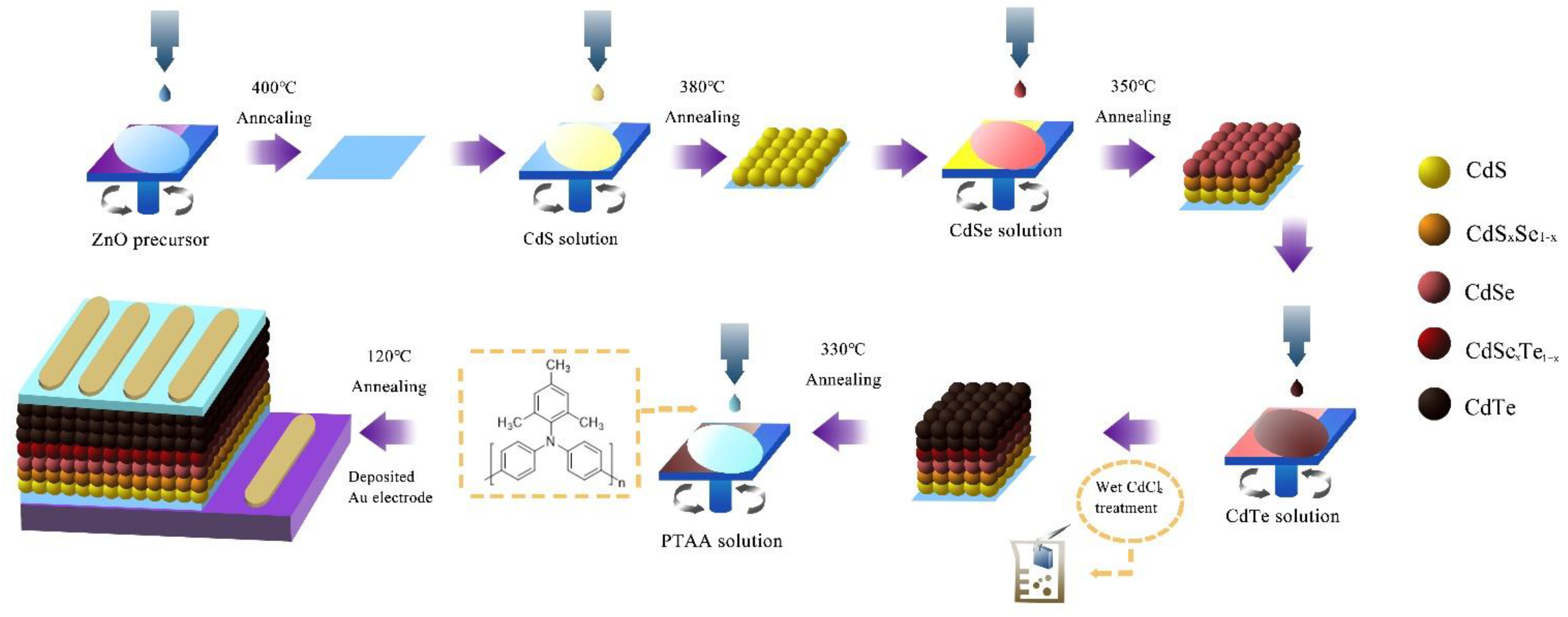
2. Experiment
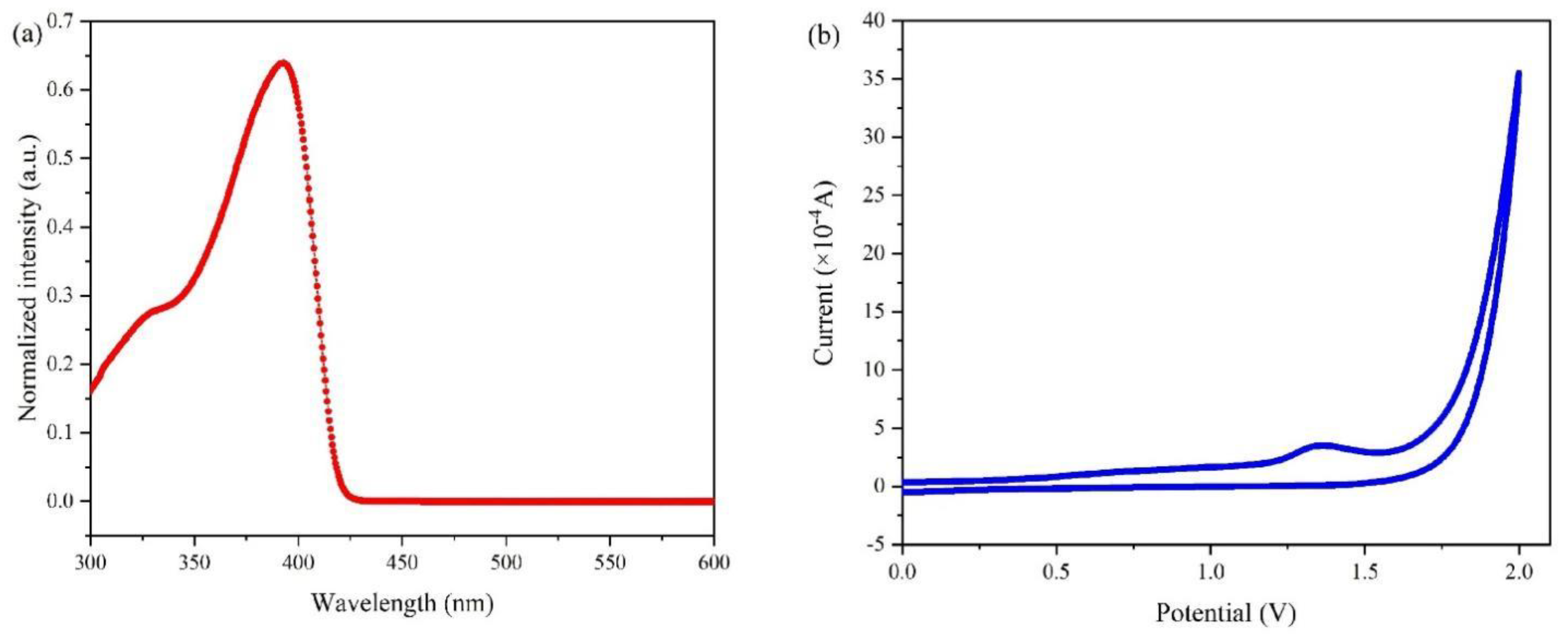
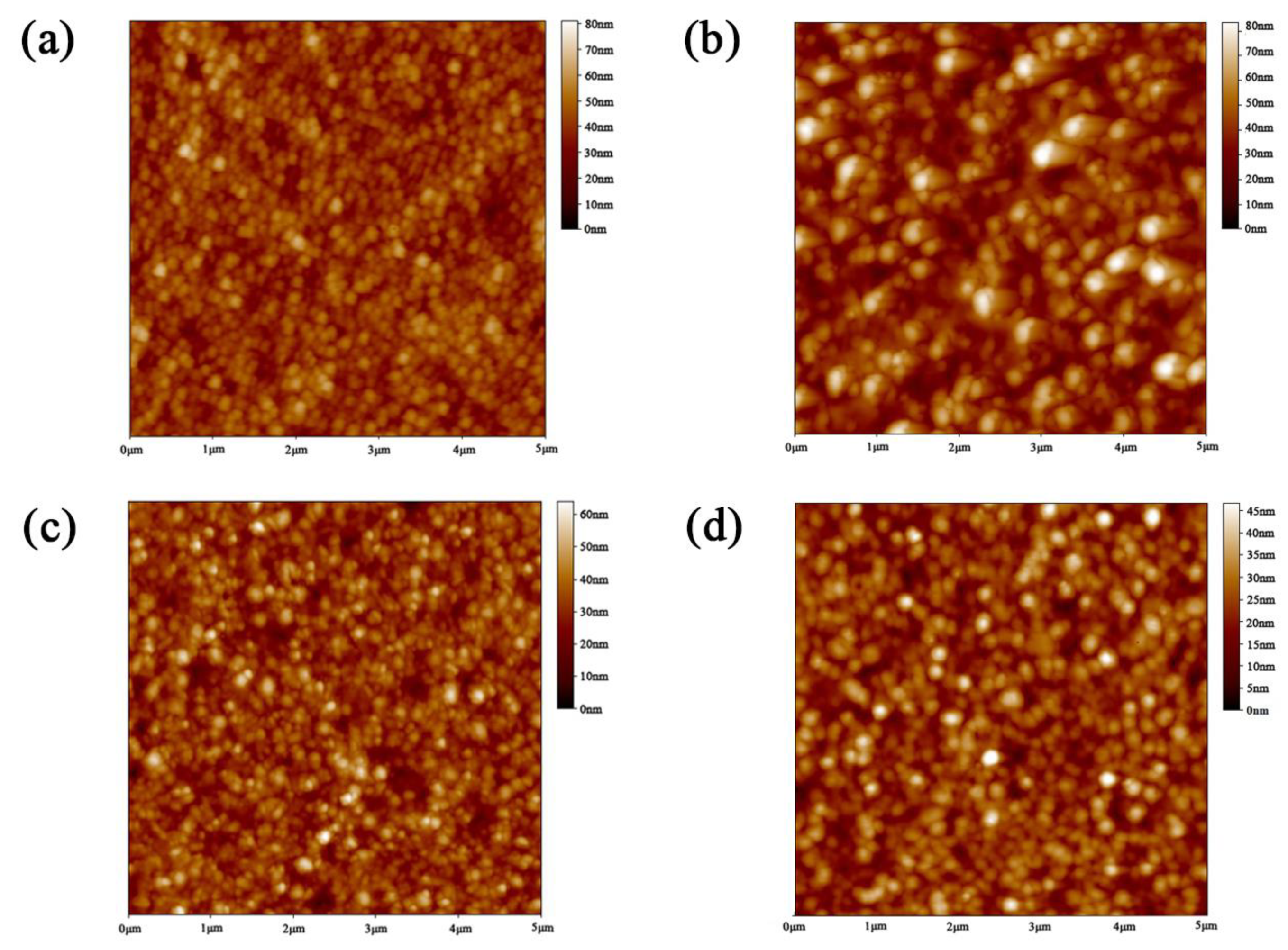
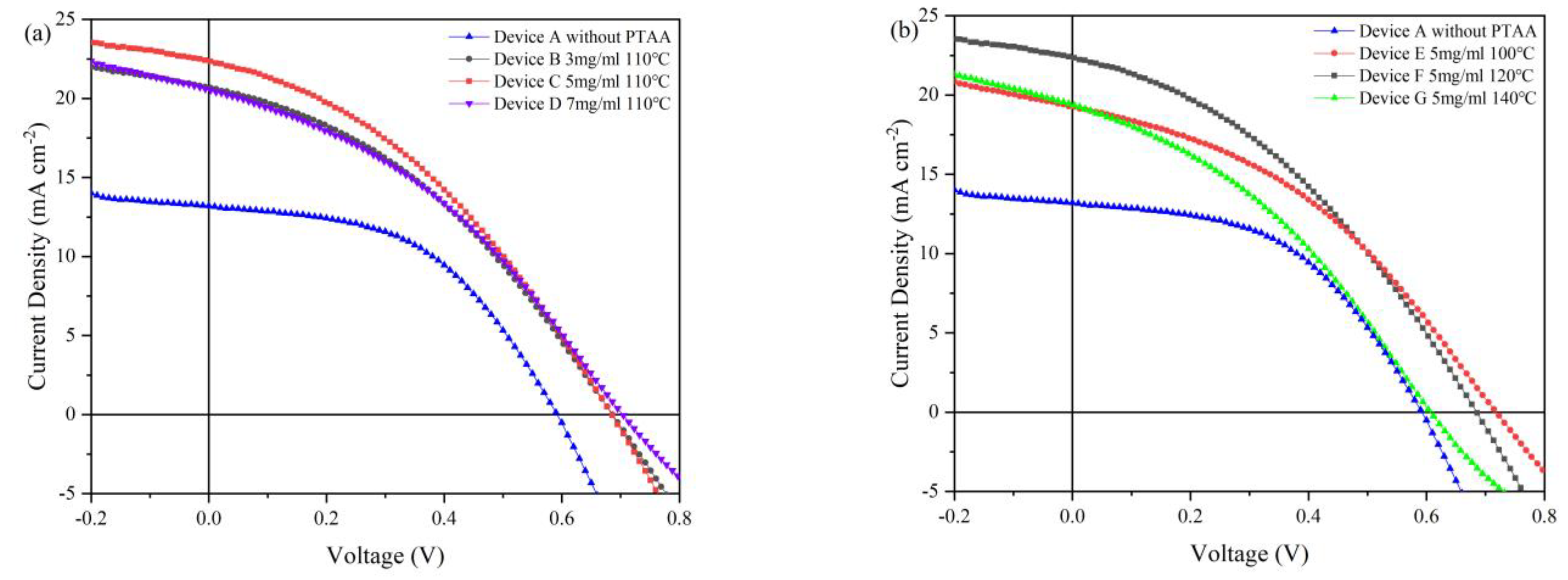
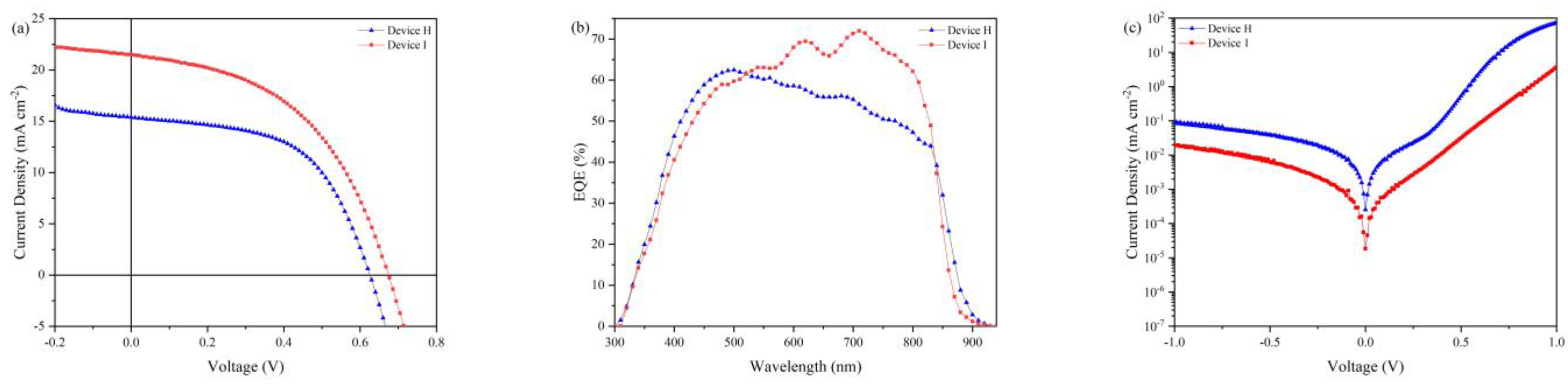
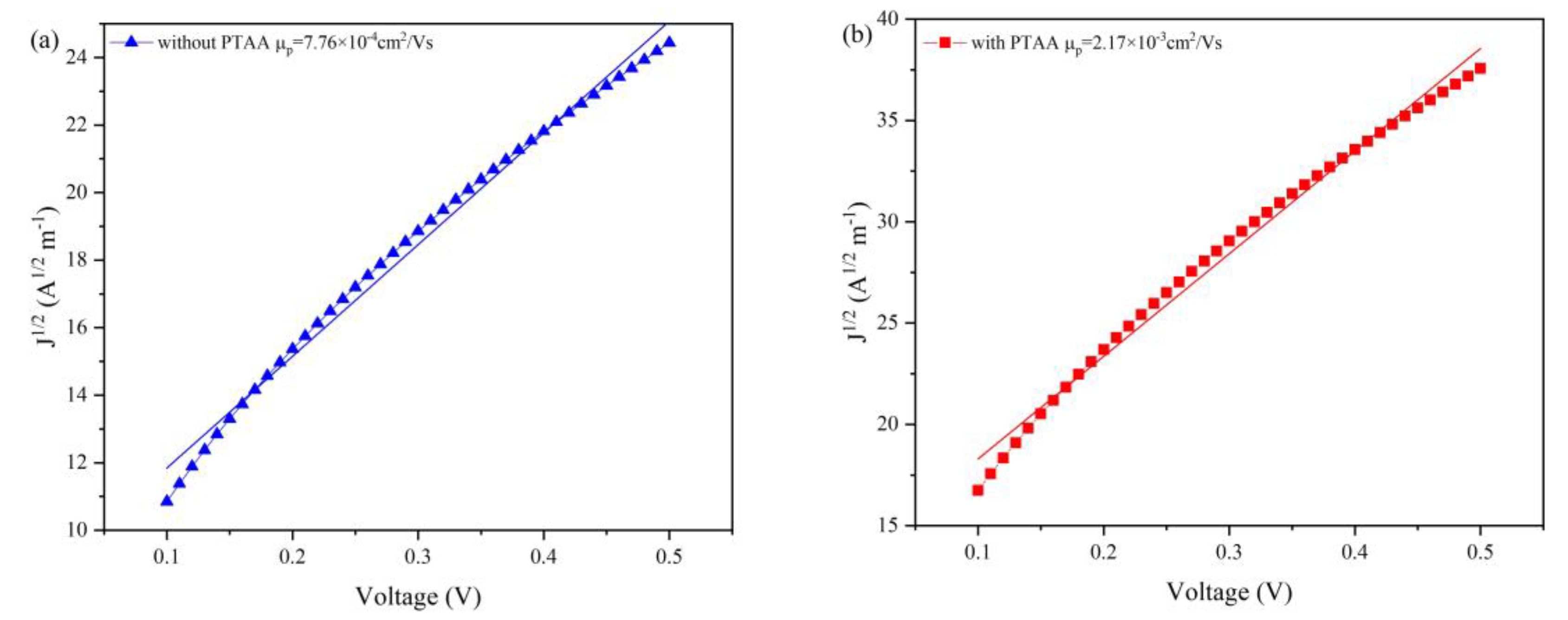
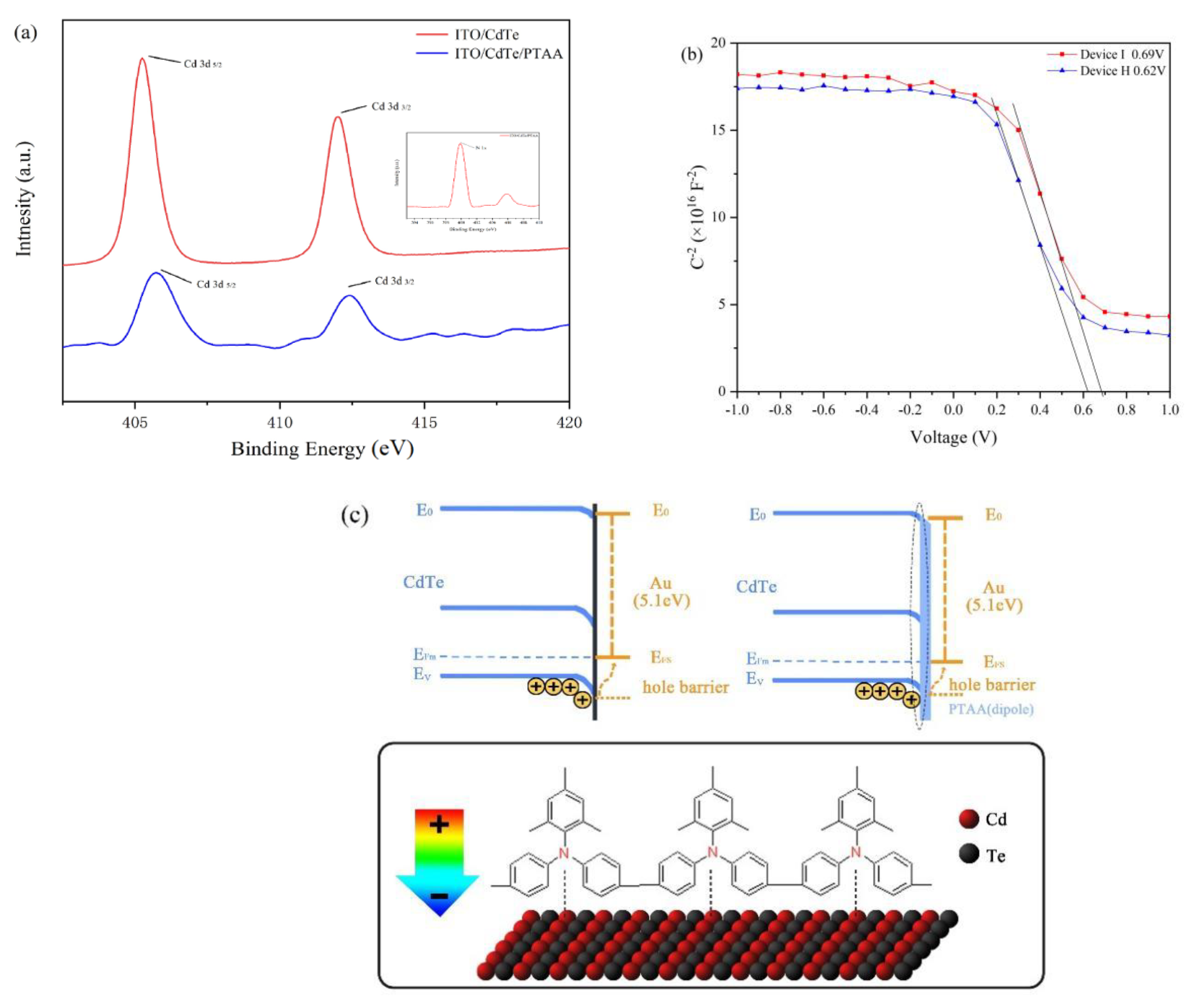
3. Results
4. Conclusions
Supplementary Materials
Author Contributions
Funding
Acknowledgments
Conflicts of Interest
References
- Jin, G.; Wei, H.; Cheng, Z.; Sun, H.; Sun, H.; Yang, B. Aqueous-processed polymer/nanocrystal hybrid solar cells with efficiency of 5.64%: The impact of device structure, polymer content, and film thickness. J. Phys. Chem. C 2017, 121, 2025–2034. [Google Scholar] [CrossRef]
- Lu, S.; Ma, W.; Jin, G.; Zeng, Q.; Feng, X.; Feng, T.; Liu, H.; Meng, S.; Redfern, S.A.T.; Yang, B. A combined experimental and theoretical investigation of donor and acceptor interface in efficient aqueous-processed polymer/nanocrystal hybrid solar cells. Sci. China-Chem. 2018, 61, 437–443. [Google Scholar] [CrossRef]
- Xue, H.; Wu, R.; Xie, Y.; Tan, Q.; Qin, D.; Wu, H.; Huang, W. Recent progress on solution-processed CdTe nanocrystals solar cells. Appl. Sci.-Basel 2016, 6, 197. [Google Scholar] [CrossRef]
- Jin, G.; Chen, N.; Zeng, Q.; Liu, F.; Yuan, W.; Xiang, S.; Feng, T.; Du, X.; Ji, T.; Wang, L.; et al. Aqueous-Processed polymer/nanocrystal hybrid solar cells with double-side bulk heterojunction. Adv. Energy Mater. 2018, 8, 1701966. [Google Scholar] [CrossRef]
- Yang, Z.; Fan, J.Z.; Proppe, A.H.; de Arquer, F.P.G.; Rossouw, D.; Voznyy, O.; Lan, X.; Liu, M.; Walters, G.; Quintero-Bermudez, R.; et al. Mixed-quantum-dot solar cells. Nat. Commun. 2017, 8, 1325. [Google Scholar] [CrossRef]
- Kim, T.; Firdaus, Y.; Kirmani, A.R.; Liang, R.-Z.; Hu, H.; Liu, M.; El Labban, A.; Hoogland, S.; Beaujuge, P.M.; Sargent, E.H.; et al. Hybrid tandem quantum dot/organic solar cells with enhanced photocurrent and efficiency via ink and interlayer engineering. ACS Energy Lett. 2018, 3, 1307–1314. [Google Scholar] [CrossRef]
- Burst, J.M.; Duenow, J.N.; Albin, D.S.; Colegrove, E.; Reese, M.O.; Aguiar, J.A.; Jiang, C.S.; Patel, M.K.; Al-Jassim, M.M.; Kuciauskas, D.; et al. CdTe solar cells with open-circuit voltage breaking the 1V barrier. Nat. Energy 2016, 1, 16015. [Google Scholar] [CrossRef]
- Swanson, D.E.; Sites, J.R.; Sampath, W.S. Co-sublimation of CdSexTe1-x layers for CdTe solar cells. Sol. Energy Mater. Sol. Cells 2017, 159, 389–394. [Google Scholar] [CrossRef]
- Kumar, S.G.; Rao, K.S.R.K. Physics and chemistry of CdTe/CdS thin film heterojunction photovoltaic devices: Fundamental and critical aspects. Energy Environ. Sci. 2014, 7, 45–102. [Google Scholar] [CrossRef]
- Zhang, H.; Kurley, J.M.; Russell, J.C.; Jang, J.; Talapin, D.V. Solution-Processed, ultrathin solar cells from CdCl3—Capped CdTe nanocrystals: The multiple roles of CdCl3-ligands. J. Am. Chem. Soc. 2016, 138, 7464–7467. [Google Scholar] [CrossRef]
- Panthani, M.G.; Kurley, J.M.; Crisp, R.W.; Dietz, T.C.; Ezzyat, T.; Luther, J.M.; Talapin, D.V. High efficiency solution processed sintered CdTe nanocrystal solar cells: The role of interfaces. Nano Lett. 2014, 14, 670–675. [Google Scholar] [CrossRef] [PubMed]
- Rong, Z.; Guo, X.; Lian, S.; Liu, S.; Qin, D.; Mo, Y.; Xu, W.; Wu, H.; Zhao, H.; Hou, L. Interface engineering for both cathode and anode enables low-cost highly efficient solution-processed CdTe nanocrystal solar cells. Adv. Funct. Mater. 2019, 29, 1904018. [Google Scholar] [CrossRef]
- Fahrenbruch, A.L. Ohmic contacts and doping of CdTe. Sol. Cells 1987, 21, 399–412. [Google Scholar] [CrossRef]
- Bastola, E.; Subedi, K.K.; Alfadhili, F.K.; Phillips, A.B.; Heben, M.J.; Ellingson, R.J.; IEEE. Room temperature processed transparent Cu-Zn-S nanocomposites as hole transport materials in CdTe photovoltaics. In Proceedings of the IEEE 46th Photovoltaic Specialists Conference (PVSC), Chicago, IL, USA, 16–21 June 2019; pp. 144–148. [Google Scholar]
- Demtsu, S.H.; Albin, D.S.; Sites, J.R.; Metzger, W.K.; Duda, A. Cu-related recombination in CdS/CdTe solar cells. Thin Solid Film. 2008, 516, 2251–2254. [Google Scholar] [CrossRef]
- Fakharuddin, A.; Schmidt-Mende, L.; Garcia-Belmonte, G.; Jose, R.; Mora-Sero, I. Interfaces in perovskite solar cells. Adv. Energy Mater. 2017, 7, 1700623. [Google Scholar] [CrossRef]
- Jeong, M.; Choi, I.W.; Go, E.M.; Cho, Y.; Kim, M.; Lee, B.; Jeong, S.; Jo, Y.; Choi, H.W.; Lee, J.; et al. Stable perovskite solar cells with efficiency exceeding 24.8% and 0.3-V voltage loss. Science 2020, 369, 1615–1620. [Google Scholar] [CrossRef] [PubMed]
- Huang, L.; Hu, Z.; Xu, J.; Zhang, K.; Zhang, J.; Zhang, J.; Zhu, Y. Efficient and stable planar perovskite solar cells with a non-hygroscopic small molecule oxidant doped hole transport layer. Electrochim. Acta 2016, 196, 328–336. [Google Scholar] [CrossRef]
- Wang, M.; Wang, H.; Li, W.; Hu, X.; Sun, K.; Zang, Z. Defect passivation using ultrathin PTAA layers for efficient and stable perovskite solar cells with a high fill factor and eliminated hysteresis. J. Mater. Chem. A 2019, 7, 26421–26428. [Google Scholar] [CrossRef]
- Kim, J.H.; Liang, P.-W.; Williams, S.T.; Cho, N.; Chueh, C.-C.; Glaz, M.S.; Ginger, D.S.; Jen, A.K.Y. High-Performance and environmentally stable planar heterojunction perovskite solar cells based on a solution-processed copper-doped nickel oxide hole-transporting layer. Adv. Mater. 2015, 27, 695–701. [Google Scholar] [CrossRef]
- Jung, J.W.; Chueh, C.-C.; Jen, A.K.Y. A Low-Temperature, Solution-Processable, Cu-doped nickel oxide hole-transporting layer via the combustion method for high-performance thin-film perovskite solar cells. Adv. Mater. 2015, 27, 7874–7880. [Google Scholar] [CrossRef]
- Han, Q.; Hsieh, Y.-T.; Meng, L.; Wu, J.-L.; Sun, P.; Yao, E.-P.; Chang, S.-Y.; Bae, S.-H.; Kato, T.; Bermudez, V.; et al. High-performance perovskite/Cu(In,Ga)Se-2 monolithic tandem solar cells. Science 2018, 361, 904–908. [Google Scholar] [CrossRef] [PubMed]
- Burschka, J.; Dualeh, A.; Kessler, F.; Baranoff, E.; Cevey-Ha, N.-L.; Yi, C.; Nazeeruddin, M.K.; Graetzel, M. Tris(2-(1H-pyrazol-1-yl)pyridine)cobalt(III) as p-Type dopant for organic semiconductors and its application in highly efficient solid-state dye-sensitized solar cells. J. Am. Chem. Soc. 2011, 133, 18042–18045. [Google Scholar] [CrossRef] [PubMed]
- Xu, B.; Sheibani, E.; Liu, P.; Zhang, J.; Tian, H.; Vlachopoulos, N.; Boschloo, G.; Kloo, L.; Hagfeldt, A.; Sun, L. Carbazole-Based hole-transport materials for efficient solid-state dye-sensitized solar cells and perovskite solar cells. Adv. Mater. 2014, 26, 6629–6634. [Google Scholar] [CrossRef] [PubMed]
- Wang, Y.-K.; Yuan, Z.-C.; Shi, G.-Z.; Li, Y.-X.; Li, Q.; Hui, F.; Sun, B.-Q.; Jiang, Z.-Q.; Liao, L.-S. Dopant-Free spiro-triphenylamine/fluorene as hole-transporting material for perovskite solar cells with enhanced efficiency and stability. Adv. Funct. Mater. 2016, 26, 1375–1381. [Google Scholar] [CrossRef]
- Rombach, F.M.; Haque, S.A.; Macdonald, T.J. Lessons learned from spiro-OMeTAD and PTAA in perovskite solar cells. Energy Environ. Sci. 2021, 14, 5161–5190. [Google Scholar] [CrossRef]
- Du, X.; Chen, Z.; Liu, F.; Zeng, Q.; Jin, G.; Li, F.; Yao, D.; Yang, B. Improvement in open-circuit voltage of thin film solar cells from aqueous nanocrystals by interface engineering. ACS Appl. Mater. Interfaces 2016, 8, 900–907. [Google Scholar] [CrossRef]
- Jiang, Y.; Pan, Y.; Wu, W.; Luo, K.; Rong, Z.; Xie, S.; Zuo, W.; Yu, J.; Zhang, R.; Qin, D.; et al. Hole transfer layer engineering for CdTe nanocrystal photovoltaics with improved efficiency. Nanomaterials 2020, 10, 1348. [Google Scholar] [CrossRef]
- Guo, X.; Rong, Z.; Wang, L.; Liu, S.; Liu, Z.; Luo, K.; Chen, B.; Qin, D.; Ma, Y.; Wu, H.; et al. Surface passivation via acid vapor etching enables efficient and stable solution-processed CdTe nanocrystal solar cells. Sustain. Energy Fuels 2020, 4, 399–406. [Google Scholar] [CrossRef]
- Cheng, M.; Aitola, K.; Chen, C.; Zhang, F.; Liu, P.; Sveinbjornsson, K.; Hua, Y.; Kloo, L.; Boschloo, G.; Sun, L. Acceptor Donor Acceptor type ionic molecule materials for efficient perovskite solar cells and organic solar cells. Nano Energy 2016, 30, 387–397. [Google Scholar] [CrossRef]
- Zhang, J.; Zhang, T.; Jiang, L.; Bach, U.; Cheng, Y.-B. 4-tert-Butylpyridine free hole transport materials for efficient perovskite solar cells: A new strategy to enhance the environmental and thermal stability. ACS Energy Lett. 2018, 3, 1677–1682. [Google Scholar] [CrossRef]
- Seo, J.-Y.; Kim, H.-S.; Akin, S.; Stojanovic, M.; Simon, E.; Fleischer, M.; Hagfeldt, A.; Zakeeruddin, S.M.; Graetzel, M. Novel p-dopant toward highly efficient and stable perovskite solar cells. Energy Environ. Sci. 2018, 11, 2985–2992. [Google Scholar] [CrossRef]
- Liu, Z.; Krueckemeier, L.; Krogmeier, B.; Klingebiel, B.; Marquez, J.A.; Levcenko, S.; Oez, S.; Mathur, S.; Rau, U.; Unold, T.; et al. Open-Circuit voltages exceeding 1.26 V in planar methylammonium lead iodide perovskite solar cells. ACS Energy Lett. 2019, 4, 110–117. [Google Scholar] [CrossRef]
- Liu, S.; Liu, W.; Heng, J.; Zhou, W.; Chen, Y.; Wen, S.; Qin, D.; Hou, L.; Wang, D.; Xu, H. Solution-Processed efficient nanocrystal solar cells based on CdTe and CdS nanocrystals. Coatings 2018, 8, 26. [Google Scholar] [CrossRef]
- Liu, H.; Tian, Y.; Zhang, Y.; Gao, K.; Lu, K.; Wu, R.; Qin, D.; Wu, H.; Peng, Z.; Hou, L.; et al. Solution processed CdTe/CdSe nanocrystal solar cells with more than 5.5% efficiency by using an inverted device structure. J. Mater. Chem. C 2015, 3, 4227–4234. [Google Scholar] [CrossRef]
- Wen, S.; Li, M.; Yang, J.; Mei, X.; Wu, B.; Liu, X.; Heng, J.; Qin, D.; Hou, L.; Xu, W.; et al. Rationally controlled synthesis of CdSexTe1-x alloy nanocrystals and their application in efficient graded bandgap solar cells. Nanomaterials 2017, 7, 380. [Google Scholar] [CrossRef]
- Xie, Y.; Tan, Q.; Zhang, Z.; Lu, K.; Li, M.; Xu, W.; Qin, D.; Zhang, Y.; Hou, L.; Wu, H. Improving performance in CdTe/CdSe nanocrystals solar cells by using bulk nano-heterojunctions. J. Mater. Chem. C 2016, 4, 6483. [Google Scholar] [CrossRef]
- Ciach, R.; Dotsenko, Y.P.; Naumov, V.V.; Shmyryeva, A.N.; Smertenko, P.S. Injection technique for the study of solar cell test structures. Sol. Energy Mater. Sol. Cells 2003, 76, 613–624. [Google Scholar] [CrossRef]
- Feng, Z.C.; Chou, H.C.; Rohatgi, A.; Lim, G.K.; Wee, A.T.S.; Tan, K.L. Correlations between CdTe/CdS/SnO2/glass solar cell performance and the interface/surface properties. J. Appl. Phys. 1996, 79, 2151–2153. [Google Scholar] [CrossRef]
- Rong, Y.; Hu, Y.; Mei, A.; Tan, H.; Saidaminov, M.I.; Seok, S.I.; McGehee, M.D.; Sargent, E.H.; Han, H. Challenges for commercializing perovskite solar cells. Science 2018, 361, eaat8235. [Google Scholar] [CrossRef]
- Hawash, Z.; Ono, L.K.; Qi, Y. Recent advances in spiro-MeOTAD hole transport material and its applications in organic-inorganic halide perovskite solar cells. Adv. Mater. Interfaces 2018, 5, 1700623. [Google Scholar] [CrossRef] [Green Version]
- Zhu, J.; Yang, Y.; Gao, Y.; Qin, D.; Wu, H.; Hou, L.; Huang, W. Enhancement of open-circuit voltage and the fill factor in CdTe nanocrystal solar cells by using interface materials. Nanotechnology 2014, 25, 365203. [Google Scholar] [CrossRef] [PubMed]


| Device | VOC (V) | JSC (mA cm−2) | FF (%) | PCE (%) |
|---|---|---|---|---|
| A | 0.58 | 14.61 | 42.28 | 3.58 |
| B | 0.67 | 20.32 | 36.87 | 5.00 |
| C | 0.68 | 21.06 | 37.40 | 5.41 |
| D | 0.70 | 21.54 | 35.38 | 5.29 |
| E | 0.71 | 19.26 | 39.26 | 5.40 |
| F | 0.69 | 22.33 | 37.17 | 5.70 |
| G | 0.60 | 19.35 | 36.44 | 4.25 |
| H | 0.62 | 15.41 | 55.96 | 5.34 |
| I | 0.68 | 21.47 | 47.81 | 6.95 |
| Thin Film | N 1s | P 2p | Cd 3d3/2 | Cd 3d5/2 |
|---|---|---|---|---|
| CdTe | - | 133.12 | 412.01 | 405.13 |
| CdTe/PTAA | 399.82 | 133.71 | 412.60 | 405.72 |
Publisher’s Note: MDPI stays neutral with regard to jurisdictional claims in published maps and institutional affiliations. |
© 2022 by the authors. Licensee MDPI, Basel, Switzerland. This article is an open access article distributed under the terms and conditions of the Creative Commons Attribution (CC BY) license (https://creativecommons.org/licenses/by/4.0/).
Share and Cite
Xu, A.; Huang, Q.; Luo, K.; Qin, D.; Xu, W.; Wang, D.; Hou, L. Efficient Nanocrystal Photovoltaics with PTAA as Hole Transport Layer. Nanomaterials 2022, 12, 3067. https://doi.org/10.3390/nano12173067
Xu A, Huang Q, Luo K, Qin D, Xu W, Wang D, Hou L. Efficient Nanocrystal Photovoltaics with PTAA as Hole Transport Layer. Nanomaterials. 2022; 12(17):3067. https://doi.org/10.3390/nano12173067
Chicago/Turabian StyleXu, Ao, Qichuan Huang, Kaiying Luo, Donghuan Qin, Wei Xu, Dan Wang, and Lintao Hou. 2022. "Efficient Nanocrystal Photovoltaics with PTAA as Hole Transport Layer" Nanomaterials 12, no. 17: 3067. https://doi.org/10.3390/nano12173067