Article

Influence of Grain Boundary Scattering on the Field-Effect Mobility of Solid-Phase Crystallized Hydrogenated Polycrystalline In2O3 (In2O3:H)

1
Graduate School of Natural Science and Technology, Shimane University, 1060 Nishikawatsu, Matsue 690-8504, Japan
2
Japan Synchrotron Radiation Research Institute (JASRI/SPring-8), 1-1-1 Kouto, Sayo 679-5198, Japan
3
School of Environmental Science and Engineering and Research Institute, Kochi University of Technology, 185 Miyanokuchi, Tosayamada, Kami 782-8502, Japan
*
Author to whom correspondence should be addressed.
Nanomaterials 2022, 12(17), 2958; https://doi.org/10.3390/nano12172958
Submission received: 15 July 2022 / Revised: 15 August 2022 / Accepted: 24 August 2022 / Published: 26 August 2022
(This article belongs to the Section Nanoelectronics, Nanosensors and Devices)

Abstract

:
Hydrogenated polycrystalline In2O3 (In2O3:H) thin-film transistors (TFTs) fabricated via the low-temperature solid-phase crystallization (SPC) process with a field-effect mobility (μFE) exceeding 100 cm2 V−1 s−1 are promising candidates for future electronics applications. In this study, we investigated the effects of the SPC temperature of Ar + O2 + H2-sputtered In2O3:H films on the electron transport properties of In2O3:H TFTs. The In2O3:H TFT with an SPC temperature of 300 °C exhibited the best performance, having the largest µFE of 139.2 cm2 V−1 s−1. In contrast, the µFE was slightly degraded with increasing SPC temperature (400 °C and higher). Extended X-ray absorption fine structure analysis revealed that the medium-range ordering in the In2O3:H network was further improved by annealing up to 600 °C, while a large amount of H2O was desorbed from the In2O3:H films at SPC temperatures above 400 °C, resulting in the creation of defects at grain boundaries. The threshold temperature of H2O desorption corresponded well with the carrier transport properties; the µFE of the TFTs started to deteriorate at SPC temperatures of 400 °C and higher. Thus, it was suggested that the hydrogen remaining in the film after SPC plays an important role in the passivation of electron traps, especially for grain boundaries, resulting in an enhancement of the µFE of In2O3:H TFTs.

1. Introduction

Amorphous oxide semiconductors (AOSs), represented by amorphous In–Ga–Zn–O (a-IGZO), have now become standard channel materials in thin-film transistors (TFTs) for active-matrix liquid-crystal displays and active-matrix organic light-emitting diode displays [1,2,3]. This is because a-IGZO has properties that are superior to hydrogenated amorphous Si (a-Si:H), such as a large field-effect mobility (μFE) of over 10 cm2 V−1 s−1, an extremely low leakage current, a low processing temperature (<350 °C), and excellent uniformity [4,5,6,7,8,9,10,11,12]. Although the μFE value of a-IGZO TFTs is more than ten times higher than that of a-Si:H TFTs (<1 cm2 V−1 s−1), the further improvement of μFE values is required to expand their range of applications as alternatives to poly-Si TFTs (50–100 cm2 V−1 s−1) [13]. The optimization of AOS composition is one approach for improving μFE; for example, an increase in the In ratio due the considerable spatial spread of the In 5s orbital with a large overlap can provide a facile electron transport path with a low electron effective mass [14,15]. Although various compositions, including In–Sn–Zn–O [16,17], In–W–Zn–O [18,19], Al–In–Sn–Zn–O [20], and In–Ga–Zn–Sn–O [21], have been proposed to enhance the μFE, the value remains insufficiently high to compete with that of low-temperature polysilicon (LTPS) TFTs [22].
In contrast, the crystallization of OSs is an another approach for improving μFE, because the subgap density of states originating from structural disorder and defects can be suppressed via lattice ordering. Although polycrystalline Oss, including In2O3, ZnO, and SnO2, have been investigated as channel materials in early oxide-based TFTs [23,24,25], they can easily create oxygen vacancies, leading to degenerate semiconductors. In addition, µFE degradation due to grain boundary scattering is a serious issue for polycrystalline OSs as well as poly-Si [26,27]. Polycrystalline In2O3 films have been investigated for use as the transparent conductive oxide (TCO) in solar cells. Koida et al. reported a degenerate hydrogen-doped polycrystalline In2O3 (In2O3:H) film with high electron mobility (100–130 cm2 V−1 s−1) produced by solid-phase crystallization (SPC) [28]. Recently, we reported a μFE value of 139.2 cm2 V−1 s−1 for a TFT obtained using hydrogenated polycrystalline In2O3 (In2O3:H) formed via SPC at 300 °C [29]. The obtained μFE value is comparable to the Hall mobility of single-crystalline epitaxial In2O3 films (~160 cm2 V−1 s−1) [30]. The as-deposited amorphous In2O3:H was converted into a polycrystalline film with lateral grain sizes of about 140 nm via SPC [29]. However, the effects of SPC temperature on the electrical and structural properties of In2O3:H films are not yet understood in detail.
In this study, we investigated the effects of SPC temperature on electron transport properties in In2O3:H films and TFTs. Hydrogen intentionally doped during sputtering was found to play an essential role in the passivation of defects, especially for the grain boundaries of the films, resulting in an enhanced μFE of the TFTs.

2. Materials and Methods

2.1. Fabrication of In2O3:H TFTs

In2O3:H TFTs were fabricated on a heavily doped p-type Si substrate with a 100 nm thick thermally grown SiO2 layer. The doped p-type Si substrate and SiO2 layer were used as the gate electrode and gate insulator, respectively. The 30 nm thick In2O3:H channels were deposited via pulsed direct current (DC) magnetron sputtering, without substrate heating, from a ceramic In2O3 target using a mixture of Ar, O2, and H2 gases. The gas flow ratios of O2 (R[O2] = O2/(Ar + O2 + H2)) and H2 (R[H2] = H2/(Ar + O2 + H2)) were 1% and 5%, respectively. The deposition pressure and DC power were maintained at 0.6 Pa and 50 W, respectively. The base pressure before gas introduction was below 6 × 10⁻⁵ Pa. After deposition, the In2O3:H films were annealed in ambient air at a temperature range of 200–600 °C for 1 h. After annealing, a 100 nm thick SiO2 film was deposited via reactive sputtering without substrate heating. Subsequently, Al source/drain electrodes were deposited via sputtering. Finally, the In2O3:H TFTs were annealed at 250 °C in ambient air for 1 h. In2O3:H, SiO2, and Al films were deposited through a shadow mask, and both the channel length and width were 300 µm.

2.2. Characterization Methods

The carrier concentration (Ne) and Hall mobility (µFE) of the In2O3:H films were determined by Hall effect measurements (Accent, HL5500PC) using the van der Pauw geometry at room temperature. The local structural changes of the films were evaluated through extended X-ray absorption fine structure (EXAFS) at the BL01B1 beamline in SPring-8. The In K-edge fluorescence XAFS of the films was measured using a 19-element Ge detector with an incident X-ray angle of 2° with respect to the sample surface. The XAFS data were analyzed using the Demeter software packages [31]. The macroscopic structure of the In2O3:H films was observed using electron backscattering diffraction (EBSD) (EDAX-TSL Hikari High-Speed EBSD Detector). The hydrogen concentration in the films was measured using secondary ion mass spectrometry (SIMS) (ULVAC-PHI, ADEPT-1010) with Cs+ as a primary ion. The chemical bonding states of the constituent elements and hydrogen were evaluated from their thermal effusion using thermal desorption spectroscopy (TDS), which was carried out while varying the stage temperature from 50 to 800 °C at a heating rate of 60 °C min−1. Reference films of In2O3 under similar conditions maintaining an R[H2] of 0% (without hydrogen introduction) were deposited for comparison.

3. Results and Discussion

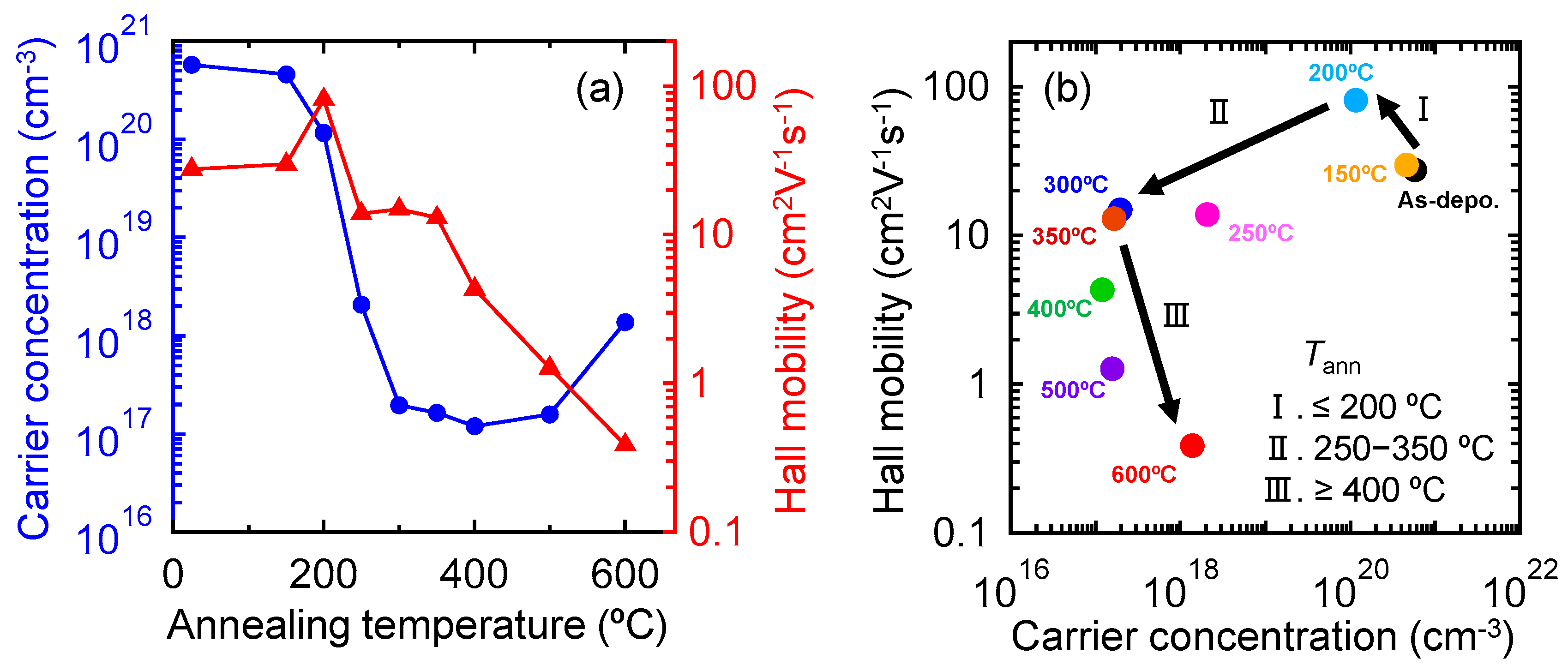
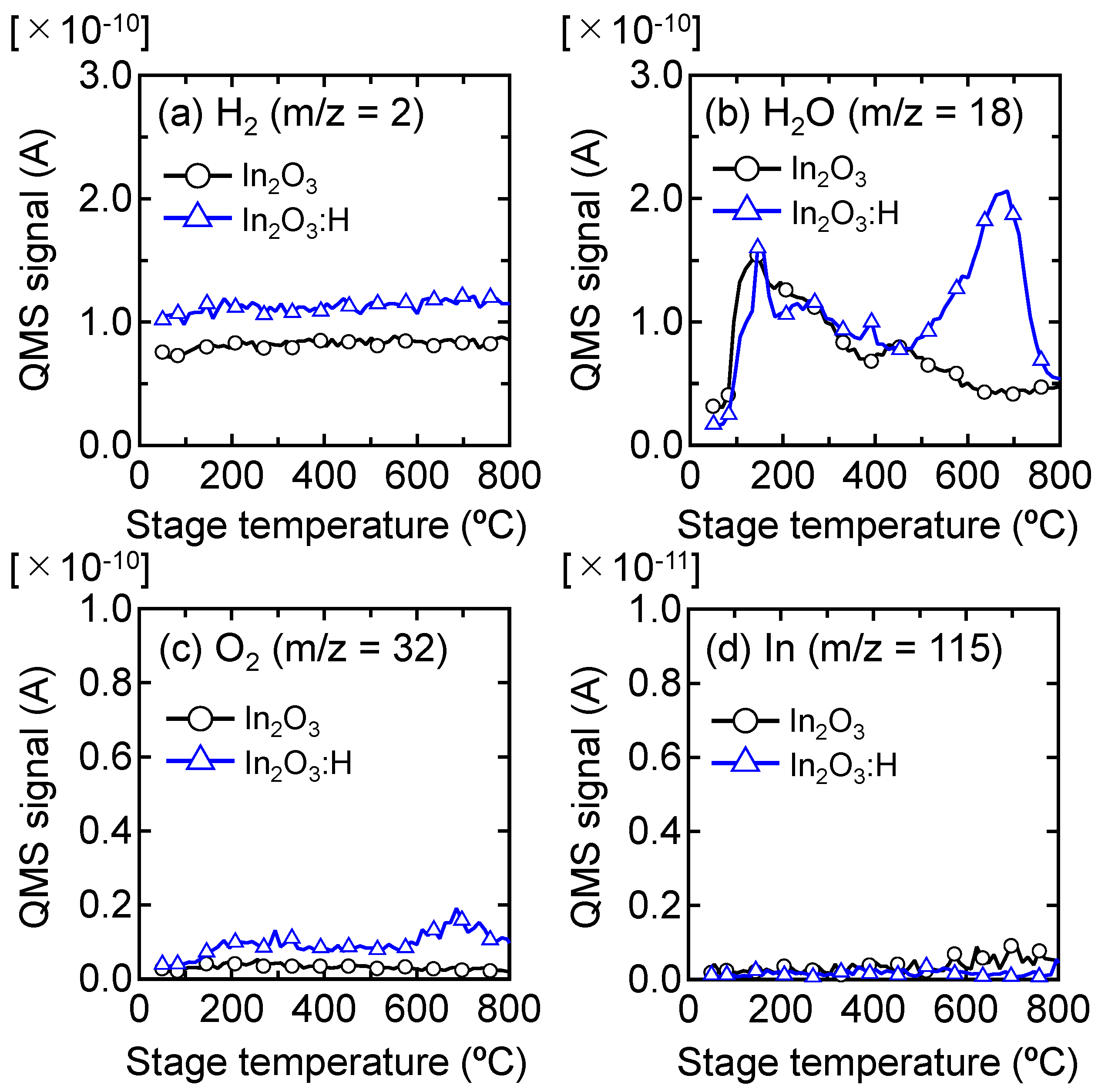
3.1. Electrical Properties of In2O3:H Films

Figure 1a shows the variations in Ne and µH in the 50 nm thick In2O3:H films as a function of the annealing temperature (Tann). The Ne of the as-deposited film (5.7 × 1020 cm−3) began to decrease rapidly from Tann = 200 °C, where SPC occurred. Then, the In2O3:H exhibited an almost constant Ne of ~2 × 1017 cm−3 (an appropriate value for TFT fabrication) over a Tann range of 300–500 °C. After reaching a Tann of 600 °C, the Ne slightly increased to 1.4 × 1018 cm−3. The µH of In2O3:H increased to 78.6 cm2 V−1 s−1 after SPC occurred (Tann = 200 °C), whereas the µH of the films decreased to ~15 cm2 V−1 s−1 at a Tann range of 250–350 °C. As Tann further increased, the µH of In2O3:H began to decrease, resulting in a µH of 0.4 cm2 V−1 s−1 at Tann = 600 °C.
To understand the carrier transport properties of the In2O3:H films, the relationship between µH and Ne for the films with various Tann values is shown in Figure 1b. The changes in electrical properties could be classified into the following three regions: (I) enhanced µH at a Tann ≤ 200 °C; (II) decreased µH with decreasing Ne at Tann = 250–350 °C; and (III) decreased µH with constant or increasing Ne at Tann ≥ 400 °C. The decrease in the µH of the polycrystalline In2O3:H films with increasing Tann in regions II and III was considered to be due to the effects of grain boundary scattering and intragrain scattering. In general, for degenerate transparent conducting oxide materials, the mobility in the grains is determined by an optical method using the Drude model, because optical mobilities are not affected by grain boundary scattering [32,33]. However, it is difficult to determine the optical mobility of In2O3:H films annealed at Tann ≥ 250 °C because the free electrons are significantly decreased to the order of 1017 cm−3 and the films become non-degenerate semiconductors [34,35]. Therefore, we evaluated the effects of intragrain scattering by measuring the field-effect mobility of In2O3:H TFTs. This is because when a voltage is applied to the gate, a large number of carriers (1019–1020 cm−3) are accumulated at the In2O3:H/gate insulator interface, and the effects of grain boundary scattering can almost be neglected since electrons tunnel through the narrow width (<1 nm) of the grain barriers at high Ne values [36].

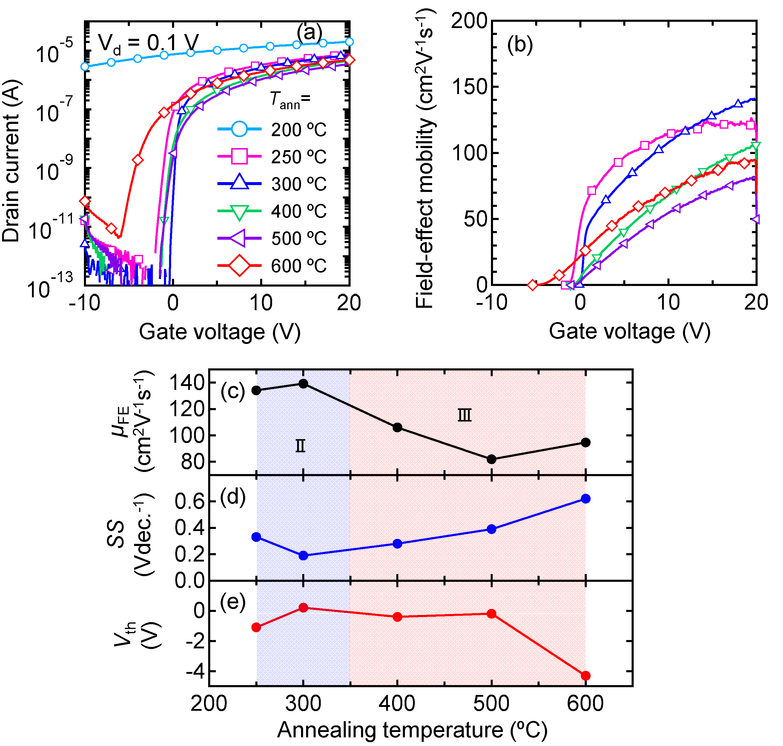
3.2. Electrical Properties of In2O3:H TFTs

Figure 2 shows the typical characteristics of the In2O3:H TFTs annealed at Tann values of 200–600 °C. The µFE was calculated from the linear transfer characteristics (Vds = 0.1 V) using the following equation:
μ FE = L g m W C ox V ds
where gm is the transconductance, Cox is the oxide capacitance of the gate insulator, and Vds is the drain voltage. Vth was defined by gate voltage (Vgs) at a drain current (Ids) of 1 nA, and SS was extracted from Vgs, which required an increase in the Ids from 10 to 100 pA. The average values and standard deviations (σ) of the characteristics of five TFTs on the same substrate are shown in Supplementary Figure S1 and Supplementary Table S1. The In2O3:H TFT annealed at 200 °C did not exhibit any switching (conductive behavior) because the In2O3:H film was still in a degenerated state (Ne = 5.7 × 1020 cm−3). The TFTs annealed at 300 °C exhibited the best performance, with the largest field-effect mobility (µFE) of 139.2 cm2 V−1 s−1 and smallest subthreshold swing (SS) of 0.19 Vdec−1 with an appropriate threshold voltage (Vth) of 0.2 V (shown in Figure 2c,e). Although the µH of the In2O3:H films decreased to 14.9 cm2 V−1 s−1 with a Ne of 2.0 × 1017 cm−3 after annealing at 300 °C, as shown in Figure 1, extremely high µFE values were obtained from the TFTs at higher gate voltages (Figure 2b). Thus, we concluded that the decrease in µH in region II shown in Figure 1b) was mainly due to an increase in the potential barrier at the grain boundary caused by a decrease in Ne, rather than a decrease in intragrain mobility. In contrast, the TFT characteristics were slightly degraded when Tann was increased to 600 °C, i.e., the µFE decreased and the SS value increased. Comparing µH and µFE after Tann = 600 °C, the µH significantly deteriorated to 0.4 cm2 V−1 s−1, whereas the µFE of the TFTs was maintained at 94.6 cm2 V−1 s−1. This result suggests that grain boundary scattering is a dominant factor that limits the µH in films annealed at 400 °C and higher.

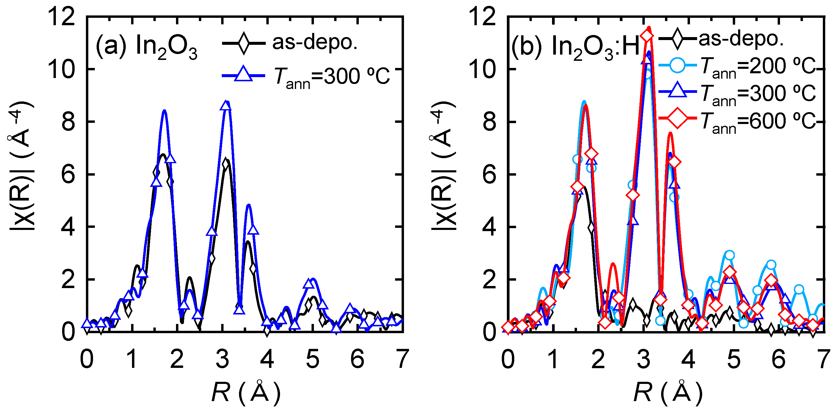
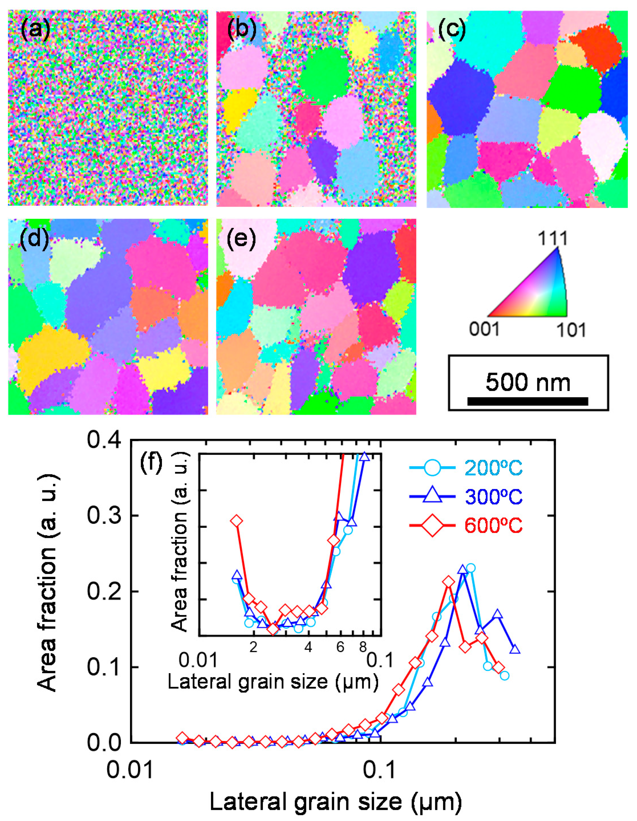
3.3. Structural Properties of In2O3:H Films

To investigate the crystallinity of the films, the effect of Tann on the local structure of the In2O3:H films was evaluated using XAFS. Figure 3 shows Fourier-transformed (FT) EXAFS spectra of the In K-edge for the (a) In2O3 and (b) In2O3:H films as a function of the phase uncorrected interatomic distance. The as-deposited In2O3 film without hydrogen introduction during sputtering exhibited three obvious peaks (Figure 3a), which corresponded to the nearest oxygen (In–O) and the second and third nearest In (In–In and In–In*). Using the values for the crystalline In2O3 powder standard, the interatomic distance (R) and Debye–Waller factor (σ2) for the films were determined. The k-range of the EXAFS data used in the analyses was k = 3–14 Å−1 with a k-weight of 3. The fitting carried out in the R space was from R = 1.0–4.0 Å for the three-shell model. As shown in Table 1, the RIn–O, RIn–In, and RIn–In* values of the as-deposited In2O3 film without hydrogen were 2.16, 3.35, and 3.82 Å, respectively, which agreed well with the interatomic distance of the In2O3 bixbyite structure (space group Ia3, number 206) [37,38,39]. When the In2O3 film was annealed at 300 °C, no noticeable changes in R were observed (Figure 3a), while the peak intensity increased in each spectrum, resulting in a decrease in σ2. This result indicates that thermal annealing improved the structural disorder of the films. By introducing hydrogen during sputtering, the second and third nearest peaks disappeared in the as-deposited In2O3:H film, while the intensity of the first nearest peak decreased (Figure 3b), resulting in an increase in σ2In–O to 0.0112. In contrast, after annealing at 200 °C, the intensities of all peaks increased significantly and the intensities of the second and third nearest peaks were higher than those of the In2O3 film annealed at 300 °C. These results indicate that medium-range ordering was lost around In in the initial In2O3:H film, whereas medium-range ordering at distances equal to or longer than the second neighbor significantly improved after annealing at 200 °C. This is in agreement with a previous study using electron backscatter diffraction which confirmed that the amorphous state of the initial In2O3:H film and the grain size of the In2O3:H film were enlarged through SPC [29]. Therefore, the increase in µH after annealing at 200 °C, as shown in Figure 1b) (region I), is due to an increase in grain size as well as the improvement of the local structural order of the In2O3:H films. As Tann increased from 200 to 300 °C, the intensity of the first nearest peak was constant, while the intensities of the second and third nearest peaks increased slightly, resulting in a decrease in σ2In–In (0.0056) and σ2In–In (0.0049). This result indicates that the medium-range ordering was improved by annealing at 300 °C, which is in good agreement with the high intragrain mobility obtained via µFE for the In2O3:H TFT annealed at 300 °C. As Tann increased from 300 to 600 °C, the intensities of the second and third nearest peaks further increased, whereas R remained almost constant. Despite the improvement in the crystallinity of the In2O3:H films observed when annealing at 600 °C, the µFE of the TFTs slightly decreased to 94.6 cm2 V−1 s−1, as shown in Figure 2c, and the µH significantly deteriorated to 0.4 cm2 V−1 s−1. The deterioration of the µH of the In2O3:H films (Figure 1b, Region III) and the µFE of the TFTs annealed at ≥400 °C could not be explained by local structural changes in the In2O3:H films. Thus, it was suggested that the decreases in the µH and the µFE of the TFTs in region III shown in Figure 1b and Figure 2c were mainly due to the formation of defects at grain boundaries.
To investigate the origin of the deterioration of the µH of In2O3:H films at Tann ≥ 400 °C, we performed EBSD measurements. Figure 4a–e depicts the EBSD images along the normal direction for the In2O3:H films with various Tann values. The as-deposited amorphous In2O3:H film was converted into a polycrystalline In2O3:H film with grain structure embedded in the amorphous matrix at a Tann of 150 °C (Figure 4b). At a Tann of 200 °C (Figure 4c), the film was fully crystallized with a grain size of around 200 nm. After that, no significant difference was observed in the crystal grain size with increasing Tann values up to 600 °C. The corresponding area fractions of the crystalline phase are shown in Figure 4f. All films showed a maximum area fraction for a grain size of ~200 nm; however, a small proportion of the area fraction with a grain size of ~15 nm was increased in the In2O3:H film annealed at 600 °C, as shown in the insets of Figure 4f. Moreover, these small domains were located in between the large grains, as shown in Figure 4e. The results indicate that when the In2O3:H films were annealed at 400 °C and higher, small domains were created at grain boundaries that served as electron traps, resulting in a decrease in the µH in region III shown in Figure 1b.
To understand the mechanism of structural deterioration at the grain boundaries of In2O3:H films at Tann ≥ 400 °C, we performed TDS measurements. Figure 5 shows the TDS spectra of H2, H2O, O2, and In for the In2O3 and In2O3:H films. We first note that H2, O2, and In desorption were negligible for both types of films, while the H2O desorption was high for the In2O3:H film in particular. Large amounts of H2O were desorbed at a stage temperature of 400–800 °C for the In2O3:H film (Figure 5b). The amount of hydrogen in the film was quantitatively evaluated using SIMS, and it was found that 2.6 × 1021 cm−3 of hydrogen remained in the film after SPC at 300 °C, which was one order of magnitude higher than that of the In2O3 film. The H2O desorption temperature (400 °C) for the In2O3:H film corresponded well to a Tann of 400 °C, at which the µH of the films started to degrade. During annealing at a Tann of 400 °C and higher, H or –OH inside grains may migrate to grain boundaries and react with a neighboring H at the boundary, resulting in the generation of H2O molecules. As a consequence, defects are formed at grain boundaries. In other words, the presence of H and/or –OH bonds in the In2O3:H film after SPC plays an important role in the passivation of defects, especially for grain boundaries. In general, the SS value of a TFT is strongly affected by defects near the semiconductor Fermi level [2,12]. We recently reported from hard X-ray photoelectron spectroscopy analysis that intentionally introduced hydrogen is effective in reducing defects near the Fermi level in amorphous IGZO [40,41,42,43,44]. The SS values of the In2O3:H TFTs, shown in Figure 2d, increased at a Tann of 400 °C and higher, indicating defect creation. Thus, we believe that the H and/or –OH bonds remained in the films after SPC passivated the defects near the Fermi level, leading to the high µFE and steep SS values of the In2O3:H TFT annealed at 300 °C. Thus, it is worth noting that grain boundary scattering, which is a serious issue for polycrystalline Si TFTs, may not have a strong influence on the µFE of polycrystalline In2O3:H TFTs.

4. Conclusions

In summary, we investigated the effects of annealing temperature on the electron transport properties of In2O3:H films and TFTs. The changes in the electrical properties of the In2O3:H films were classified into the three following regions.
(I) When Tann = 200 °C, µH increased by converting amorphous In2O3:H into a polycrystalline In2O3:H film with an increase in grain size.
(II) When Tann = 250–350 °C, µH decreased with decreasing Ne. However, when µH exhibited low values, the medium-range ordering in the grains improved. The In2O3:H TFT annealed at 300 °C exhibited the best performance, with a µFE of 139.2 cm2 V−1 s−1.
(III) When Tann ≥ 400 °C, although µH significantly decreased with constant or increasing Ne, the µFE of the TFTs was maintained at 94.6 cm2 V−1 s−1. The medium-range ordering of the In2O3:H network was improved by a Tann of 600 °C, while a large amount of hydrogen was desorbed at 400–800 °C, resulting in defect creation at the grain boundaries. Thus, it was suggested that the hydrogen remaining in the film after SPC plays an important role in the passivation of electron traps, especially for the grain boundaries of the In2O3:H films, resulting in an enhancement of the µFE. We believe that the SPC-grown In2O3:H TFTs are promising candidates for use in future electronics applications.

Supplementary Materials

The following supporting information can be downloaded at: https://www.mdpi.com/article/10.3390/nano12172958/s1, Figure S1: Variations of transfer characteristics of the In2O3:H TFTs with channels annealed at various temperatures; Table S1: Summary of the TFT properties.

Author Contributions

Conceptualization, M.F. and Y.M.; Experimental work and fabrication of films and devices, Y.M.; characterization of films and devices, data analysis, Y.M., W.Y., T.I. and M.F.; design and fabrication of pulse-DC sputtering apparatus for film deposition and set up of the experimental environment for TFT fabrication and evaluation, W.Y.; writing—original draft preparation, Y.M.; writing—review and editing, W.Y., T.I. and M.F. All authors have read and agreed to the published version of the manuscript.

Funding

This work was partly supported by JSPS KAKENHI Grant No. 20K22415, No. 22K14303 and the Iketani Science and Technology Foundation No.0331062-A.

Institutional Review Board Statement

Not applicable.

Informed Consent Statement

Not applicable.

Data Availability Statement

The data are available on the request from corresponding author.

Acknowledgments

A part of this work was conducted in NAIST, supported by the Nanotechnology Platform Program (Synthesis of Molecules and Materials) of the Ministry of Education, Culture, Sports, Science and Technology (MEXT), Japan. The synchrotron radiation experiments were performed at the BL01B1 of SPring-8 with the approval of the Japan Synchrotron Radiation Research Institute (JASRI) (Proposal No. 2021B1455). The EBSD experiment was supported by the Next Generation Tatara Co-Creation Centre, Shimane University.

Conflicts of Interest

The authors declare no conflict of interest.

References

  1. Nomura, K.; Ohta, H.; Takagi, A.; Kamiya, T.; Hirano, M.; Hosono, H. Room-temperature fabrication of transparent flexible thin-film transistors using amorphous oxide semiconductors. Nature 2004, 432, 488–492. [Google Scholar] [CrossRef] [PubMed]
  2. Kamiya, T.; Hosono, H. Material characteristics and applications of transparent amorphous oxide semiconductors. NPG Asia Mater. 2010, 2, 15–22. [Google Scholar] [CrossRef]
  3. Takeda, Y.; Aman, M.; Murashige, S.; Ito, K.; Ishida, I.; Matsukizono, H.; Makita, N. Automotive OLED display with high mobility top gate IGZO TFT backplane. ITE Trans. Media Technol. Appl. 2020, 8, 224–229. [Google Scholar] [CrossRef]
  4. Kamiya, T.; Nomura, K.; Hosono, H. Origins of High Mobility and Low Operation Voltage of Amorphous Oxide TFTs: Electronic Structure, Electron Transport, Defects and Doping*. J. Disp. Technol. 2009, 5, 468–483. [Google Scholar] [CrossRef]
  5. Kamiya, T.; Nomura, K.; Hosono, H. Present status of amorphous In–Ga–Zn–O thin-film transistors. Sci. Technol. Adv. Mater. 2010, 11, 044305. [Google Scholar] [CrossRef]
  6. Ide, K.; Nomura, K.; Hosono, H.; Kamiya, T. Electronic Defects in Amorphous Oxide Semiconductors: A Review. Phys. Status Solidi Appl. Mater. Sci. 2019, 216, 1800372. [Google Scholar] [CrossRef]
  7. Toda, T.; Tatsuoka, G.; Magari, Y.; Furuta, M. High-performance top-gate and self-aligned In–Ga–Zn–O thin-film transistor using coatable organic insulators fabricated at 150 °C. IEEE Electron Device Lett. 2016, 37, 1006–1009. [Google Scholar] [CrossRef]
  8. Magari, Y.; Makino, H.; Furuta, M. Carrier generation mechanism and origin of subgap states in Ar- and He-plasma-treated In–Ga–Zn–O thin films. ECS J. Solid State Sci. Technol. 2017, 6, Q101–Q107. [Google Scholar] [CrossRef]
  9. Magari, Y.; Furura, M. Effects of water and hydrogen introduction during In–Ga–Zn–O sputtering on the performance of low-temperature processed thin-film transistors. Jpn. J. Appl. Phys. 2021, 60, SBBM04. [Google Scholar] [CrossRef]
  10. Magari, Y.; Aman, S.G.M.; Koretomo, D.; Masuda, K.; Shimpo, K.; Furura, M. Low-Temperature (150 °C) processed metal-semiconductor field-effect transistor with a hydrogenated In–Ga–Zn–O stacked channel. Jpn. J. Appl. Phys. 2020, 59, 2–7. [Google Scholar] [CrossRef]
  11. Furuta, M.; Koretomo, D.; Magari, Y.; Aman, S.G.M.; Higashi, R.; Hamada, S. Heterojunction channel engineering to enhance performance and reliability of amorphous In–Ga–Zn–O thin-film transistors. Jpn. J. Appl. Phys. 2019, 58, 090604. [Google Scholar] [CrossRef]
  12. Aman, S.G.M.; Koretomo, D.; Magari, Y.; Furuta, M. Influence of Deposition Temperature and Source Gas in PE-CVD for SiO2 Passivation on Performance and Reliability of In–Ga–Zn–O Thin-Film Transistors. IEEE Trans. Electron Devices 2018, 65, 3257–3263. [Google Scholar] [CrossRef]
  13. Ohshima, H. Value of LTPS: Present and future. SID Symp. Dig. Tech. Pap. 2014, 45, 75–78. [Google Scholar] [CrossRef]
  14. Nomura, K.; Ohta, H.; Ueda, K.; Kamiya, T.; Hirano, M.; Hosono, H. Thin-film transistor fabricated in single-crystalline transparent oxide semiconductor. Science 2003, 300, 1269–1272. [Google Scholar] [CrossRef] [PubMed]
  15. Aikawa, S.; Nabatame, T.; Tsukagoshi, K. Effects of dopants in InOx-based amorphous oxide semiconductors for thin-film transistor applications. Appl. Phys. Lett. 2013, 103, 172105. [Google Scholar] [CrossRef]
  16. Nakata, M.; Zhao, C.; Kanicki, J. DC Sputtered Amorphous In–Sn–Zn–O Thin-Film Transistors Electricalproperties and Stability. Solid-State Electron. 2016, 116, 22–29. [Google Scholar] [CrossRef]
  17. Shiah, Y.S.; Sim, K.; Ueda, S.; Kim, J.; Hosono, H. Unintended Carbon-related Impurity and Negative Bias Instability in High-Mobility Oxide TFTs. IEEE Electron Device Lett. 2021, 42, 1319–1322. [Google Scholar] [CrossRef]
  18. Koretomo, D.; Hashimoto, Y.; Hamada, S.; Miyanaga, M.; Furuta, M. Influence of a SiO2 passivation on electrical properties and reliability of In–W–Zn–O thin-film transistor. Jpn. J. Appl. Phys. 2019, 58, 018003. [Google Scholar] [CrossRef]
  19. Takahashi, T.; Fujii, M.N.; Miyanaga, R.; Miyanaga, M.; Ishikawa, Y.; Uraoka, Y. Unique degradation under AC stress in high-mobility amorphous In–W–Zn–O thin-film transistors. Appl. Phys. Express 2020, 13, 054003. [Google Scholar] [CrossRef]
  20. Yang, J.H.; Choi, J.H.; Cho, S.H.; Pi, J.E.; Kim, H.O.; Hwang, C.S.; Park, K.; Yoo, S. Highly Stable AlInZnSnO and InZnO Double-Layer Oxide Thin-Film Transistors with Mobility over 50 cm2/Vs for High-Speed Operation. IEEE Electron Device Lett. 2018, 39, 508–511. [Google Scholar] [CrossRef]
  21. Choi, I.M.; Kim, M.J.; On, N.; Song, A.; Chung, K.B.; Jeong, H.; Park, J.K.; Jeong, J.K. Achieving High Mobility and Excellent Stability in Amorphous In–Ga–Zn–Sn–O Thin-Film Transistors. IEEE Trans. Electron Devices 2020, 67, 1014–1020. [Google Scholar] [CrossRef]
  22. Lee, S.Y. Comprehensive Review on Amorphous Oxide Semiconductor Thin Film Transistor. Trans. Electr. Electron. Mater. 2020, 21, 235–248. [Google Scholar] [CrossRef]
  23. Dhananjay; Chu, C.W. Realization of In2O3 thin film transistors through reactive evaporation process. Appl. Phys. Lett. 2007, 91, 132111. [Google Scholar] [CrossRef]
  24. Hirao, T.; Furuta, M.; Furuta, H.; Matsuda, T.; Hiramatsu, T.; Hokari, H.; Yoshida, M.; Ishii, H.; Kakegawa, M. Novel top-gate zinc oxide thin-film transistors (ZnO TFTs) for AMLCDs. J. Soc. Inf. Disp. 2007, 15, 17–22. [Google Scholar] [CrossRef]
  25. Presley, R.E.; Munsee, C.L.; Park, C.H.; Hong, D.; Wager, J.F.; Keszler, D.A. Tin oxide transparent thin-film transistors. J. Phys. D Appl. Phys. 2004, 37, 2810–2813. [Google Scholar] [CrossRef]
  26. Higashi, S.; Ozaki, K.; Sakamoto, K.; Kano, Y.; Sameshima, T. Electrical properties of excimer-laser-crystallized lightly doped polycrystalline silicon films. Jpn. J. Appl. Phys. Part 2 Lett. 1999, 38, L857. [Google Scholar] [CrossRef]
  27. Higashi, S.; Sugakawa, K.; Kaku, H.; Okada, T.; Miyazaki, S. Characterization of microcrystalline silicon thin film transistors fabricated by thermal plasma jet crystallization technique. Jpn. J. Appl. Phys. 2010, 49, 8–11. [Google Scholar] [CrossRef]
  28. Koida, T.; Fujiwara, H.; Kondo, M. Hydrogen-doped In2o3 as high-mobility transparent conductive oxide. Jpn. J. Appl. Phys. Part 2 Lett. 2007, 46, 26–29. [Google Scholar] [CrossRef]
  29. Magari, Y.; Kataoka, T.; Yeh, W.; Furura, M. High-Mobility Hydrogenated Polycrystalline In2O3 (In2O3:H) Thin-Film Transistors. Nat. Commun. 2022, 13, 1078. [Google Scholar] [CrossRef]
  30. Weiher, R.L. Electrical properties of single crystals of indium oxide. J. Appl. Phys. 1962, 33, 2834–2839. [Google Scholar] [CrossRef]
  31. Ravel, B.; Newville, M. Athena, Artemis, Hephaestus: Data analysis for X-ray absorption spectroscopy using IFEFFIT. J. Synchrotron Radiat. 2005, 12, 537–541. [Google Scholar] [CrossRef] [PubMed]
  32. Fujiwara, H.; Kondo, M. Effects of carrier concentration on the dielectric function of ZnO:Ga and In2O3:Sn studied by spectroscopic ellipsometry: Analysis of free-carrier and band-edge absorption. Phys. Rev. B Condens. Matter Mater. Phys. 2005, 71, 075109. [Google Scholar] [CrossRef]
  33. Koida, T.; Kondo, M.; Tsutsumi, K.; Sakaguchi, A.; Suzuki, M.; Fujiwara, H. Hydrogen-doped In2O3 transparent conducting oxide films prepared by solid-phase crystallization method. J. Appl. Phys. 2010, 107, 033514. [Google Scholar] [CrossRef]
  34. Kataoka, T.; Magari, Y.; Makino, H.; Furuta, M. Nondegenerate Polycrystalline Hydrogen-Doped Indium Oxide (InOX: H) Thin Films Formed by Low-Temperature Solid-Phase Crystallization for Thin Film Transistors. Materials 2022, 15, 187. [Google Scholar] [CrossRef]
  35. Furuta, M.; Shimpo, K.; Kataoka, T.; Tanaka, D.; Matsumura, T.; Magari, Y.; Velichko, R.; Sasaki, D.; Kawashima, E.; Tsuruma, Y. High Mobility Hydrogenated Polycrystalline In–Ga–O (IGO:H) Thin-Film. J. Soc. Inf. Disp. 2021, 52, 69–72. [Google Scholar] [CrossRef]
  36. Ellmer, K.; Vollweiler, G. Electrical transport parameters of heavily-doped zinc oxide and zinc magnesium oxide single and multilayer films heteroepitaxially grown on oxide single crystals. Thin Solid Film. 2006, 496, 104–111. [Google Scholar] [CrossRef]
  37. Heald, S.; Alshammari, M.S.; Alfehaid, S.; Alotaibi, M.; Feng, Q.; Hakimi, A.M.H.R. XAFS study of metal-doped In2O3. J. Phys. Conf. Ser. 2013, 430, 8–12. [Google Scholar] [CrossRef]
  38. Aliano, A.; Catellani, A.; Cicero, G. Characterization of amorphous In2O3: An ab initio molecular dynamics study. Appl. Phys. Lett. 2011, 99, 211913. [Google Scholar] [CrossRef]
  39. Buchholz, D.B.; Ma, Q.; Alducin, D.; Ponce, A.; Jose-Yacaman, M.; Khanal, R.; Medvedeva, J.E.; Chang, R.P.H. The structure and properties of amorphous indium oxide. Chem. Mater. 2014, 26, 5401–5411. [Google Scholar] [CrossRef]
  40. Magari, Y.; Aman, S.G.M.; Koretomo, D.; Masuda, K.; Shimpo, K.; Makino, H.; Kimura, M.; Furuta, M. Record-High-Performance Hydrogenated In-Ga-Zn-O Flexible Schottky Diodes. ACS Appl. Mater. Interfaces 2020, 12, 47739–47746. [Google Scholar] [CrossRef]
  41. Aman, S.G.M.; Magari, Y.; Shimpo, K.; Hirota, Y.; Makino, H.; Koretomo, D.; Furuta, M. Low-Temperature (150 °C) Activation of Ar+O2+H2-Sputtered In–Ga–Zn–O for Thin-Film Transistors. Appl. Phys. Express 2018, 11, 081101. [Google Scholar] [CrossRef]
  42. Koretomo, D.; Hamada, S.; Mori, M.; Magari, Y.; Furuta, M.; Furuta, M.; Furuta, M. Marked improvement in reliability of 150 °C processed IGZO thin-film transistors by applying hydrogenated IGZO as a channel material. Appl. Phys. Express 2020, 13, 076501. [Google Scholar] [CrossRef]
  43. Magari, Y.; Aman, S.G.M.; Sasaki, D.; Furuta, M. Activation of igzo devices at 150 °C via reduction process using hydrogen gas during sputtering. SID Symp. Dig. Tech. Pap. 2021, 52, 1096–1099. [Google Scholar] [CrossRef]
  44. Velichko, R.; Magari, Y. Defect Passivation and Carrier Reduction Mechanisms in Hydrogen-Doped In–Ga–Zn–O (IGZO:H) Films upon Low-Temperature Annealing for Flexible Device Applications. Materials 2022, 15, 334. [Google Scholar] [CrossRef] [PubMed]
Figure 1. (a) Ne and µH of In2O3:H films as a function of Tann. (b) Relationship between µH and Ne for In2O3:H films with various Tann values.
Nanomaterials 12 02958 g001
Figure 2. (a) Transfer characteristics and (b) µFE of the In2O3:H TFTs with channels annealed at various temperatures; Tann dependence of (c) µFE, (d) SS, and (e) Vth in the In2O3:H TFTs.
Nanomaterials 12 02958 g002
Figure 3. FT EXAFS spectra of the In K-edge for the (a) In2O3 and (b) In2O3:H films with various Tann values.
Nanomaterials 12 02958 g003
Figure 4. EBSD images of the (a) as-deposited, (b) 150 °C, (c) 200 °C, (d) 300 °C, and (e) 600 °C annealed In2O3:H films. (f) Area fraction of each grain size obtained from the In2O3:H films with various Tann values. The inset shows a magnified view of the small area fraction at a small grain size.
Nanomaterials 12 02958 g004
Figure 5. (a) H2, (b) H2O, (c) O2, and (d) In desorption spectra from as-deposited In2O3 and In2O3:H films.
Nanomaterials 12 02958 g005
Table 1. EXAFS fitting results for first, second, and third shells in the In2O3 and In2O3:H films.
1st Shell (In–O)2nd Shell (In–In)3rd Shell (In–In*)
Tann (°C)RIn–O (Å)σ2In–O (Å2)RIn–In (Å)σ2In–In (Å2)RIn–In* (Å)σ2In–In* (Å2)
In2O3as-depo.2.160.00903.350.00653.820.0066
In2O33002.160.00733.360.00623.830.0063
In2O3:Has-depo.2.130.0112----
In2O3:H2002.160.00723.360.00593.830.0051
In2O3:H3002.170.00723.360.00563.840.0049
In2O3:H6002.170.00723.370.00513.840.0046
Publisher’s Note: MDPI stays neutral with regard to jurisdictional claims in published maps and institutional affiliations.

