
Defect- and Interface-Induced Dielectric Loss in ZnFe2O4/ZnO/C Electromagnetic Wave Absorber

 , ,
, ,
Abstract
:
1. Introduction
2. Materials and Methods
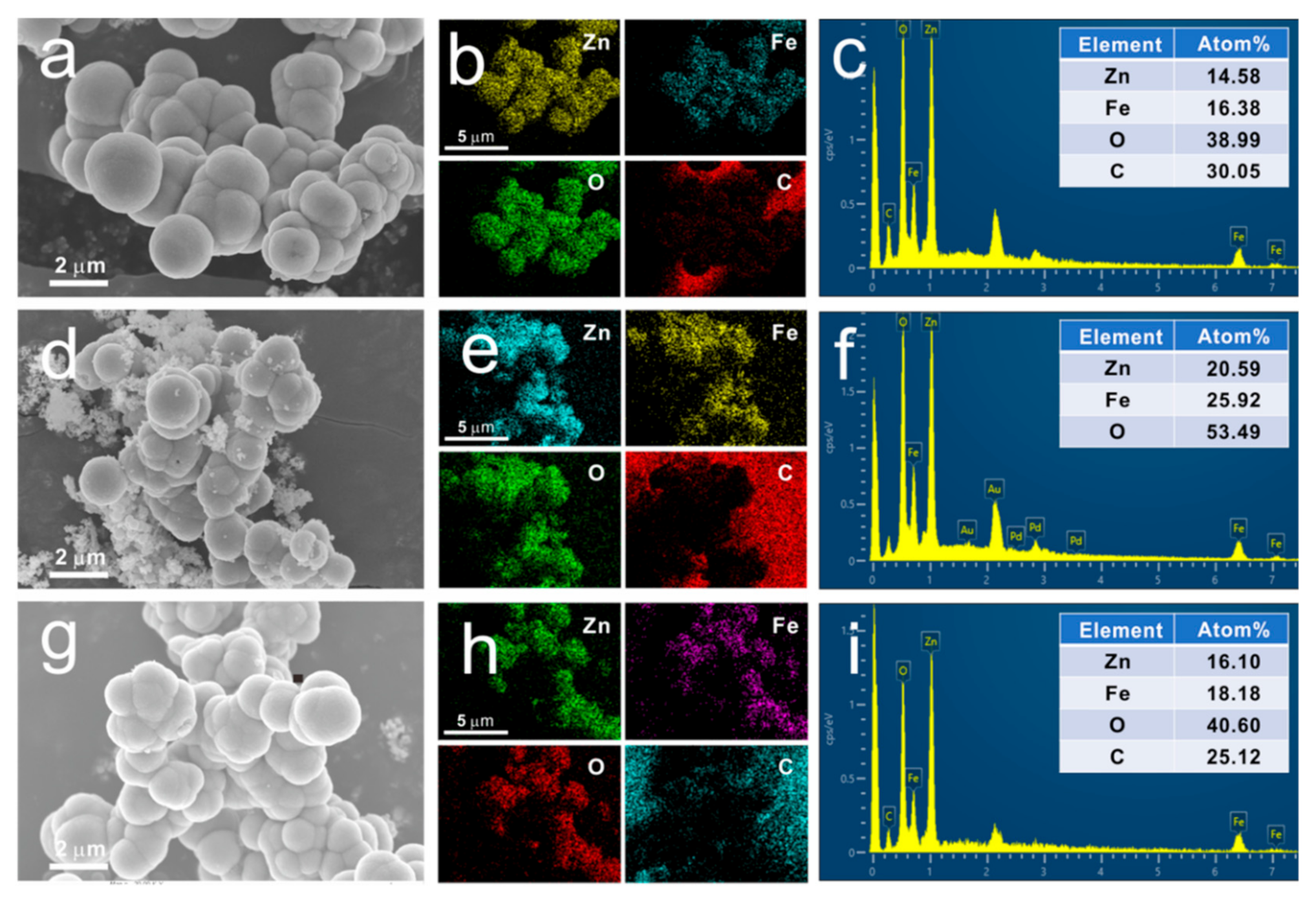
2.1. Synthesis of ZnFe2O4/ZnO/C Samples
2.2. Characterization
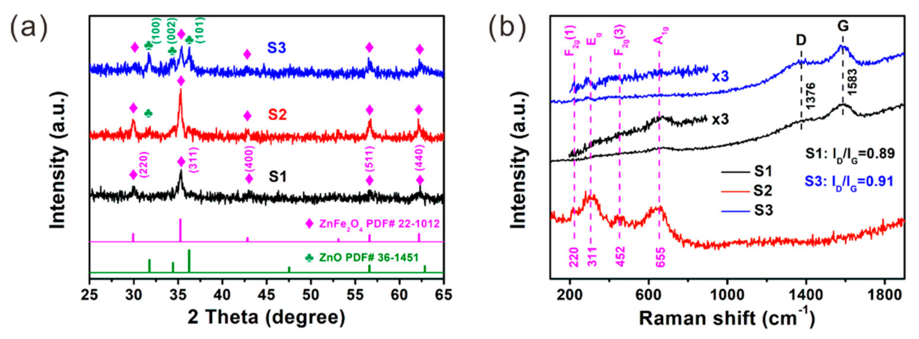
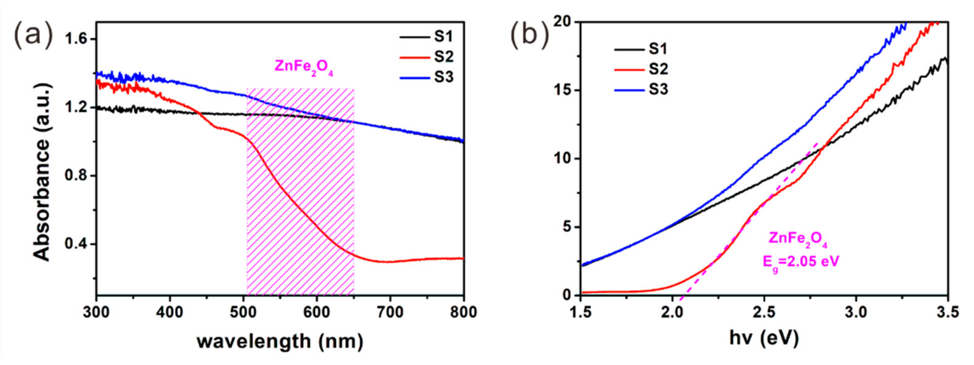
3. Results and Discussion
4. Conclusions
Supplementary Materials
Author Contributions
Funding
Institutional Review Board Statement
Informed Consent Statement
Data Availability Statement
Acknowledgments
Conflicts of Interest
References
- Younes, H.; Shoaib, N.; Rahman, M.M.; Abu Al-Rub, R.; Hong, H.; Christensen, G.; Chen, H.; Younes, A.B.; Al Ghaferi, A. Thin carbon nanostructure mat with high electromagnetic interference shielding performance. Synth. Met. 2019, 253, 48–56. [Google Scholar] [CrossRef]
- Cucurachi, S.; Tamis, W.L.; Vijver, M.G.; Peijnenburg, W.J.; Bolte, J.F.; de Snoo, G.R. A review of the ecological effects of radiofrequency electromagnetic fields (RF-EMF). Environ. Int. 2013, 51, 116–140. [Google Scholar] [CrossRef] [PubMed]
- Miller, A.B.; Sears, M.E.; Morgan, L.L.; Davis, D.L.; Hardell, L.; Oremus, M.; Soskolne, C.L. Risks to health and well-being from radio-frequency radiation emitted by cell phones and other wireless devices. Front. Public Health 2019, 7, 223. [Google Scholar] [CrossRef] [PubMed] [Green Version]
- Kim, J.H.; Lee, J.K.; Kim, H.G.; Kim, K.B.; Kim, H.R. Possible effects of radiofrequency electromagnetic field exposure on central nerve system. Biomol. Ther. 2019, 27, 265–275. [Google Scholar] [CrossRef]
- Moradi, M.; Naghdi, N.; Hemmati, H.; Asadi-Samani, M.; Bahmani, M. Effects of the effect of ultra high frequency mobile phone radiation on human health. Electron. Physician 2016, 8, 2452–2457. [Google Scholar] [CrossRef] [Green Version]
- Liu, J.L.; Zhang, L.M.; Wu, H.J. Anion-doping-induced vacancy engineering of cobalt sulfoselenide for boosting electromagnetic wave absorption. Adv. Funct. Mater. 2022, 32, 202200544. [Google Scholar] [CrossRef]
- Qin, M.; Zhang, L.; Zhao, X.; Wu, H. Defect induced polarization loss in multi-shelled spinel hollow spheres for electromagnetic wave absorption application. Adv. Sci. 2021, 8, 202004640. [Google Scholar] [CrossRef]
- Drmota, A.; Koselj, J.; Drofenik, M.; Žnidaršič, A. Electromagnetic wave absorption of polymeric nanocomposites based on ferrite with a spinel and hexagonal crystal structure. J. Magn. Magn. Mater. 2012, 324, 1225–1229. [Google Scholar] [CrossRef]
- Zeng, X.; Cheng, X.; Yu, R.; Stucky, G.D. Electromagnetic microwave absorption theory and recent achievements in microwave absorbers. Carbon 2020, 168, 606–623. [Google Scholar] [CrossRef]
- Su, X.; Han, M.; Wang, J.; Wu, Q.; Duan, H.; Liang, C.; Zhang, S.; Pu, Z.; Liu, Y. Regulated dielectric loss based on core-sheath carbon-carbon hierarchical nanofibers toward the high-performance microwave absorption. J. Colloid Interface Sci. 2022, 624, 619–628. [Google Scholar] [CrossRef]
- Sun, Q.; Zhang, X.; Liu, R.; Shen, S.; Wu, F.; Xie, A. Tuning the dielectric and microwaves absorption properties of N-doped carbon nanotubes by boron insertion. Nanomaterials 2021, 11, 1164. [Google Scholar] [CrossRef]
- Zhou, J.; Wei, B.; Wang, M.; Yao, Z.; Chen, P.; Zhou, C.; Li, Z. Three dimensional flower like ZnFe2O4 ferrite loaded graphene: Enhancing microwave absorption performance by constructing microcircuits. J. Alloys Compd. 2021, 889, 161734. [Google Scholar] [CrossRef]
- Zeng, X.; Jiang, G.; Zhu, L.; Wang, C.; Chen, M.; Yu, R. Fe3O4 nanoflower-carbon nanotube composites for microwave shielding. ACS Appl. Nano Mater. 2019, 2, 5475–5482. [Google Scholar] [CrossRef]
- Zhou, X.; Jia, Z.; Zhang, X.; Wang, B.; Liu, X.; Xu, B.; Bi, L.; Wu, G. Electromagnetic wave absorption performance of NiCo2X4 (X = O, S, Se, Te) spinel structures. Chem. Eng. J. 2021, 420, 129907. [Google Scholar] [CrossRef]
- Gao, N.; Li, W.-P.; Wang, W.-S.; Liu, D.-P.; Cui, Y.-M.; Guo, L.; Wang, G.-S. Balancing dielectric loss and magnetic loss in Fe–NiS2/NiS/PVDF composites toward strong microwave reflection loss. ACS Appl. Mater. Interfaces 2020, 12, 14416–14424. [Google Scholar] [CrossRef]
- Zhang, D.; Xiong, Y.; Cheng, J.; Chai, J.; Liu, T.; Ba, X.; Ullah, S.; Zheng, G.; Yan, M.; Cao, M. Synergetic dielectric loss and magnetic loss towards superior microwave absorption through hybridization of few-layer WS2 nanosheets with NiO nanoparticles. Sci. Bull. 2020, 65, 138–146. [Google Scholar] [CrossRef] [Green Version]
- Liu, J.; Jia, Z.; Zhou, W.; Liu, X.; Zhang, C.; Xu, B.; Wu, G. Self-assembled MoS2/magnetic ferrite CuFe2O4 nanocomposite for high-efficiency microwave absorption. Chem. Eng. J. 2022, 429, 132253. [Google Scholar] [CrossRef]
- Bao, W.; Chen, C.; Si, Z. An easy method of synthesis CoxOy@C composite with enhanced microwave absorption performance. Nanomaterials 2020, 10, 902. [Google Scholar] [CrossRef]
- Wang, Y.; Di, X.; Fu, Y.; Wu, X.; Cao, J. Facile synthesis of the three-dimensional flower-like ZnFe2O4@MoS2 composite with heterogeneous interfaces as a high-efficiency absorber. J. Colloid Interface Sci. 2021, 587, 561–573. [Google Scholar] [CrossRef]
- Lu, Z.; Wang, Y.; Di, X.; Cheng, R.; Yang, L.; Gao, P. Design of hierarchical core-shell ZnFe2O4@MnO2@RGO composite with heterogeneous interfaces for enhanced microwave absorption. Ceram. Int. 2022, 48, 5217–5228. [Google Scholar] [CrossRef]
- Li, F.; Zhuang, L.; Zhan, W.; Zhou, M.; Sui, G.; Zhou, A.; Bai, G.; Xiao, W.; Yang, X. Desirable microwave absorption performance of ZnFe2O4@ZnO@rGO nanocomposites based on controllable permittivity and permeability. Ceram. Int. 2020, 46, 21744–21751. [Google Scholar] [CrossRef]
- An, B.H.; Park, B.C.; Yassi, H.A.; Lee, J.S.; Park, J.-R.; Kim, Y.K.; Ryu, J.E.; Choi, D.S. Fabrication of graphene-magnetite multi-granule nanocluster composites for microwave absorption application. J. Compos. Mater. 2019, 53, 4097–4103. [Google Scholar] [CrossRef]
- An, B.H.; Park, B.C.; Kanagaraj, A.B.; Chaturvedi, P.; Yassi, H.A.; Park, J.-R.; Kim, Y.K.; Ryu, J.E.; Sanduleanu, M.; Choi, D.S. Microwave absorption properties of magnetite multi-granule nanocluster–multiwall carbon nanotube composites. Funct. Mater. Lett. 2019, 12, 19500115. [Google Scholar] [CrossRef]
- Younes, H.; Li, R.; Lee, S.-E.; Kim, Y.K.; Choi, D. Gradient 3D-printed honeycomb structure polymer coated with a composite consisting of Fe3O4 multi-granular nanoclusters and multi-walled carbon nanotubes for electromagnetic wave absorption. Synth. Met. 2021, 275, 116731. [Google Scholar] [CrossRef]
- Chai, L.; Wang, Y.; Zhou, N.; Du, Y.; Zeng, X.; Zhou, S.; He, Q.; Wu, G. In-situ growth of core-shell ZnFe2O4@ porous hollow carbon microspheres as an efficient microwave absorber. J. Colloid Interface Sci. 2021, 581, 475–484. [Google Scholar] [CrossRef]
- Gao, Z.; Xu, B.; Ma, M.; Feng, A.; Zhang, Y.; Liu, X.; Jia, Z.; Wu, G. Electrostatic self-assembly synthesis of ZnFe2O4 quantum dots (ZnFe2O4@C) and electromagnetic microwave absorption. Compos. Part B Eng. 2019, 179, 107417. [Google Scholar] [CrossRef]
- Li, H.; Hou, Y.; Li, L. Tunable design of yolk-shell ZnFe2O4@C composites for enhancing electromagnetic wave absorption. Powder Technol. 2021, 378, 216–226. [Google Scholar] [CrossRef]
- Shu, R.W.; Zhang, G.Y.; Wang, X.; Gao, X.; Wang, M.; Gan, Y.; Shi, J.J.; He, J. Fabrication of 3D net-like MWCNTs/ZnFe2O4 hybrid composites as high-performance electromagnetic wave absorbers. Chem. Eng. J. 2018, 337, 242–255. [Google Scholar] [CrossRef]
- Liao, Z.; Ma, M.; Tong, Z.; Wang, R.; Bi, Y.; Chen, Y.; Chung, K.L.; Ma, Y. Fabrication of ZnFe2O4/C@PPy composites with efficient electromagnetic wave absorption properties. J. Colloid Interface Sci. 2021, 602, 602–611. [Google Scholar] [CrossRef]
- Liu, Y.; Zhou, X.; Jia, Z.; Wu, H.; Wu, G. Oxygen vacancy-induced dielectric polarization prevails in the electromagnetic wave-absorbing mechanism for Mn-based MOFs-derived composites. Adv. Funct. Mater. 2022, 32, 2204499. [Google Scholar] [CrossRef]
- Tahir, A.A.; Wijayantha, K.G.U. Photoelectrochemical water splitting at nanostructured ZnFe2O4 electrodes. J. Photochem. Photobiol. A-Chem. 2010, 216, 119–125. [Google Scholar] [CrossRef]
- Qin, M.; Zhang, L.; Wu, H. Dual-template hydrothermal synthesis of multi-channel porous NiCo2O4 hollow spheres as high-performance electromagnetic wave absorber. Appl. Surf. Sci. 2020, 515, 146132. [Google Scholar] [CrossRef]
- Zhang, D.; Deng, Y.; Han, C.; Zhu, H.; Yan, C.; Zhang, H. Enhanced microwave absorption bandwidth in graphene-encapsulated iron nanoparticles with core–shell structure. Nanomaterials 2020, 10, 931. [Google Scholar] [CrossRef]
- Ahn, C.H.; Kim, Y.Y.; Kim, D.C.; Mohanta, S.K.; Cho, H.K. A comparative analysis of deep level emission in ZnO layers deposited by various methods. J. Appl. Phys. 2009, 105, 013502. [Google Scholar] [CrossRef]
- Galdamez-Martinez, A.; Santana, G.; Guell, F.; Martinez-Alanis, P.R.; Dutt, A. Photoluminescence of ZnO nanowires: A review. Nanomaterials 2020, 10, 857. [Google Scholar] [CrossRef] [PubMed]
- Vempati, S.; Mitra, J.; Dawson, P. One-step synthesis of ZnO nanosheets: A blue-white fluorophore. Nanoscale Res. Lett. 2012, 7, 470. [Google Scholar] [CrossRef] [Green Version]
- Cao, B.; Cai, W.; Zeng, H. Temperature-dependent shifts of three emission bands for ZnO nanoneedle arrays. Appl. Phys. Lett. 2006, 88, 161101. [Google Scholar] [CrossRef]
- Li, Q.; Fu, S.; Song, C.; Wang, G.; Zeng, F.; Pan, F. Sputtering power dependence of structure and photoluminescence of ZnO on 6H–SiC. J. Mater. Sci. Mater. Electron. 2017, 28, 17881–17888. [Google Scholar] [CrossRef]
- Granone, L.I.; Nikitin, K.; Emeline, A.; Dillert, R.; Bahnemann, D.W. Effect of the degree of inversion on the photoelectrochemical activity of spinel ZnFe2O4. Catalysts 2019, 9, 434. [Google Scholar] [CrossRef] [Green Version]
- Shen, H.; Shi, X.; Wang, Z.; Hou, Z.; Xu, C.; Duan, L.; Zhao, X.; Wu, H. Defects control and origins of blue and green emissions in sol-gel ZnO thin films. Vacuum 2022, 202, 111201. [Google Scholar] [CrossRef]
- Zhang, D.H.; Xue, Z.Y.; Wang, Q.P. The mechanisms of blue emission from ZnO films deposited on glass substrate by r.f. magnetron sputtering. J. Phys. D Appl. Phys. 2002, 35, 2837–2840. [Google Scholar] [CrossRef]
- Sundaram, K.B.; Khan, A. Work function determination of zinc oxide films. J. Vac. Sci. Technol. A Vac. Surf. Film. 1997, 15, 428–430. [Google Scholar] [CrossRef]
- Chen, G.; Zhang, L.; Luo, B.; Wu, H. Optimal control of the compositions, interfaces, and defects of hollow sulfide for electromagnetic wave absorption. J. Colloid Interface Sci. 2022, 607, 24–33. [Google Scholar] [CrossRef] [PubMed]
- Liao, Z.; Ma, M.; Tong, Z.; Bi, Y.; Chung, K.L.; Qiao, M.; Ma, Y.; Ma, A.; Wu, G.; Li, Z.; et al. Fabrication of one-dimensional ZnFe2O4@carbon@MoS2/FeS2 composites as electromagnetic wave absorber. J. Colloid Interface Sci. 2021, 600, 90–98. [Google Scholar] [CrossRef]
- Chen, P.; Zhang, N.; Chen, W.; Wang, Y. Rhombic Fe2O3 lumps doping hollow ZnFe2O4 spheres through oxidative decomposition process implanted into graphene conductive network with superior electromagnetic wave absorption properties. Ceram. Int. 2021, 47, 6453–6462. [Google Scholar] [CrossRef]
- Wu, H.; Lan, D.; Li, B.; Zhang, L.; Fu, Y.; Zhang, Y.; Xing, H. High-entropy alloy@air@Ni-NiO core-shell microspheres for electromagnetic absorption applications. Compos. Part B-Eng. 2019, 179, 107524. [Google Scholar] [CrossRef]
- Mei, Q.; Xiao, H.; Ding, G.; Liu, H.; Zhao, C.; Wang, R.; Huang, Z. Ultralight open-cell graphene aerogels with multiple, gradient microstructures for efficient microwave absorption. Nanomaterials 2022, 12, 1896. [Google Scholar] [CrossRef]
- Li, M.; Li, W.; Liu, S. Control of the morphology and chemical properties of carbon spheres prepared from glucose by a hydrothermal method. J. Mater. Res. 2012, 27, 1117–1123. [Google Scholar] [CrossRef]
- Liu, J.; Liang, H.; Wu, H. Hierarchical flower-like Fe3O4/MoS2 composites for selective broadband electromagnetic wave absorption performance. Compos. Part A-Appl. Sci. Manuf. 2020, 130, 105760. [Google Scholar] [CrossRef]
- Zhao, X.; Huang, Y.; Yan, J.; Liu, X.; Ding, L.; Zong, M.; Liu, P.; Li, T. Excellent electromagnetic wave absorption properties of the ternary composite ZnFe2O4@PANI-rGO optimized by introducing covalent bonds. Compos. Sci. Technol. 2021, 210, 108801. [Google Scholar] [CrossRef]
- Zhou, X.; Wen, J.; Wang, Z.; Ma, X.; Wu, H. Size-controllable porous flower-like NiCo2O4 fabricated via sodium tartrate assisted hydrothermal synthesis for lightweight electromagnetic absorber. J. Colloid Interface Sci. 2021, 602, 834–845. [Google Scholar] [CrossRef]
- Ding, D.; Wang, Y.; Li, X.; Qiang, R.; Xu, P.; Chu, W.; Han, X.; Du, Y. Rational design of core-shell Co@C microspheres for high-performance microwave absorption. Carbon 2017, 111, 722–732. [Google Scholar] [CrossRef]


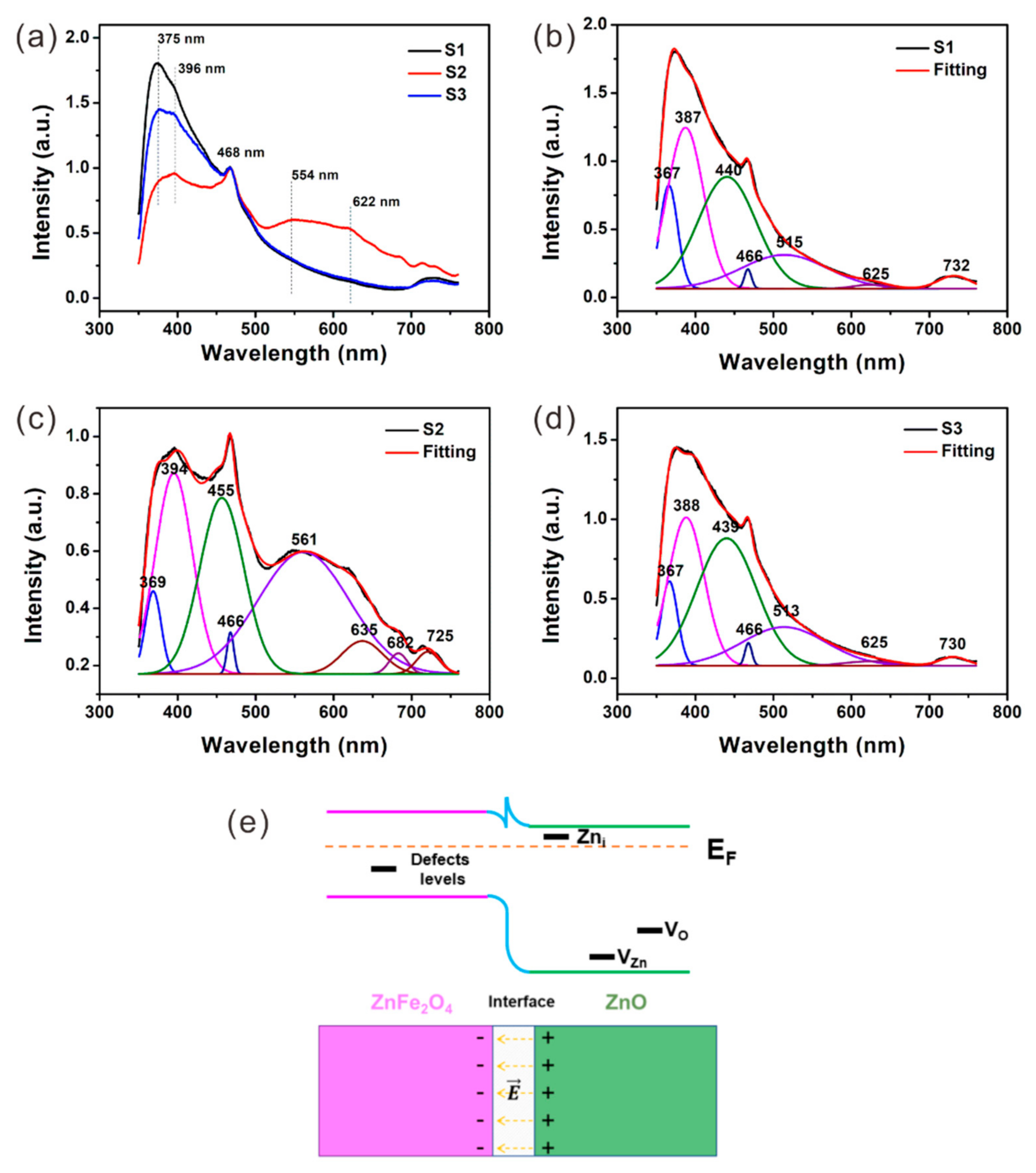
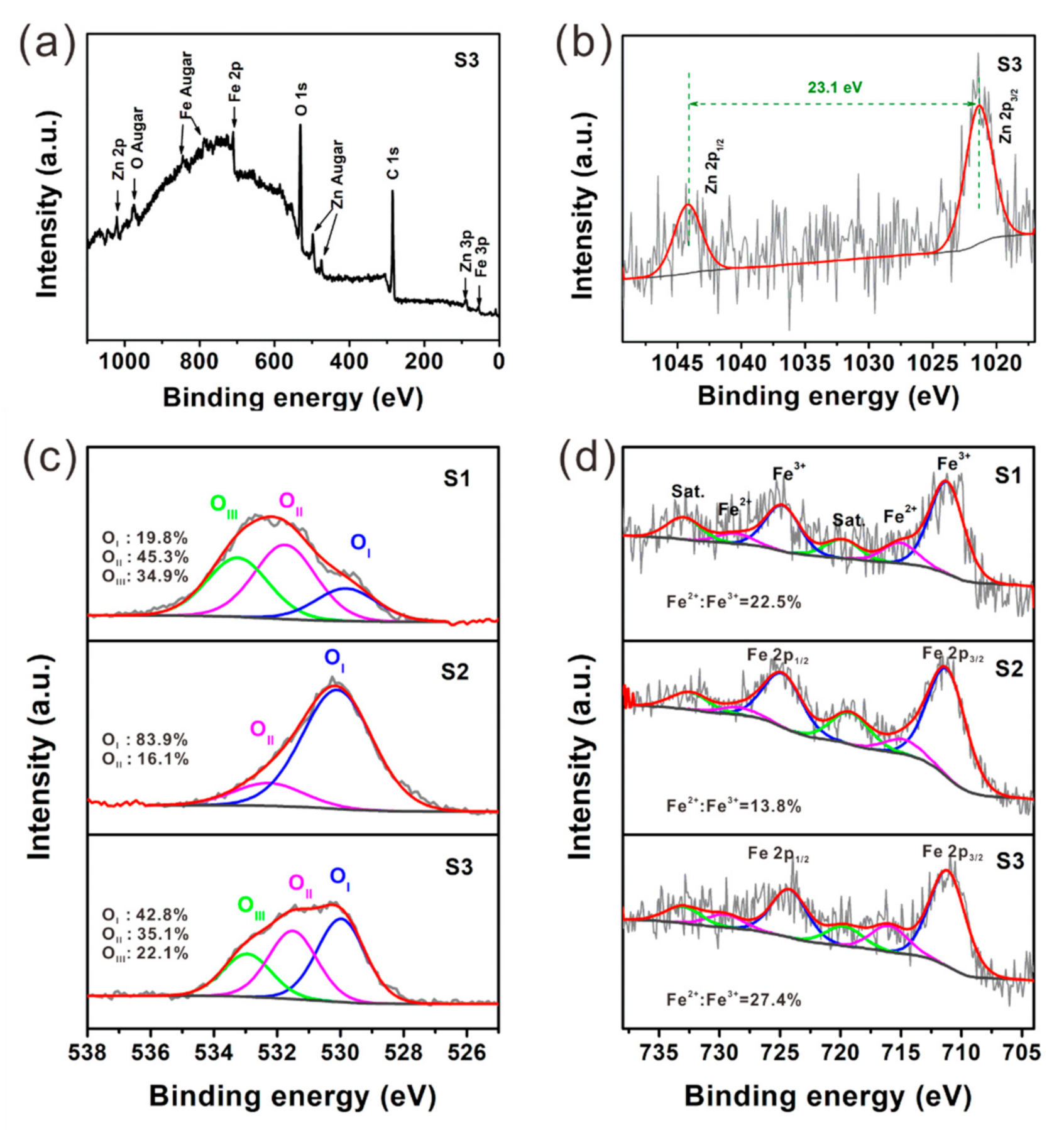
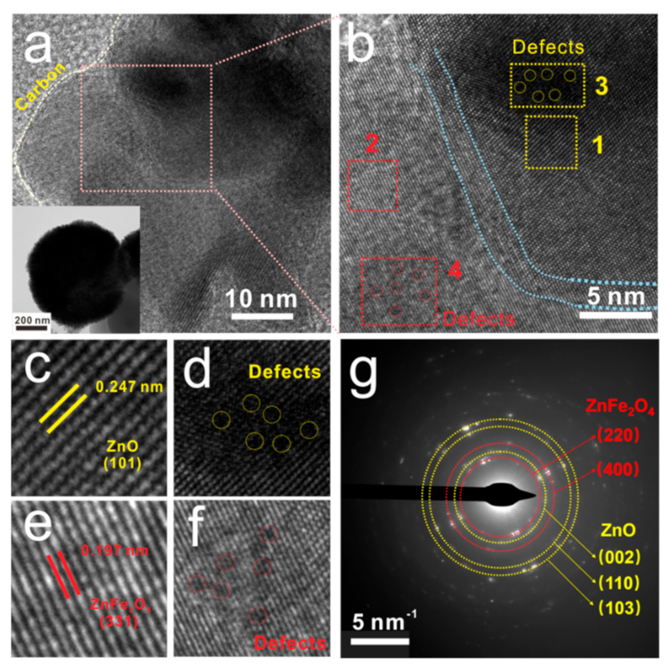
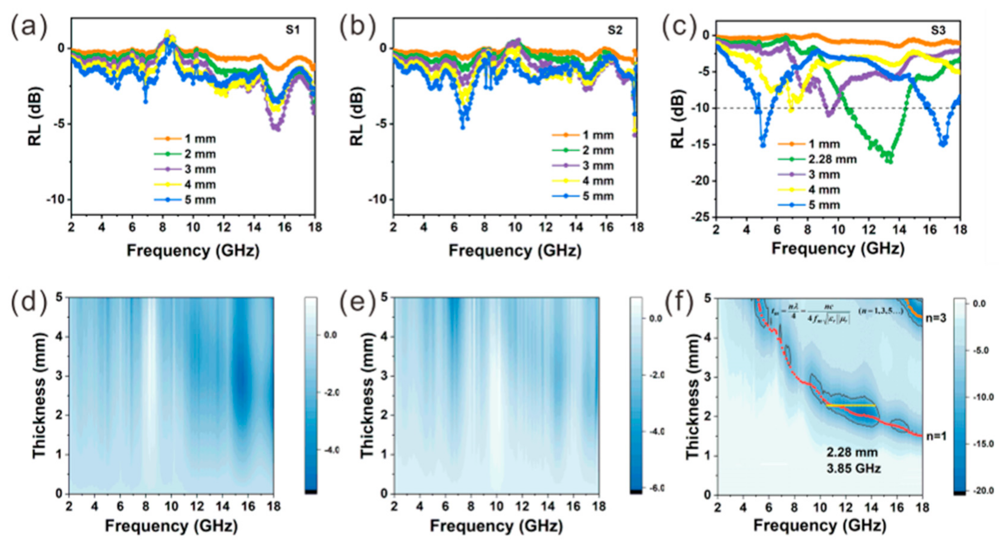
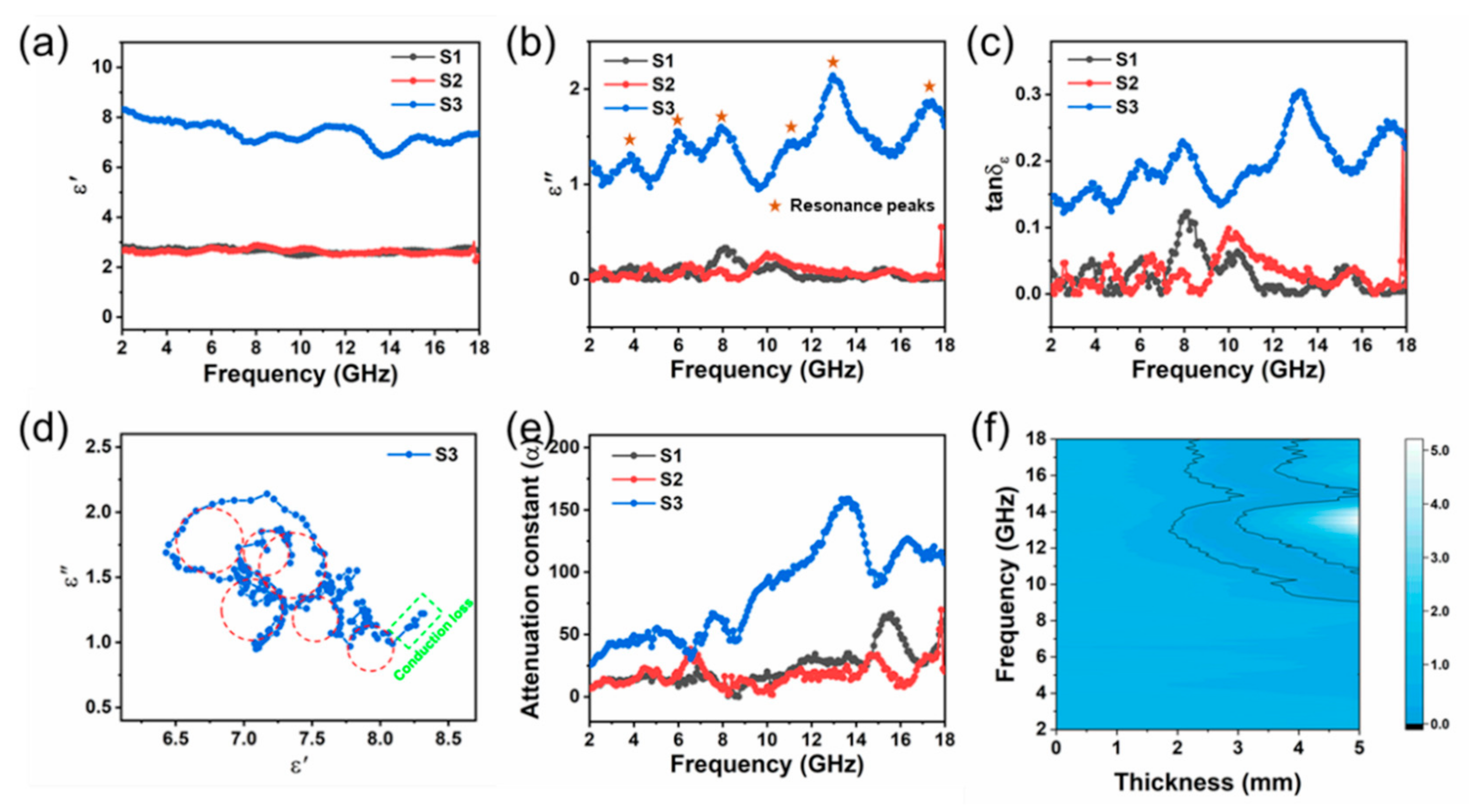
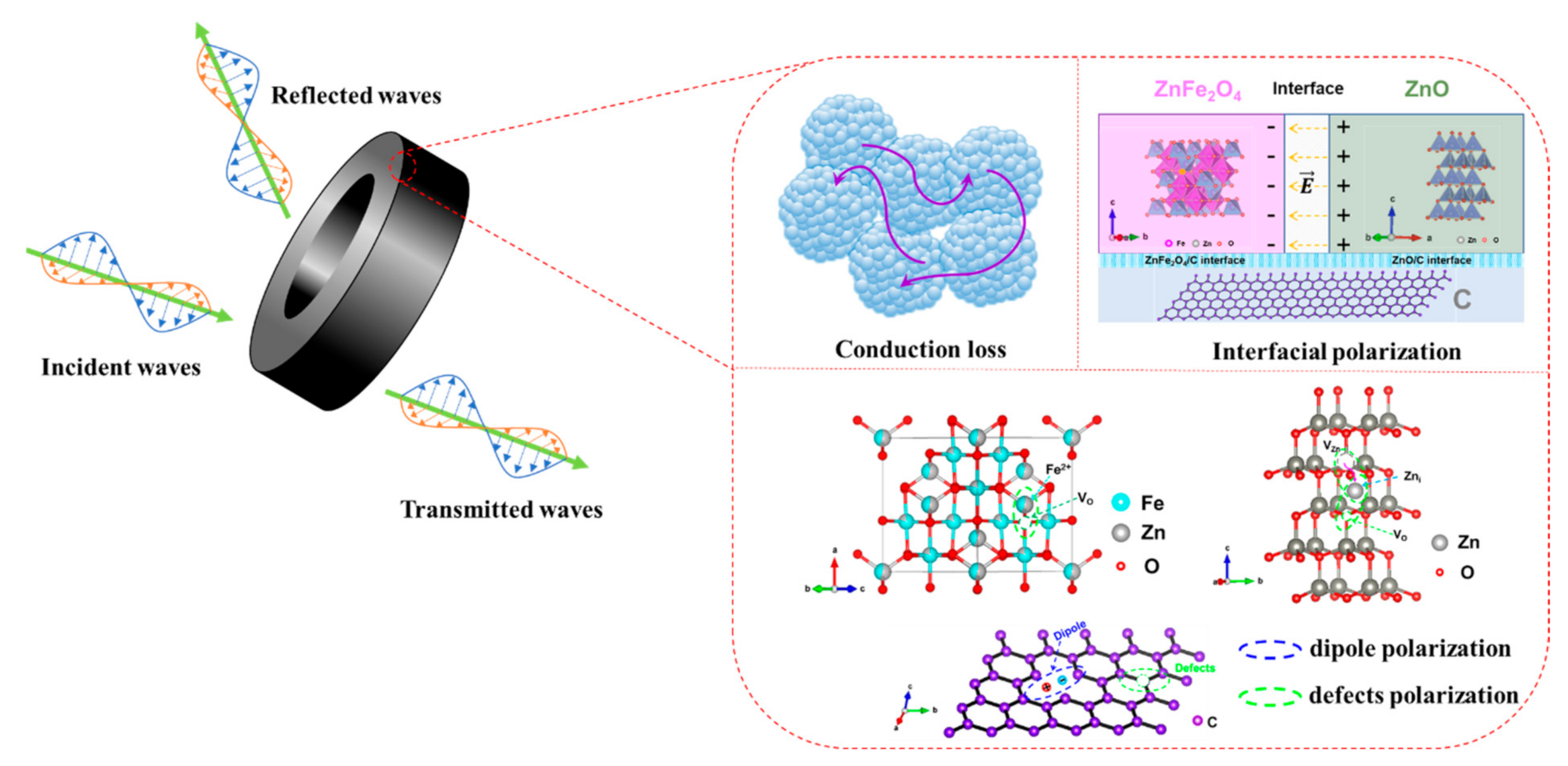
| Sample | Components & Interfaces | Defects | Permittivity | tan δε | RLmin & fe | ||||
|---|---|---|---|---|---|---|---|---|---|
| ZnFe2O4:ZnO:C | ID/IG | Zni&VZn | VO | Fe2+/Fe3+ | ε′ | ε″ | |||
| S1 | 1:0.78:3.67 | 0.89 | 0.89 | 45.30% | 22.50% | ~3.0 | ~0–~0.35 | ~0–~0.12 | −5.4 dB, - |
| S2 | 1:0.59:0 | - | 0.91 | 16.10% | 13.80% | ~3.0 | ~0–~0.30 | ~0–~0.10 | −5.2 dB, - |
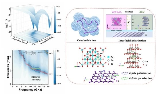
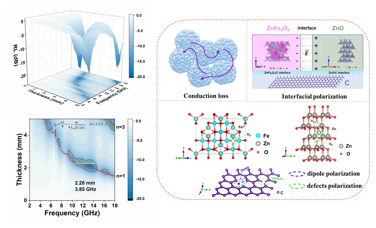
| S3 | 1:0.77:2.76 | 0.91 | 1.18 | 35.10% | 27.40% | ~6.8–~8.3 | ~1.0–~2.2 | ~0.12–~0.3 | −17.4 dB, 3.85 GHz |
Publisher’s Note: MDPI stays neutral with regard to jurisdictional claims in published maps and institutional affiliations. |
© 2022 by the authors. Licensee MDPI, Basel, Switzerland. This article is an open access article distributed under the terms and conditions of the Creative Commons Attribution (CC BY) license (https://creativecommons.org/licenses/by/4.0/).
Share and Cite
Shen, H.; Wang, Z.; Wang, C.; Zou, P.; Hou, Z.; Xu, C.; Wu, H. Defect- and Interface-Induced Dielectric Loss in ZnFe2O4/ZnO/C Electromagnetic Wave Absorber. Nanomaterials 2022, 12, 2871. https://doi.org/10.3390/nano12162871
Shen H, Wang Z, Wang C, Zou P, Hou Z, Xu C, Wu H. Defect- and Interface-Induced Dielectric Loss in ZnFe2O4/ZnO/C Electromagnetic Wave Absorber. Nanomaterials. 2022; 12(16):2871. https://doi.org/10.3390/nano12162871
Chicago/Turabian StyleShen, Hao, Zhen Wang, Chun Wang, Pengfei Zou, Zhaoyang Hou, Chunlong Xu, and Hongjing Wu. 2022. "Defect- and Interface-Induced Dielectric Loss in ZnFe2O4/ZnO/C Electromagnetic Wave Absorber" Nanomaterials 12, no. 16: 2871. https://doi.org/10.3390/nano12162871