Article

Exciton Luminescence and Optical Properties of Nanocrystalline Cubic Y2O3 Films Prepared by Reactive Magnetron Sputtering

1
Institute of Physics and Technology, Ural Federal University, 620075 Ekaterinburg, Russia
2
Institute of Metal Physics, Ural Branch of Russian Academy of Sciences, 620108 Ekaterinburg, Russia
3
Department of Industrial and Systems Engineering, The Hong Kong Polytechnic University, Hong Kong
4
Research Institute for Advanced Manufacturing, The Hong Kong Polytechnic University, Hong Kong
5
Institute of Electrophysics, Ural Branch of Russian Academy of Science, 620049 Ekaterinburg, Russia
*
Author to whom correspondence should be addressed.
Nanomaterials 2022, 12(15), 2726; https://doi.org/10.3390/nano12152726
Submission received: 28 June 2022 / Revised: 28 July 2022 / Accepted: 1 August 2022 / Published: 8 August 2022
(This article belongs to the Special Issue Low Dimensional Luminescent Nanomaterials and Nanodevices)

Abstract

:
This paper presents a comprehensive study of the energy structure, optical characteristics, and spectral-kinetic parameters of elementary excitations in a high-purity nanocrystalline cubic Y2O3 film synthesized by reactive magnetron sputtering. The optical transparency gaps for direct and indirect interband transitions were determined and discussed. The dispersion of the refractive index was established based on the analysis of interference effects. It was found that the refractive index of the Y2O3 film synthesized in this study is higher in order of magnitude than that of the films obtained with the help of other technologies. The intrinsic emission of Y2O3 film has been discussed and associated with the triplet–singlet radiative relaxation of self-trapped and bound excitons. We also studied the temperature behavior of the exciton luminescence of Y2O3 for the first time and determined thermal activation barriers. The optical energy and kinetic parameters of cubic Y2O3 films were analyzed in comparison with those of the monoclinic films of yttrium oxide. The main difference between the optical properties of cubic and monoclinic Y2O3 films was established, which allowed for a supposition of their application prospects.

1. Introduction

Thin film oxides play an important role in emerging technologies such as photonics; micro-, nano-, and opto-electronics; as well as alternative energy sources [1,2]. Rare-earth oxides represent a promising group of multifunctional materials since they exhibit significant optical properties which are useful for commercial employment: high dielectric constant (~12–16), optical transparency over a relatively wide spectral range, and low phonon energy (up to 600 cm−1) [3]. Additionally, rare-earth oxides can be successfully involved in the manufacturing of laser devices, optical fibers, light-emitting diodes, high-frequency diodes, etc. [4]. One of the actively studied materials in this category is yttrium oxide (Y2O3), which is considered as a suitable host matrix for ionic dopants (including rare-earth and transition-metal ions) in order to construct and develop solid-state optical devices [5,6,7].
Three structural Y2O3 polymorphs are currently known: cubic, monoclinic, and hexagonal, which are commonly referred to as C-, B-, and A-type structures, respectively [8]. Among these crystal structures, cubic Y2O3 is the most stable phase under normal conditions (room temperature and atmospheric pressure). The optical properties of a cubic Y2O3 host in various modifications (bulk crystal, transparent ceramic, nanoparticles) have recently been studied in sufficient detail (e.g., see Refs. [9,10,11,12]). It has been found for bulk crystalline Y2O3 that the intrinsic luminescence of such a host matrix is associated with excitons and optically active defects. Additional interesting results concerning the interactions between excitons and ionic dopants have been reported as well. The energy transfer from self-trapped excitons to rare-earth ions in Y2O3 nanoparticles was discovered, and the quenching model of intrinsic luminescence in Y2O3 was proposed in Refs. [12,13]. As for the film-based morphology of yttrium oxide, data concerning the energy gap and the refractive index of Y2O3 were reported in Refs. [14,15] for radio frequency magnetron sputtering synthesis technology, electron beam deposition [16], thermal evaporation [17], and atomic vapor deposition techniques [18]. At the same time, the systematic studies on the emission properties of Y2O3 films are almost non-existent. It is for this reason that this is still one of the most challenging problems in this area of research since the information about the complex properties of the Y2O3 host matrix is highly essential for the onward development of functional materials for commercial applications.
The purpose of the current study is to discover the optical properties of Y2O3 thin films synthesized by reactive magnetron sputtering. We aimed to accomplish the following research tasks: to obtain high-purity films with low defectiveness; to study their energy structure and fundamental optical characteristics, including the spectral-kinetic parameters of elementary excitations; to compare our Y2O3 data with similar films synthesized by other technologies; and finally, to establish the influence of structural factors on the optical, energy, and kinetic parameters of nanocrystalline Y2O3 films. The data obtained will provide the necessary groundwork for the onward development of thin-film Y2O3 materials.

2. Materials and Methods

Y2O3 film was deposited onto a silica glass substrate using the dc-pulsed mode (50 kHz, 10 μs) of the reactive magnetron sputtering technology. Before the deposition process, the silica glass substrate was cleaned in an acetone solvent using an ultrasonic bath for 20 min, followed by drying in air. A target with a 40 mm diameter and a 2 mm thickness was yielded by employing the cold pressing procedure on metallic yttrium powder at 30 MPa. The magnetron, the sputtered target, and the substrate were placed in a vacuum chamber pumped down to 6.6 × 10⁻³ Pa with the help of a turbomolecular pump. Sputtering was carried out at 30 W magnetron power for 8 h, in an argon–oxygen atmosphere with a total pressure of 0.4 Pa and an oxygen volume concentration of less than 30%. The temperature of the substrate was maintained at 400 ± 25 °C during the deposition procedure. After deposition, the sample was cooled down to room temperature in a vacuum chamber with a pressure of 10–5 Torr. The thickness of the Y2O3 film was estimated to be at ~800 nm; it was determined by employing the ball-abrasion method with the help of the Calotest device (CSM Instruments SA, Peseux, Switzerland).
The structural-phase analysis of the sample under study was performed by means of an X-ray diffraction technique using the XPertPro MPD diffractometer with Cu Kα = 1.5405 Å radiation. The processing of diffraction patterns was performed using the TOPAS 3 full-profile analysis program, taking into account the presence of a predominant orientation of crystallites (texture) in the material under the study. The diffraction pattern shown in Figure 1 can be identified based on one crystalline phase—the cubic Y2O3 (Ia-3 space group) with a lattice parameter of a = 10.73 Å. Plane (111), which is parallel to the surface, was found to be the preferred orientation. The wide diffused peak observed in the pattern is due to the silica glass substrate. No diffraction and reflection associated with the monoclinic modification of Y2O3 were found. The average size of 10 nm for the coherent scattering D was obtained from the Scherrer equation D = k λ β cos θ , where λ is the wavelength of the X-ray, k is a constant equal to 0.89, θ denotes the Bragg angle, and β is the half-width of the line profile [19]. The average microstrain ε of the film was found to be 7.4 × 10⁻³ as ε = β cot θ 4 [20]. In the Scherrer method used, the crystallite size and the magnitude of the microstrain were determined separately from the same (222) peak without considering the instrumental broadening. In this case, the obtained values of D and ε are the lower bound on the crystallite size and the upper bound on the microstrain, respectively. The theoretical density of the film was determined to be at 4.86 g/cm3 using the equation ρ = Z M w NV [21], where Z is the number of formula units per unit cell, M w is the molecular weight, V denotes the volume of unit cell, and N is Avogadro’s number.
A chemical purity inspection of the sample under study was carried out using a ThermoScientific K-alpha Plus XPS spectrometer, which was equipped with a monochromatic micro-focused Al Kα X-ray source and had 0.05 at.% element sensitivity [22]. Operating pressure in an analytic chamber during a fast-wide scan (survey spectroscopy, 200 eV pass energy mode of a 180° hemispherical energy analyzer) was higher than 3.2 × 10⁻⁶ Pa. A dual-channel automatic charge compensator was applied to exclude the charging of our sample under XPS analysis because of the loss of photoelectrons. We performed pre-run-up procedures, including the standard degassing of the sample and analyzer, binding energy scale inspection, and re-calibration (when needed). In addition, we employed sputter-cleaned Au (4f7/2 band), Ag (3d5/2 band), and Cu (2p3/2 band) with built-in XPS Reference Standards according to the ISO 16.243 XPS International Standard and the XPS ASTM E2108-00 Standard. We used the built-in electronic database of ThermoScientific XPS spectrometer (ThermoFisher Scientific Waltham, Massachusetts, USA), the NIST XPS Standard Reference Database [23], and the Handbook of Monochromatic XPS Spectra: The Elements of Native Oxides [24] to precisely identify the survey spectrum structure (see Figure 2).
As can be seen in Figure 2, the most intensive peaks belong to yttrium and oxygen, which are the components of yttrium oxide. Carbon contamination (3.97 at.%) exists in the survey spectrum of the inspected Y2O3 sample, which is due to the well-known ability of Y2O3 to absorb CO and CO2 spices from the atmosphere (e.g., see Ref. [25]) and the general comments of ThermoScientific on the XPS study of yttrium oxide [26]. The measured O/Y ratio gives the value of 1.50, which is very close to the O/Y ratio = 1.51 of cubic Y2O3 [25]. The obtained value is dissimilar to the O/Y ratio = 1.46 of monoclinic Y2O3 reported in Ref. [27]. The XPS analysis of the survey spectrum confirms the formation of cubic high-purity Y2O3 film.

3. Results and Discussion

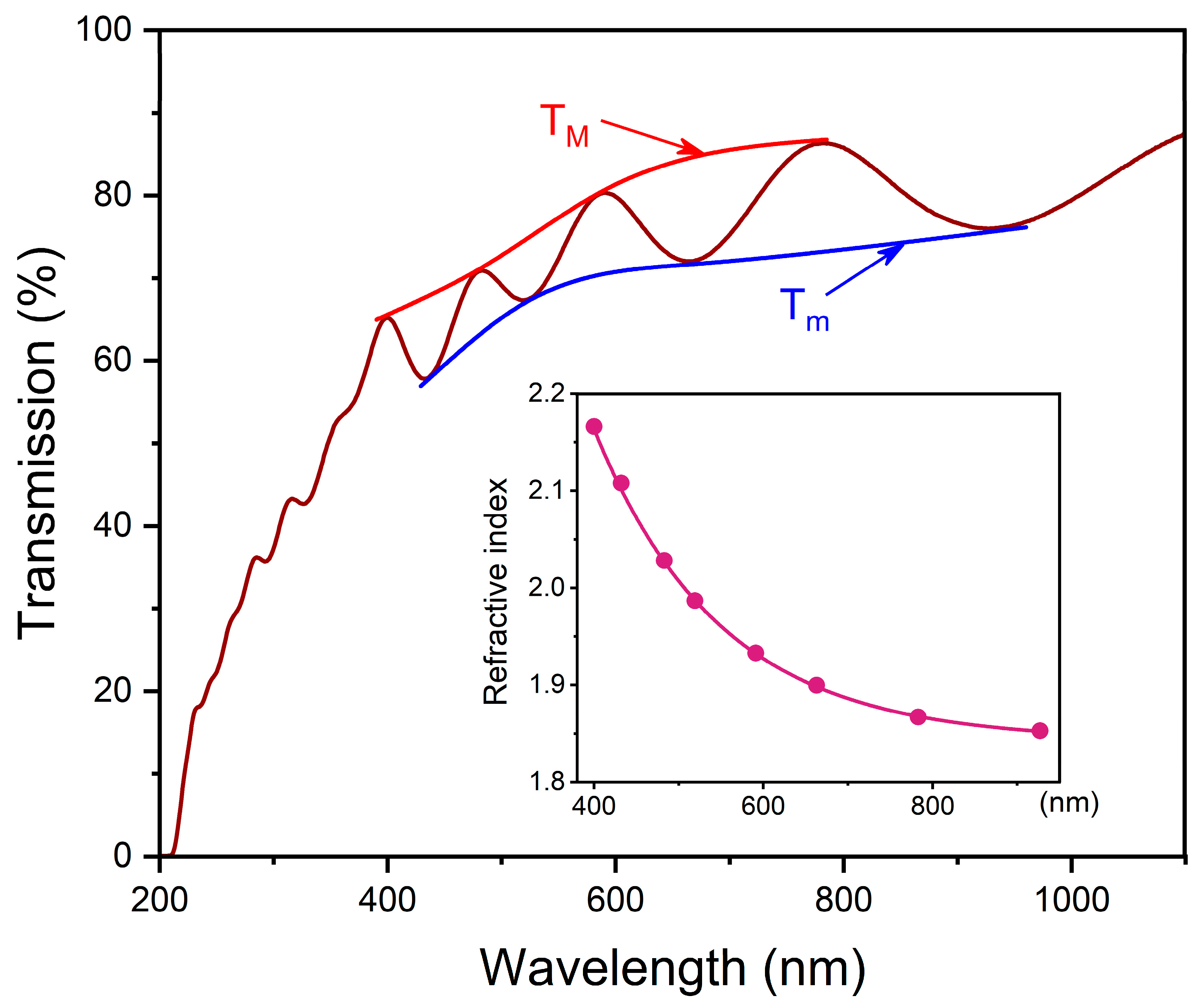
3.1. Interference and Refractive Index

Figure 3 shows the optical transmission spectrum of Y2O3 film. The well-discernible interference extremes observed in the range of the optically transparent film indicate the high uniformity of the film and the clear-cut boundary between the film and the substrate. In order to determine the spectral dependence of the refractive index, we employed Swanepoel’s method [28] based on the analysis of interference effects. This method allowed for the construction of the upper T M and lower T m envelopes of the spectrum, which are shown in Figure 3 by the red and blue lines, respectively.
The values of the upper and lower “envelopes” are substituted in order to perform calculations of the refractive index n ( λ ) :
n ( λ ) = N ( λ ) + N ( λ ) 2 n s 2
N ( λ ) = 2 n s T M ( λ ) T m ( λ ) T M ( λ ) T m ( λ ) + n s 2 + 1 2
where N ( λ ) is the calculated intermediate value; n s denotes the refractive index of the substrate ( n s = 1.452 1.469 for silica glass in the studied spectral range); T M ( λ ) and T m ( λ ) are the upper and lower “envelopes” of the optical transmission spectrum, respectively. The measured refractive index for the wavelengths corresponds to interference extrema and is represented by the circles in the inset of Figure 3. Spectral dependence n ( λ ) can be described using the simplified Cauchy equation (see violet line in the inset of Figure 3) [29]:
n ( λ ) = n 0 + A λ 2
where A = 6.1 × 10 4   ± 0.1 × 10 4 is a constant and n 0 = 1.783 ± 0.005 denotes the refractive index when λ . The mean of refractive index dispersion is D = n F n C = 0.117 ± 0.005 where n F and n C are the refractive indexes at 486.1 nm and 656.3 nm, respectively.
In the targeted range of the spectrum, magnetron-sputtered cubic Y2O3 film produces a higher refractive index when compared with that for Y2O3 films synthesized with the use of other methods. For example, the refractive indices of cubic Y2O3 films synthesized by means of radio frequency magnetron sputtering [15], electron beam deposition [16], and thermal evaporation [17] in the range of 400–800 nm are n = 1.95 1.91 , n = 1.93 1.89 , and n = 1.82 1.72 , respectively. In addition, the Y2O3 film inspected in our study exhibits a relatively high dispersion of the refractive index, which is larger in order of magnitude than that reported in the literature for other Y2O3 films. It is known that refractive index is related to the porosity and packing density of a material [30]. One can estimate the porosity (P) and packing density ( P d = 1 P ) of the film using the known Lorentz–Lorenz expression [31]:
n 2 1 n 2 + 1 = n b 2 1 n b 2 + 2 ( 1 P )
where n and n b denote the refractive index of the film and the bulk material, respectively. Assuming that the refractive index value of bulk yttria is n b = 1.937 at 590 nm [32], and accounting for experimental data obtained for the film, the porosity of the film was estimated to be P = 0.003 . The obtained value is smaller in order of magnitude than the value determined for films prepared by the electron beam deposition technique [16]. We believe that the increased refractive index value of our film is due to its high packing density.
Based on the spectral dependence of the refractive index, the thickness of Y2O3 film can be determined as follows:
d = λ 1 λ 2 2 ( λ 2 n 1 λ 1 n 2 )
where n 1 and n 2 are refractive indices at wavelengths λ 1 and λ 2 , which correspond to the maxima (minima) of the neighboring interference observed in the transmission spectrum. Using several pairs of interference extrema, the average thickness of Y2O3 film is 812 ± 5 nm. The film thickness value obtained analytically is close to that declared during the synthesis stage (800 nm—ball-abrasion method). In the next stage of our research, we pay attention to the optical absorption of Y2O3 film.

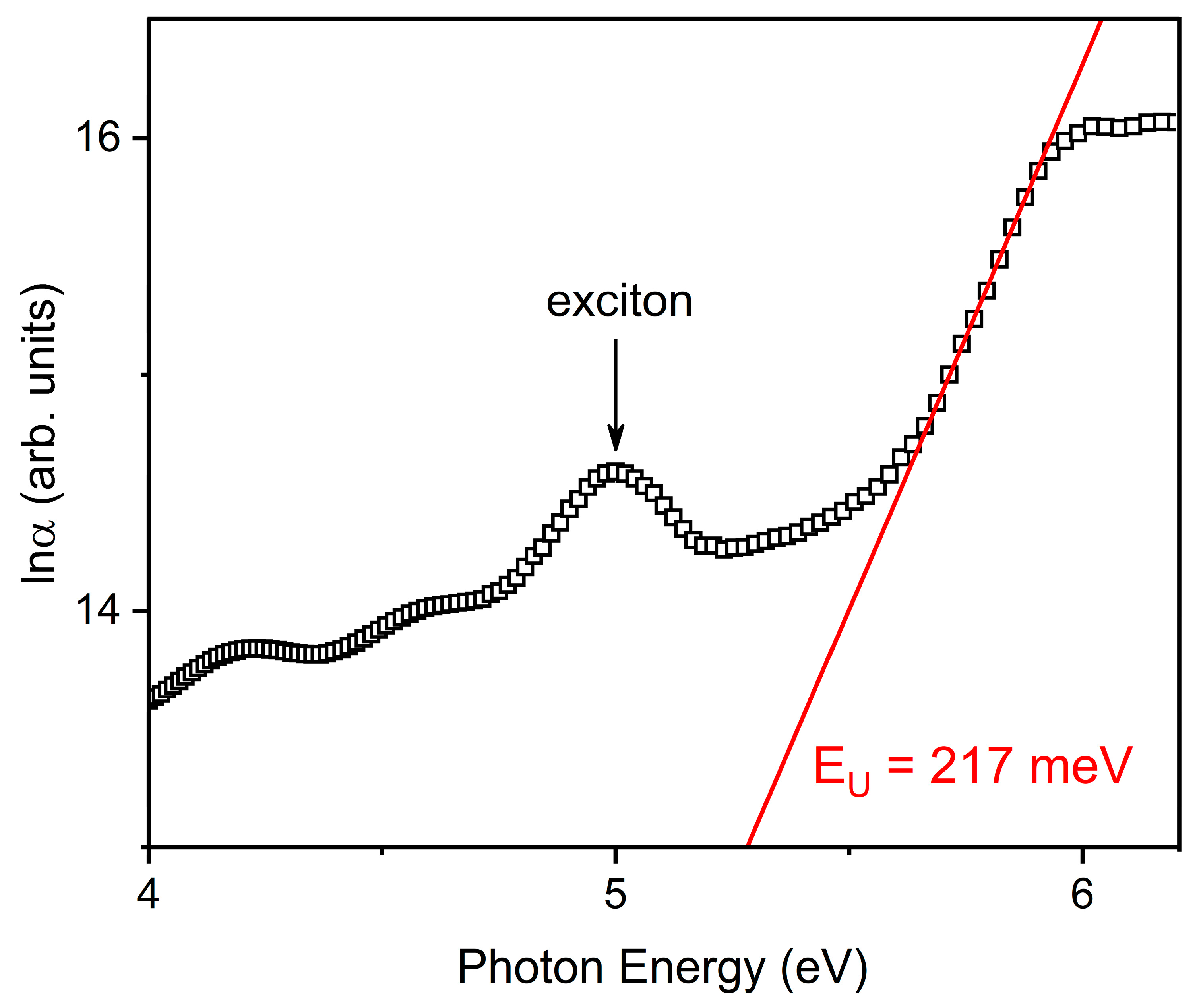
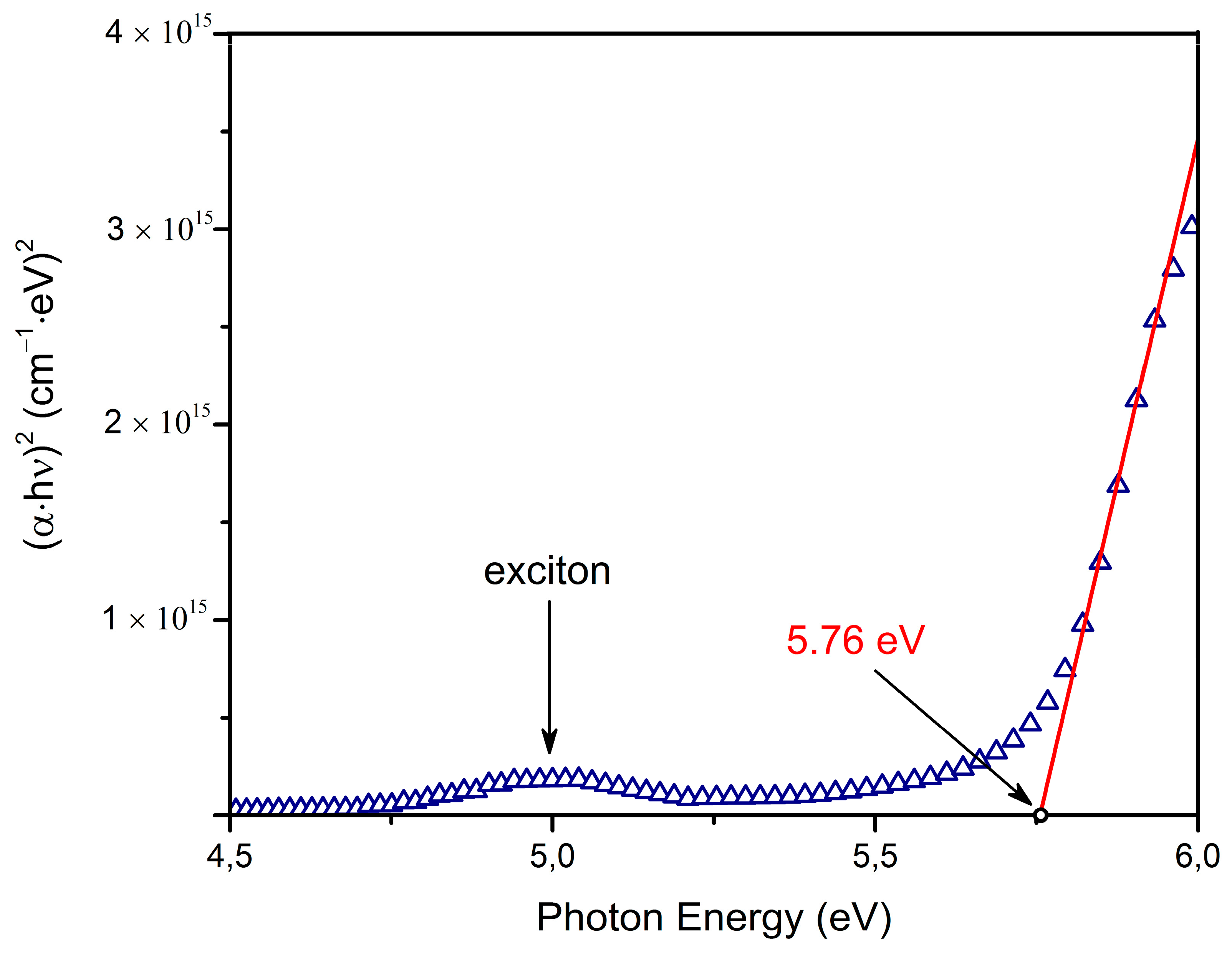
3.2. Energy Gaps and Interband Transitions

Figure 4 shows the spectral dependence of the absorption coefficient in the tails of the region of the density of states, which was analyzed using the following expression for the Urbach rule [33]:
α ( h v ) = α 0 exp ( h ν E 0 E U )
where α 0 is a constant, E 0 denotes the coordinate of the crossing point of the so-called “crystal-like” Urbach rule, and E U is the Urbach energy denoting the measure of the overall structural disorder of the system under study (static and dynamic) [34]. The Urbach absorption edge is formed by optical transitions between the localized electronic states. The E U is a measure of the overall disorder of the material in our study. Based on the principle of equivalence and additivity of static (“frozen” phonons) and dynamic (“thermal” phonons) disorders, the Urbach energy reflects both the intrinsic irregularities of the lattice (i.e., defects, impurities, deviations from stoichiometry, etc.) and the thermal effects induced by the electron–phonon interaction [35,36].
The inverse slope of the linear range of ln α ( h ν ) dependence refers to E U = 217 ± 2 meV (Figure 4). We have to note that the exact value of the Urbach energy was unknown for Y2O3. We compared the obtained E U value with that of other materials in the same family of rare-earth oxides–cubic gadolinium oxide films [37]. In our recent study, the Urbach energy of the Gd2O3 film was 483 ± 2 meV, and the intrinsic defects had significantly higher concentrations, which ensured a higher degree of structural disorder. As for the Y2O3 film, the Urbach energy was smaller, which indicates a relatively lower degree of total structural atomic disorder. In this case, a comparison of the Urbach energy for the Gd2O3 and Y2O3 films at room temperature gave a relatively good estimation of the total structural disorder, which is a combination of static and dynamic (phonon) disorders.
The analysis of the fundamental absorption edge was performed with the help of the Tauc equation [38,39]:
( α h v ) n = A ( h v E g )
where A is a constant; α denotes the absorption coefficient; h v is the photon energy; E g denotes the optical transparency gap, and n is the exponent which depends on the type of transitions. We studied direct allowed transitions at n = 2. The corresponding energy gap was determined by extrapolating the linear range of the ( α h v ) 2 function to the intersection with the abscissa axis, as shown in Figure 5. On the one hand, the measured optical transparency gap is 5.76 eV, which is very close to the value of the optical transparency gap for the Y2O3 film synthesized by means of radio frequency magnetron sputtering ( E g = 5.79 eV) [14]. On the other hand, the optical transparency gap of our sample is slightly larger than that for the Y2O3 film synthesized by employing atomic vapor deposition ( E g = 5.60 eV) [18].
A band with its maximum at 5.0 eV was found in the absorption spectra (see Figure 4 and Figure 5). We believe that the origin of this band is associated with exciton absorption. It is known that for the bulk cubic Y2O3, a self-trapped exciton is formed by means of photon absorption and with an energy level of 6.0 eV [9]. As for Y2O3 nanoparticles with an average size of 10 nm, the exciton absorption band exhibits at 5.9 eV [40]. However, there are no data concerning the optical properties of excitons in Y2O3 thin films. The exciton absorption band of Y2O3 film is shifted to a low-energy region if compared with bulk materials and nanoparticles. The luminescent properties of excitons in Y2O3 film will later be studied in more detail.

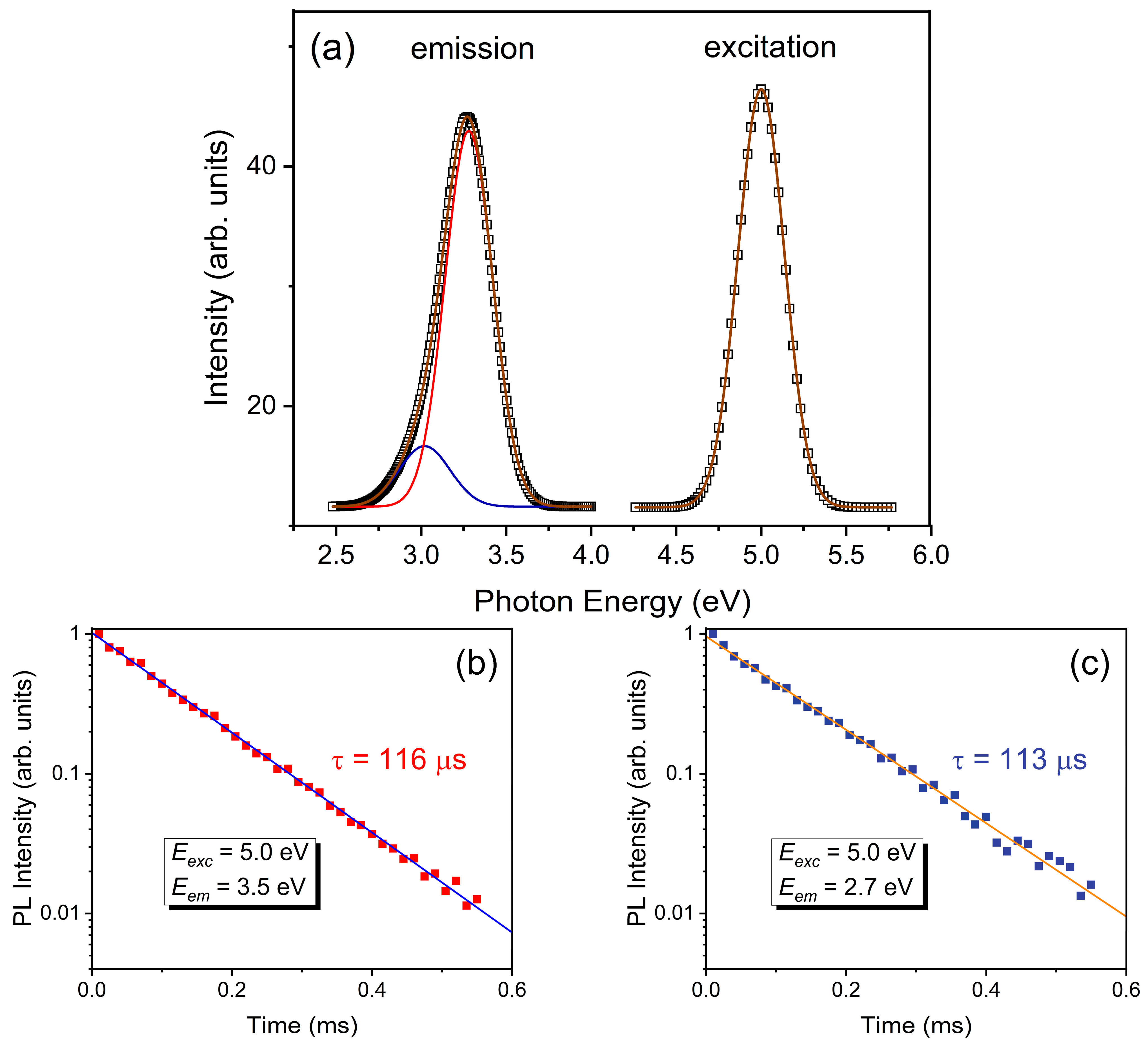
3.3. Room-Temperature Exciton Emission

Figure 6a shows the emission spectrum of the Y2O3 film under an excitation energy of 5.0 eV at room temperature. This emission spectrum is represented by the superposition of two bands whose maxima are located at 3.3 eV (FWHM = 0.3 eV) and 3.0 eV (FWHM = 0.3 eV). The excitation spectra of these two emission bands are similar to each other, and they produce one band with its maximum at 5.0 eV (FWHM = 0.3 eV). The locations of the excitation spectra were carefully calibrated. Otherwise, an overlapping of the spectra might have occurred.
For cubic Y2O3 in different morphologies (bulk crystal, transparent ceramic, nanoparticles), the luminescence at 3.4–3.5 eV is related to the radiative de-excitation of self-trapped excitons (STE) [9,11,12,41,42]. We believe that the dominant emission band located at 3.3 eV is also associated with the STE radiative recombination in Y2O3 film, and the spectral position of this band is shifted to the low-energy region when compared to bulk and low-dimensional cases. As for the second emission band, it is located at 3.0 eV, and the low-intensity luminescent band observed in the cubic Y2O3 is associated with the radiative recombination of the bounded exciton (BE), which was localized in the anion vacancy center of the F-type [11,42]. Thus, we believe that emission bands located at 3.3 eV and 3.0 eV are associated with STE and BE, respectively.
Figure 6b,c show the decay curves of exciton emission. The measurements were carried out by monitoring the emission wavelengths at the tails of the bands in order to avoid their overlap. The decay curves of both emission bands are single-exponential, and the emission lifetimes are 116 μs (Eem = 3.5 eV) and 113 μs (Eem = 2.7 eV). A large Stokes shift and slow luminescence decay kinetics indicate that the observed luminescence bands are associated with triplet–singlet radiative transitions. Triplet emission is usually characterized by a flare-up process because it overcomes the thermal activation barrier of the intersystem crossing (ISC) from a high-energy singlet state (S1) to a low-energy triplet state (T1) [43,44]. In the next section, we discuss our study of the temperature behavior of exciton-related emission.

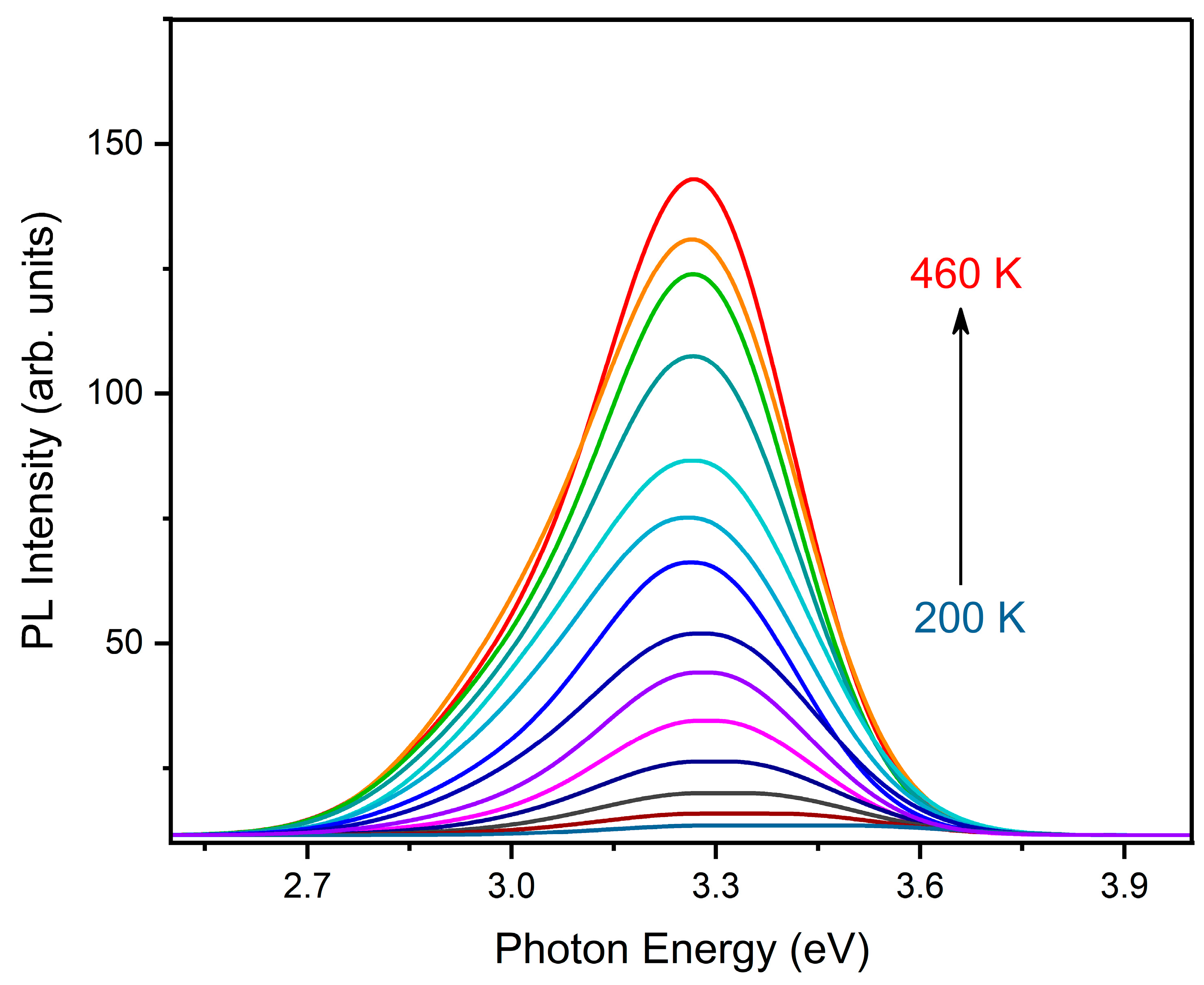
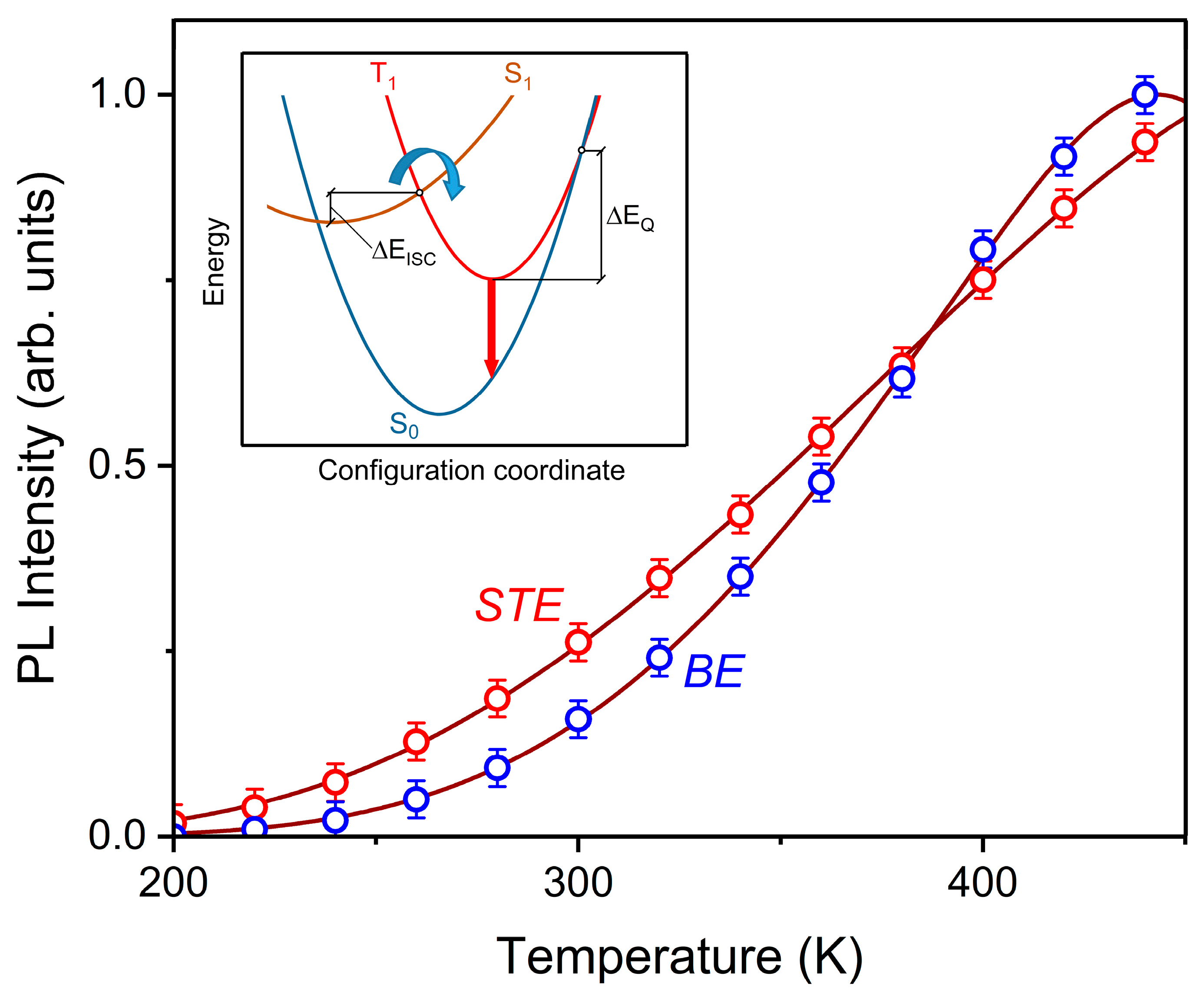
3.4. Temperature Behavior of Exciton Emission: Activation Barriers

The temperature-dependent emission spectra of Y2O3 film excited by 5.0 eV are shown in Figure 7. It can be seen that emission appears at ~200 K, where its intensity increases with temperature growth. The maxima of bands have no significant changes in their energy locations and FWHMs. It can be seen that the temperature broadening of emission bands is absent, and this indicates a relatively weak exciton–phonon interaction. As a consequence, it produces a high-efficiency radiative relaxation. No new luminescence bands were found at low temperatures, which can be associated with singlet–singlet radiative transitions. This phenomenon probably occurs due to the small thermal activation barrier of the singlet–singlet non-radiative transition. Normalized temperature dependences of integrated intensities of luminescence bands whose maxima are located at 3.2 eV (STE) and 3.0 eV (BE) are shown in Figure 8. It can be noted that BE-related emission flares up at high temperatures and quenches at low temperatures. Hence, the thermal activation barriers of flare-up emission and luminescence quenching for STE and BE are certainly different.
In order to determine thermal activation barriers, we analyzed the temperature dependences of emission using the following analytical expression, which takes into account flare-up emission and luminescence quenching [43]:
I ( T ) = I 0 { 1 + C 1 exp ( E I S C k T ) } { 1 + C 2 exp ( E Q k T ) }
where I 0 is the maximum luminescence intensity if the quantum effects yield ISC and radiative recombination is equal to 1; C 1 and C 2 are kinetic factors of ISC and the triplet radiative transition, respectively; E I S C is the thermal activation barrier of ISC; E Q denotes the thermal activation barrier of emission quenching. Our experimental data are shown in Figure 8. The values of E I S C and E Q during STE emission are 131 meV and 482 meV, respectively. In contrast, the values of E I S C and E Q during BE emission are 189 meV and 412 meV, respectively (an accuracy of ±2 meV).
The BE emission is characterized by a larger flare-up barrier and a lower quench barrier when compared with the STE emission. The differences between these two thermal activation barriers are related to the non-identical adiabatic potential curves of STE and BE. A configuration coordinate diagram is shown in the inset of Figure 8. Symbols S0, S1, and T1 denote the singlet ground state, singlet excited state, and triplet excited state, respectively. A combination of factors, i.e., the emission energy, flare-up barrier, and quench barrier (BE versus STE), probably suggest that the triplet term of BE is more preferably shifted to the left side of the inset in Figure 8. The proposed model for the configuration curves assumes that the barrier of the singlet–singlet non-radiative transitions is very low since no new bands can be detected in the emission spectra even at liquid helium temperatures.

3.5. The Role of Structural Factors in the Formation of Optical, Energy, and Kinetic Parameters: Comparison of Cubic and Monoclinic Y2O3 Films

Comparative characteristics of the optical parameters of cubic and monoclinic Y2O3 films are shown in Table 1 and Table 2. The monoclinic Y2O3 film was synthesized using a similar technology, as described in Section 2; however, during the preparation of metallic yttrium powders, target sputtering sodium was used as an additive [45]. The purpose of adding sodium was to stabilize the monoclinic Y2O3 phase. The addition of alkali ions in rare-earth oxides is mainly used in order to create non-stoichiometry in the oxygen sublattice, which promotes the formation of the monoclinic Y2O3 phase [27,46]. The phase analysis performed confirms that the synthesized film is pure and has a monoclinic structure, and the average size of coherent scattering is 13 nm. We have highlighted the key features in Table 1 and Table 2.
Monoclinic Y2O3 film has a higher optical transparency gap than its cubic counterpart. The degree of atomic structural disorder is higher for monoclinic film and can be considered as evidence by the corresponding values of Urbach energy. This feature is likely due to the presence of defects in the monoclinic structure caused by sodium impurities embedded during fabrication. The refractive index of the cubic Y2O3 film is higher than that for monoclinic film because of the higher density of the cubic Y2O3 film.
The cubic Y2O3 film shows stronger emission energy for the exciton-related luminescent bands than the monoclinic polymorph of the Y2O3 film (see Table 2). Differences between the thermal activation barriers of STE and BE emission are similar to each other in terms of structural polymorphs: BE emission is characterized by a larger flare-up barrier and a lower quench barrier when compared with STE. As suggested above, this can be traced to the adiabatic potential curves of STE and BE. It is important to note that the thermal activation barriers of cubic Y2O3 in these two cases are relatively high when compared to those of its monoclinic counterpart.
In addition to exciton luminescence, the emission in the region of 3.4–3.8 eV is registered in the monoclinic Y2O3 film, which is associated with point defects in the anionic sublattice. Hence, the intensity of defect-related luminescence is comparable to the intensity of exciton-related luminescence. The formation of optically active defects in the monoclinic polymorph is due to the embedded sodium (impurity), which stabilizes the phase. In turn, no optically active intrinsic defects have been found in the high-purity cubic Y2O3 film, and luminescence occurs only due to the radiative relaxations of excitons.
Both cubic and monoclinic Y2O3 films have certain advantages and disadvantages. The film in a cubic structure has a lower optical transparency, but it shows a higher refractive index when compared with the monoclinic film. The exciton-related luminescence of cubic Y2O3 has a much higher quenching barrier, but it also flares up at higher temperatures as compared with the monoclinic Y2O3 film. In addition to exciton luminescence, the monoclinic Y2O3 film is characterized by defect-related emission, which is absent in the cubic polymorph. All these features should be considered when developing Y2O3-based thin-film materials for specific applications.

4. Conclusions

High-purity nanocrystalline Y2O3 film on a silica glass substrate was synthesized by employing the dc-pulsed mode of the reactive magnetron sputtering technique. This film has a cubic single-phase final structure, with a thickness of 800 nm and coherent scattering in the range of 10 nm. Comprehensive studies of the energy structure, optical characteristics, and spectral-kinetic parameters of the elementary excitations of Y2O3 film were performed.
Based on the interference effects of the optical transmission spectrum, the dispersion of the refractive index of Y2O3 film was determined. It was found that the refractive index ( n = 2.165–1.859, λ = 400 900 nm) of the studied film is higher than that of films synthesized by other methods. Parameters of the band energy structure of Y2O3 film were determined with the use of optical absorption spectroscopy. An analysis of the Urbach absorption edge showed a relatively low degree of structural atomic disorder for the cubic film in comparison to the film with a monoclinic structure. The optical transparency gap of the direct interband transitions was 5.76 eV.
Emissions at 3.3 eV and 3.0 eV in the Y2O3 film were associated with the triplet–singlet radiative de-excitation of self-trapped and bound excitons, respectively. It was found that the spectral positions of the exciton-related emission bands were shifted to the low-energy region when compared with the known bulk and low-dimensional Y2O3 morphologies. The temperature behavior of exciton luminescence in Y2O3 was studied for the first time. The thermal activation barriers of intersystem crossing and emission quenching were determined. It was established that the thermal activation barriers of both the flare-up and the quenching of exciton luminescence take on significantly higher values for cubic Y2O3 film when compared with its monoclinic counterpart.
The influence of structural types on the optical, energy, and kinetic parameters of Y2O3 nanocrystalline films was identified and discussed. The main features of the difference between the optical properties of cubic and monoclinic Y2O3 films determine the prospects for their practical use. The results obtained allow us to move a step forward to further develop optical materials that are based on Y2O3 thin-film polymorphs.

Author Contributions

Conceptualization, supervision, writing—review and editing, methodology, A.Z.; investigation, writing—original draft, Y.K.; investigation, writing—review and editing, D.Z.; investigation, writing—original draft, funding acquisition, C.-H.W.; investigation, writing—original draft, W.-C.L.; investigation, writing—original draft, funding acquisition, C.-Y.T.; methodology, validation, N.G. All authors have read and agreed to the published version of the manuscript.

Funding

The work was supported by the Ministry of Science and Higher Education of the Russian Federation (Ural Federal University Program of Development within the Priority-2030 Program, project № 4.38).

Data Availability Statement

Exclude this statement.

Acknowledgments

We thank the Research Institute for Advanced Manufacturing and the Industrial Centre of The Hong Kong Polytechnic University for support.

Conflicts of Interest

The authors declare no conflict of interest.

References

  1. David, S.P.; Soosaimanickam, A.; Sakthivel, T.; Sambandam, B.; Sivaramalingam, A. Thin Film Metal. Oxides for Displays and Other Optoelectronic Applications; Springer: Berlin/Heidelberg, Germany, 2020. [Google Scholar]
  2. Tarancón, A.; Pryds, N. Functional Oxide Thin Films for Advanced Energy and Information Technology. Adv. Mater. Interfaces 2019, 6, 1900990. [Google Scholar] [CrossRef] [Green Version]
  3. Yoshimoto, K.; Masuno, A.; Ueda, M.; Inoue, H.; Yamamoto, H.; Kawashima, T. Low phonon energies and wideband optical windows of La2O3-Ga2O3 glasses prepared using an aerodynamic levitation technique. Sci. Rep. 2017, 7, 45600. [Google Scholar] [CrossRef] [PubMed]
  4. Hossain, M.K.; Hossain, S.; Ahmed, M.H.; Khan, M.I.; Haque, N.; Raihan, G.A. A Review on Optical Applications, Prospects, and Challenges of Rare-Earth Oxides. ACS Appl. Electron. Mater. 2021, 3, 3715–3746. [Google Scholar] [CrossRef]
  5. Petry, J.; Komban, R.; Gimmler, C.; Weller, H. Simple one pot synthesis of luminescent europium doped yttrium oxide Y2O3:Eu nanodiscs for phosphor converted warm white LEDs. Nanoscale Adv. 2022, 4, 858–864. [Google Scholar] [CrossRef]
  6. Chawarambwa, F.L.; Putri, T.E.; Kamataki, K.; Shiratani, M.; Koga, K.; Itagaki, N.; Nakamura, D. Synthesis of Yb3+/Ho3+ co-doped Y2O3 nanoparticles and its application to dye sensitized solar cells. J. Mol. Struct. 2021, 1228, 129479. [Google Scholar] [CrossRef]
  7. Chávez-García, D.; Sengar, P.; Juárez-Moreno, K.; Flores, D.L.; Calderón, I.; Barrera, J.; Hirata, G.A. Luminescence properties and cell uptake analysis of Y2O3:Eu, Bi nanophosphors for bio-imaging applications. J. Mater. Res. Technol. 2021, 10, 797–807. [Google Scholar] [CrossRef]
  8. Zinkevich, M. Thermodynamics of rare earth sesquioxides. Prog. Mater. Sci. 2007, 52, 597–647. [Google Scholar] [CrossRef]
  9. Lushchik, A.; Kirm, M.; Lushchik, C.; Martinson, I.; Zimmerer, G. Luminescence of free and self-trapped excitons in wide-gap oxides. J. Lumin. 2000, 87–89, 232–234. [Google Scholar] [CrossRef]
  10. Oliveira, T.C.D.; Silva, M.S.D.; Jesus, L.M.D.; Sampaio, D.V.; Santos, J.C.A.D.; Souza, N.R.D.S.; Silva, R.S.D. Laser sintering and radioluminescence emission of pure and doped Y2O3 ceramics. Ceram. Int. 2014, 40, 16209–16212. [Google Scholar] [CrossRef]
  11. Fukabori, A.; Yanagida, T.; Pejchal, J.; Maeo, S.; Yokota, Y.; Yoshikawa, A.; Ikegami, T.; Moretti, F.; Kamada, K. Optical and scintillation characteristics of Y2O3 transparent ceramic. J. Appl. Phys. 2010, 107, 073501. [Google Scholar] [CrossRef]
  12. den Engelsen, D.; Fern, G.R.; Ireland, T.G.; Harris, P.G.; Hobson, P.R.; Lipman, A.; Dhillon, R.; Marsh, P.J.; Silver, J. Ultraviolet and blue cathodoluminescence from cubic Y2O3 and Y2O3:Eu3+ generated in a transmission electron microscope. J. Mater. Chem. C 2016, 4, 7026–7034. [Google Scholar] [CrossRef] [Green Version]
  13. den Engelsen, D.; Fern, G.R.; Ireland, T.G.; Silver, J. Cathodoluminescence of Y2O3:Ln3+ (Ln = Tb, Er and Tm) and Y2O3:Bi3+ nanocrystalline particles at 200 keV. RSC Adv. 2018, 8, 396–405. [Google Scholar] [CrossRef] [Green Version]
  14. Hua, C.; Li, C.; Guo, J.; Yan, X.; Liu, J.; Chen, L.; Wei, J.; Hei, L. Optical properties of cubic and monoclinic Y2O3 films prepared through radio frequency magnetron sputtering. Surf. Coat. Technol. 2017, 320, 279–283. [Google Scholar] [CrossRef]
  15. Mudavakkat, V.H.; Atuchin, V.V.; Kruchinin, V.N.; Kayani, A.; Ramana, C.V. Structure, morphology and optical properties of nanocrystalline yttrium oxide (Y2O3) thin films. Opt. Mater. 2012, 34, 893–900. [Google Scholar] [CrossRef]
  16. Wiktorczyk, T.; Biegański, P.; Serafińczuk, J. Optical properties of nanocrystalline Y2O3 thin films grown on quartz substrates by electron beam deposition. Opt. Mater. 2016, 59, 150–156. [Google Scholar] [CrossRef]
  17. Shvets, V.A.; Kruchinin, V.N.; Gritsenko, V.A. Dispersion of the Refractive Index in High-k Dielectrics. Opt. Spectrosc. 2017, 123, 728–732. [Google Scholar] [CrossRef]
  18. Wang, W.C.; Badylevich, M.; Afanas’Ev, V.V.; Stesmans, A.; Adelmann, C.; Van Elshocht, S.; Kittl, J.A.; Lukosius, M.; Walczyk, C.; Wenger, C. Band alignment and electron traps in Y2O3 layers on (100)Si. Appl. Phys. Lett. 2009, 95, 132903. [Google Scholar] [CrossRef]
  19. Scherrer, P. Bestimmung der Größe und der inneren Struktur von Kolloidteilchen mittels Röntgenstrahlen, Nachrichten von der Gesellschaft der Wissenschaften zu Göttingen. Math. Phys. Kl. 1918, 1918, 98–100. [Google Scholar]
  20. Warren, B.E. X-ray Diffraction; Addison Wesly Publishing, Co.: London, UK, 1969. [Google Scholar]
  21. Schlecht, W.G. Calculation of Density from X-ray data. Am. Mineral. 1944, 29, 108–110. [Google Scholar]
  22. Detailed Description of ThermoScientific K-Alpha Plus XPS Spectrometer. Available online: https://xpssimplified.com/kalpha_surface_analysis.php (accessed on 26 April 2022).
  23. Naumkin, A.V.; Kraut-Vass, A.; Gaarenstroom, S.W.; Powell, C.J. NIST XPS Standard Reference Database 20; Web-Version 4.1; US Government ASTM: West Conshohocken, PA, USA, 2012. [CrossRef]
  24. Crist, B.V. Handbook of Monochromatic XPS Spectra: The Elements of Native Oxides; John Wiley & Sons: Hoboken, NJ, USA, 2000; p. 548. [Google Scholar]
  25. Zhang, X.; Li, Z.; Peng, Y.; Su, W.; Sun, X.; Li, J. Investigation on a novel CaO-Y2O3 sorbent for efficient CO2 mitigation. Chem. Eng. J. 2014, 243, 297–304. [Google Scholar] [CrossRef]
  26. ThermoScientific XPS: Knowledge Base. 2013–2022. Available online: https://www.thermofisher.com/ru/ru/home/materials-science/learning-center/periodic-table/transition-metal/yttrium.html (accessed on 27 March 2022).
  27. Pengfei, Y.; Kan, Z.; Hao, H.; Mao, W.; Quan, L.; Wei, Z.; Chaoquan, H.; Weitao, Z. Oxygen vacancies dependent phase transition of Y2O3 films. Appl. Surf. Sci. 2017, 410, 470–478. [Google Scholar] [CrossRef]
  28. Swanepoel, R. Determination of the thickness and optical constants of amorphous silicon. J. Phys. E Sci. Instrum. 1983, 16, 1214–1222. [Google Scholar] [CrossRef]
  29. Jenkins, F.A.; White, H.E. Fundamentals of Optics; McGraw-Hill: New York, NY, USA, 1981. [Google Scholar]
  30. Lei, P.; Dai, B.; Zhu, J.; Chen, X.; Liu, G.; Zhu, Y.; Han, J. Controllable phase formation and physical properties of yttrium oxide films governed by substrate heating and bias voltage. Ceram. Int. 2015, 41, 8921–8930. [Google Scholar] [CrossRef]
  31. Gorman, B.P.; Petrovsky, V.; Anderson, H.U.; Petrovsky, T. Optical characterization of ceramic thin films: Applications in low-temperature solid oxide fuel-cell materials research. J. Mater. Res. 2004, 19, 573–578. [Google Scholar] [CrossRef]
  32. Nigara, Y. Measurement of the optical constants of yttrium oxide. Jpn. J. Appl. Phys. 1968, 7, 404. [Google Scholar] [CrossRef]
  33. Urbach, F. The long-wavelength edge of photographic sensitivity and of the electronic Absorption of Solids. Phys. Rev. 1953, 92, 1324. [Google Scholar] [CrossRef]
  34. Vainshtein, I.A.; Zatsepin, A.F.; Kortov, V.S. Specific features of the Urbach rule manifestation in vitreous materials. Glass Phys. Chem. 1999, 25, 67–74. [Google Scholar]
  35. Dow, J.D.; Redfield, D. Toward a unified theory of Urbach’s rule and exponential absorption edges. Phys. Rev. B 1972, 5, 594–610. [Google Scholar] [CrossRef]
  36. Sumi, H.; Toyozawa, Y. Urbach-Martienseen Rule and Exciton Trapped Momentarily by Lattice Vibrations. J. Phys. Soc. Jpn. 1971, 4, 342–358. [Google Scholar] [CrossRef]
  37. Kuznetsova, Y.A.; Zatsepin, D.A.; Zatsepin, A.F.; Gavrilov, N.V. Energy gaps, refractive index and photon emission from point defects in copper-doped Gd2O3 nanocrystalline films. J. Alloys Compd. 2022, 904, 163872. [Google Scholar] [CrossRef]
  38. Tauc, J. Amorphous and Liquid Semiconductors; Plenum: New York, NY, USA, 1974. [Google Scholar]
  39. Mott, N.F.; Davis, E.A. Electronic Processes in Non-Crystalline Materials; Oxford University Press: Oxford, UK, 1979. [Google Scholar]
  40. Adam, J.; Metzger, W.; Koch, M.; Rogin, P.; Coenen, T.; Atchison, J.S.; König, P. Light emission intensities of luminescent Y2O3:Eu and Gd2O3:Eu particles of various sizes. Nanomaterials 2017, 7, 26. [Google Scholar] [CrossRef] [PubMed] [Green Version]
  41. Fukabori, A.; An, L.; Ito, A.; Chani, V.; Kamada, K.; Yoshikawa, A.; Ikegami, T.; Goto, T. Correlation between crystal grain sizes of transparent ceramics and scintillation light yields. Ceram. Int. 2012, 38, 2119–2123. [Google Scholar] [CrossRef]
  42. Novosad, S.S.; Novosad, I.S.; Bordun, O.M.; Kostyk, L.V.; Bordun, I.O.; Tuzyak, O.Y. The Influence of Europium Impurity on the Recombination Luminescence in Y2O3. Acta Phys. Pol. A 2018, 133, 806–810. [Google Scholar] [CrossRef]
  43. Zatsepin, A.F.; Biryukov, D.Y. The temperature behavior and mechanism of exciton luminescence in quantum dots. Phys. Chem. Chem. Phys. 2017, 19, 18721–18730. [Google Scholar] [CrossRef]
  44. Meng, G.; Shi, Y.; Wang, X.; Wang, W.; Wang, S.; Ji, M.; Hao, C. New insight into the ultra-long lifetime of excitons in organic–inorganic perovskite: Reverse intersystem crossing. J. Energy Chem. 2018, 27, 1496–1500. [Google Scholar] [CrossRef] [Green Version]
  45. Kuznetsova, Y.A.; Zatsepin, D.A.; Zatsepin, A.F.; Gavrilov, N.V. Temperature-dependent luminescence of intrinsic defects and excitons in nanocrystalline monoclinic Y2O3 films. J. Lumin. 2022, 250, 119102. [Google Scholar] [CrossRef]
  46. Dhananjaya, N.; Nagabhushana, H.; Nagabhushana, B.M.; Rudraswamy, B.; Shivakumara, C.; Chakradhar, R.P.S. Effect of Li+-ion on enhancement of photoluminescence in Gd2O3:Eu3+ nanophosphors prepared by combustion technique. J. Alloy. Compd. 2011, 509, 2368–2374. [Google Scholar] [CrossRef]
Figure 1. X-ray diffraction pattern of the Y2O3 film. Reflexes were identified in accordance with JSPDS No. 43-1036 Standard Card for the cubic phase of Y2O3. A wide diffused peak is formed due to the silica glass substrate.
Nanomaterials 12 02726 g001
Figure 2. XPS Survey spectrum identification of the Y2O3 sample under study.
Nanomaterials 12 02726 g002
Figure 3. Optical transmission spectrum of Y2O3 film (brown line). Red and blue lines show the upper T M and lower T m envelopes of the spectrum, respectively. Inset shows dispersion of the refractive index obtained by Swanepoel’s method [28]. The error of the refractive index is ±0.005.
Nanomaterials 12 02726 g003
Figure 4. Spectral dependence of the absorption coefficient in the Urbach coordinates of the Y2O3 film. Red line shows an approximation of the linear range of ln α ( h v ) dependence. The Urbach energy E U was derived from Equation (6). The accuracy of E U calculation is ±2 meV.
Nanomaterials 12 02726 g004
Figure 5. Optical absorption spectra of the Y2O3 film, shown in Tauc coordinates for direct allowed interband transitions. Arrows indicate the corresponding optical transparency gap with a ±0.01 eV accuracy. The band with its maximum at 5.0 eV is associated with exciton absorption.
Nanomaterials 12 02726 g005
Figure 6. Room-temperature emission and excitation spectra of Y2O3 film. Red and blue lines show emission bands associated with radiative recombination of bound exciton and self-trapped exciton, respectively (a). Emission decay curves were measured at Eem = 3.5 eV, Eexc = 5.0 eV (b) and Eem = 2.7 eV, Eexc = 5.0 eV (c). The accuracy of the emission lifetime was ±3 μs.
Nanomaterials 12 02726 g006
Figure 7. Temperature-dependent emission of Y2O3 film excited by 5.0 eV, with a temperature range of 200 K–460 K.
Nanomaterials 12 02726 g007
Figure 8. Normalized temperature dependences of emissions associated with self-trapped exciton (STE) and bound exciton (BE) in Y2O3 film. The circles are experimental data, whereas the lines are approximated by Equation (8). The inset shows a configuration coordinate diagram explaining the meaning of the thermal activation barriers E I S C and E Q of the intersystem crossing and emission quenching.
Nanomaterials 12 02726 g008
Table 1. Fundamental optical parameters of cubic and monoclinic nanocrystalline Y2O3 films. E g is the optical transparency gap; E U denotes Urbach energy; n is the refractive index in the λ = 400 900 nm range. Parameters of the monoclinic Y2O3 film were taken from Ref. [45].
ParameterCubic Y2O3Monoclinic Y2O3
E g , eV5.76 ± 0.016.10 ± 0.01
E U , meV217 ± 2515 ± 2
n   ( λ = 400 900 nm)2.165–1.8591.621–1.532
Table 2. Spectral-kinetic parameters of elementary excitations in cubic and monoclinic nanocrystalline Y2O3 films. E exc and E em are the maxima of excitation and emission bands, which are associated with self-trapped exciton (STE) and bound exciton (BE); τ is the lifetime of an excited state; E I S C and E Q are the thermal activation barriers of intersystem crossing and emission quenching, respectively. Parameters of the monoclinic Y2O3 film were taken from Ref. [45].
ExcitationParameterCubic Y2O3Monoclinic Y2O3
STE E exc , eV5.00 ± 0.024.96 ± 0.02
E em , eV3.20 ± 0.023.13 ± 0.02
τ , μs116 ± 3113 ± 3
E I S C , meV131 ± 247 ± 2
E Q , meV482 ± 2193 ± 2
BE E exc , eV5.00 ± 0.024.96 ± 0.02
E em , eV3.00 ± 0.022.85 ± 0.02
τ , μs113 ± 3129 ± 3
E I S C , meV189 ± 280 ± 2
E Q , meV412 ± 2151 ± 2
Publisher’s Note: MDPI stays neutral with regard to jurisdictional claims in published maps and institutional affiliations.

