
MgO Heterostructures: From Synthesis to Applications


 ,
,
Abstract
:1. Introduction

2. Metal Oxide
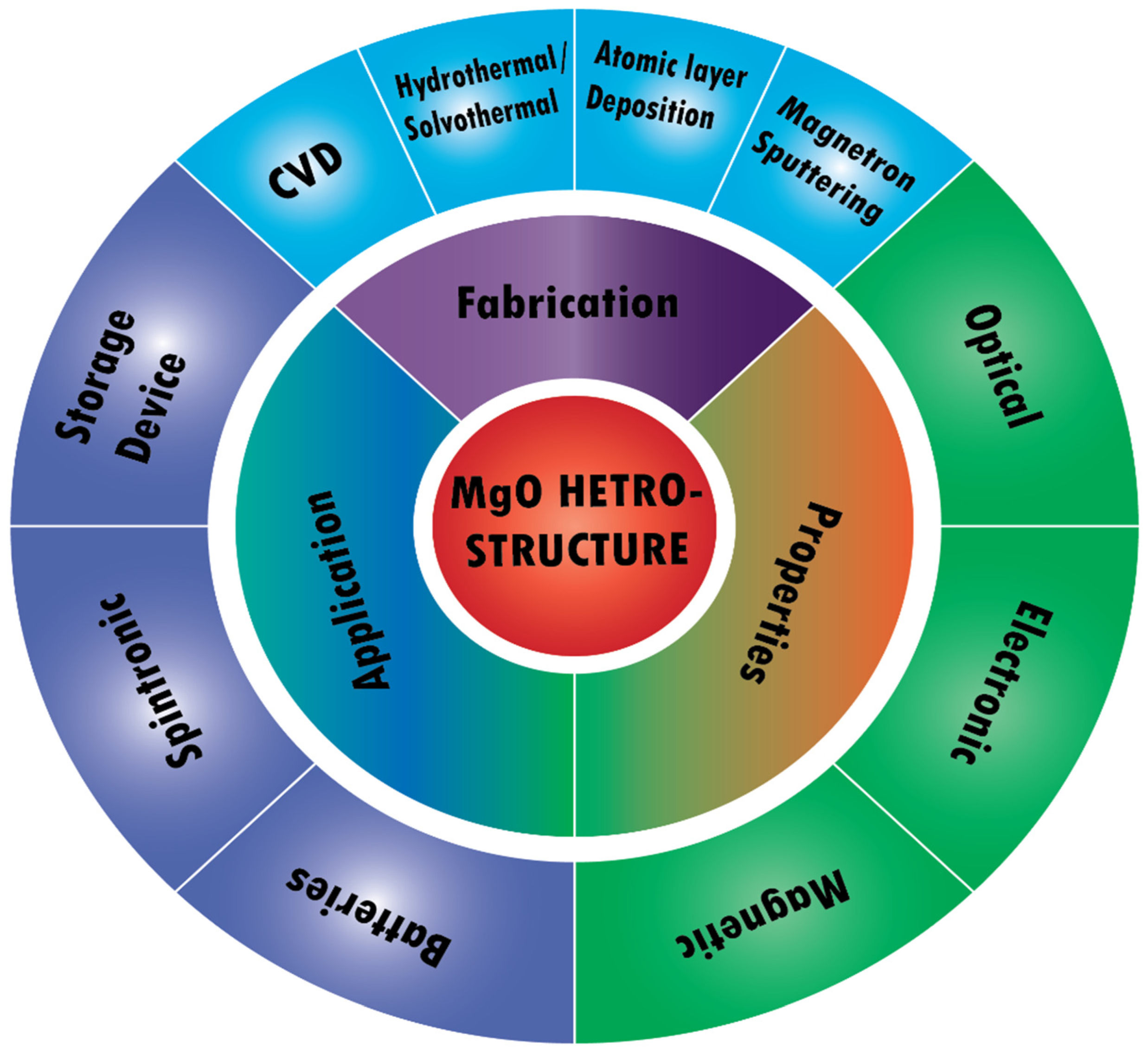
3. Magnesium Oxide
3.1. Basic
3.2. MgO Properties
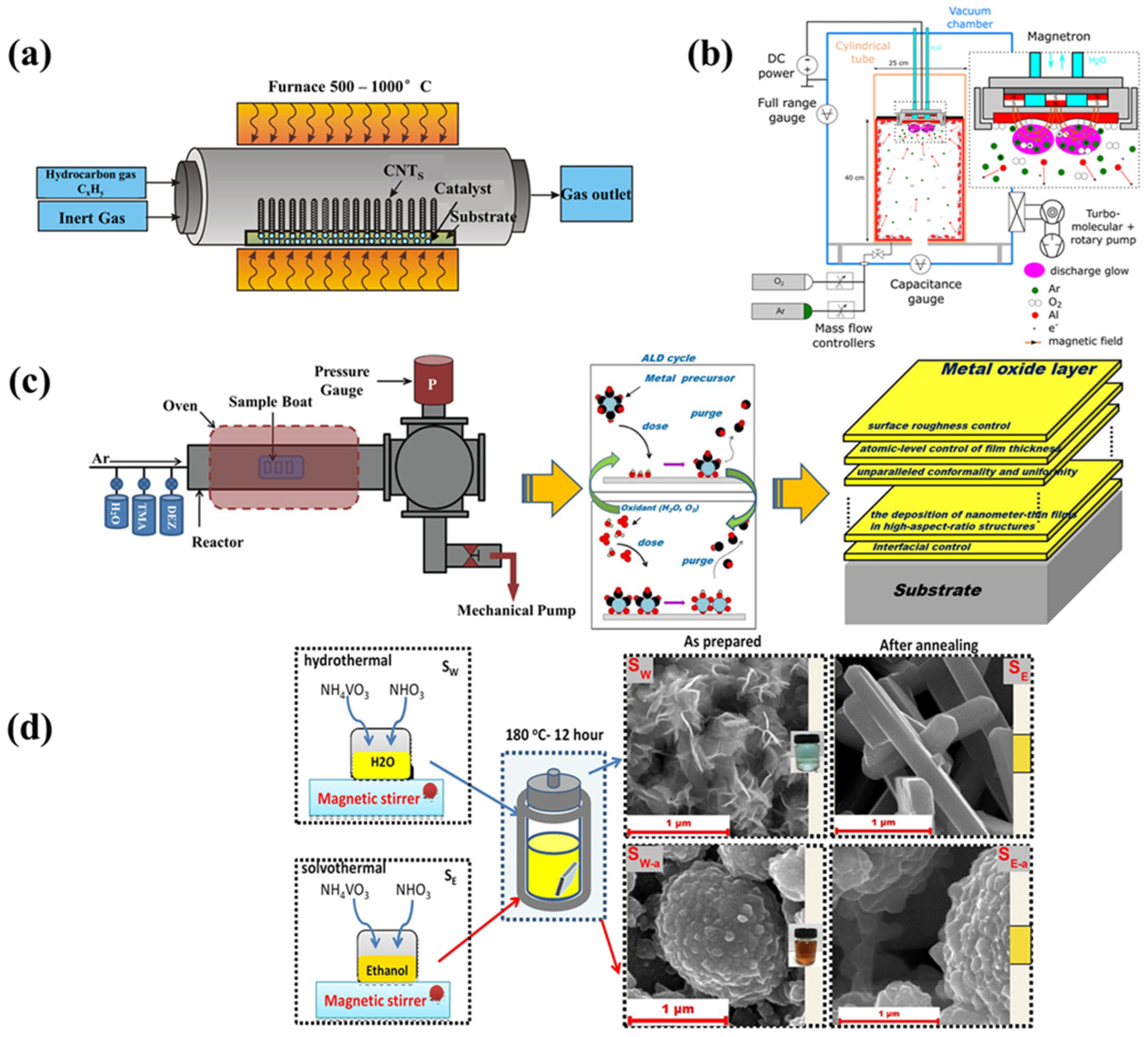
3.3. Fabrication Techniques
3.3.1. Chemical Vapor Deposition
3.3.2. Magnetron Sputtering
3.3.3. Atomic Layer Deposition (ALD)
3.3.4. Hydrothermal/Solvothermal Synthesis

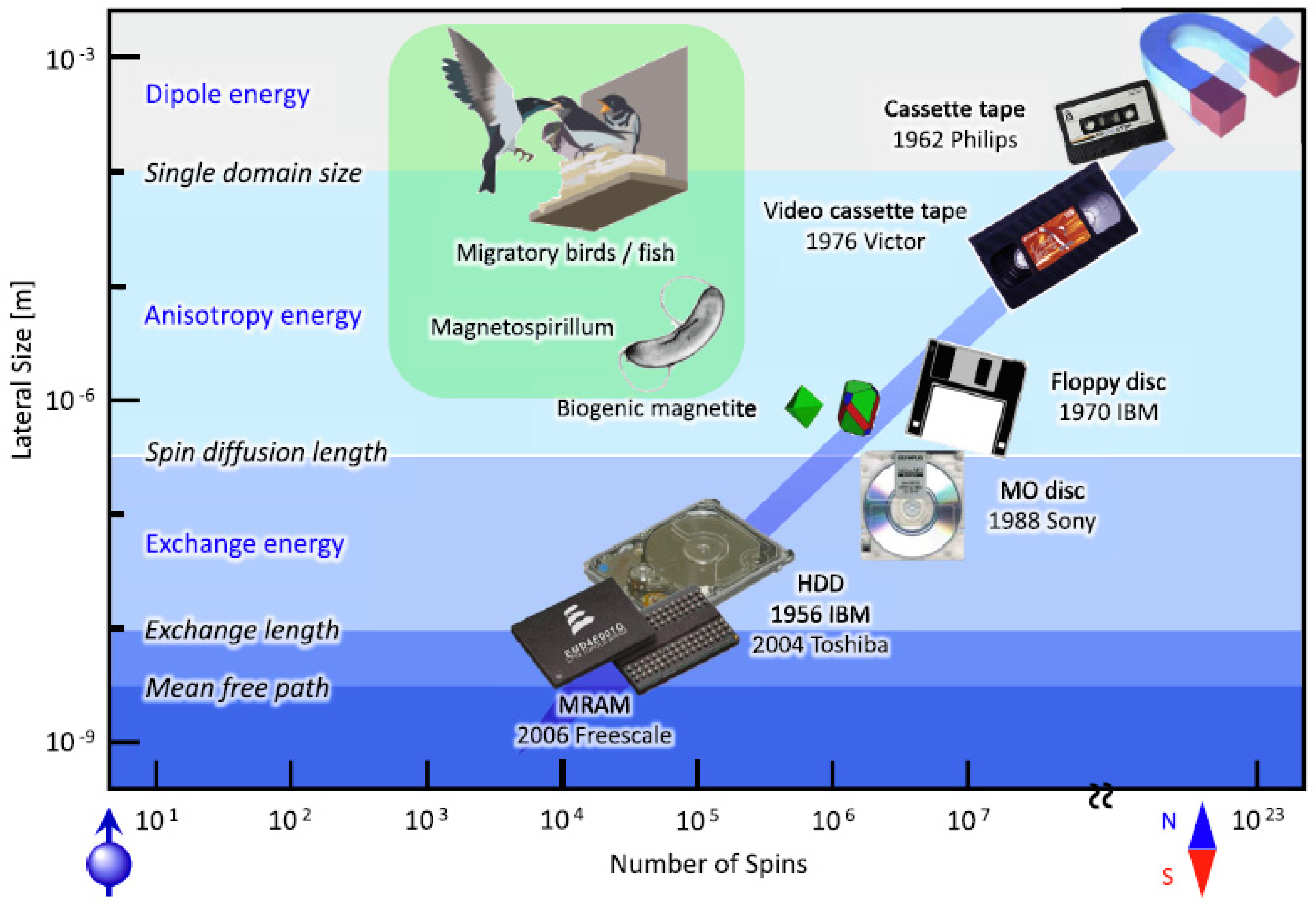
4. Magnetic Storage Applications
4.1. Magnetic Storage Devices Using MgO in Heterostructures
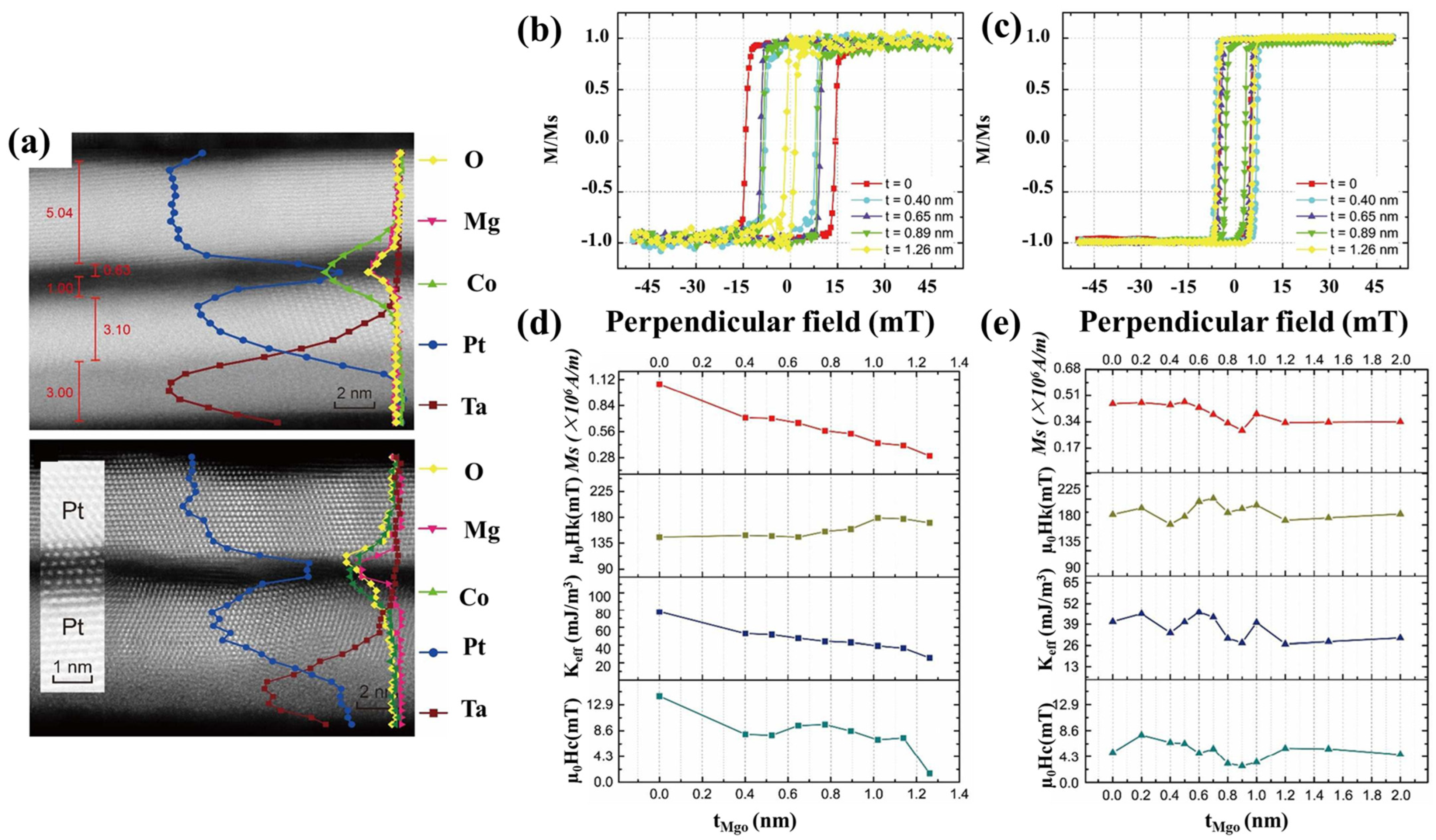
4.2. Magnetic Anisotropy of MgO Heterostructure
4.3. Perpendicular Magnetic Anisotropy
4.4. Anisotropy Voltage Control
4.5. Spin–Orbit Effects in MgO Heterostructures
5. Energy Storage Applications
5.1. Energy Storage Devices
5.2. Heterostructures’ Energy Storage Mechanisms
6. Conclusions and Prospects
Author Contributions
Funding
Institutional Review Board Statement
Acknowledgments
Conflicts of Interest
References
- Cai, W.; Yan, C.; Yao, Y.-X.; Xu, L.; Xu, R.; Jiang, L.-L.; Huang, J.-Q.; Zhang, Q. Rapid lithium diffusion in order@ disorder pathways for fast-charging graphite anodes. Small Struct. 2020, 1, 2000010. [Google Scholar] [CrossRef]
- Li, Y.; Zhang, J.; Chen, Q.; Xia, X.; Chen, M. Emerging of heterostructure materials in energy storage: A review. Adv. Mater. 2021, 33, 2100855. [Google Scholar] [CrossRef]
- Alferov, Z.I. The history and future of semiconductor heterostructures. Semiconductors 1998, 32, 1–14. [Google Scholar] [CrossRef]
- Peng, Q.; Hu, K.; Sa, B.; Zhou, J.; Wu, B.; Hou, X.; Sun, Z. Unexpected elastic isotropy in a black phosphorene/TiC2 van der Waals heterostructure with flexible Li-ion battery anode applications. Nano Res. 2017, 10, 3136–3150. [Google Scholar] [CrossRef]
- Einspruch, N.G. VLSI Electronics: Microstructure Science; Academic Press: Cambridge, MA, USA, 2014. [Google Scholar]
- Geim, A.K.; Grigorieva, I.V. Van der Waals heterostructures. Nature 2013, 499, 419–425. [Google Scholar] [CrossRef]
- Jariwala, D.; Sangwan, V.K.; Lauhon, L.J.; Marks, T.J.; Hersam, M.C. Emerging device applications for semiconducting two-dimensional transition metal dichalcogenides. ACS Nano 2014, 8, 1102–1120. [Google Scholar] [CrossRef] [Green Version]
- Kim, K.; Yankowitz, M.; Fallahazad, B.; Kang, S.; Movva, H.C.; Huang, S.; Larentis, S.; Corbet, C.M.; Taniguchi, T.; Watanabe, K. van der Waals heterostructures with high accuracy rotational alignment. Nano Lett. 2016, 16, 1989–1995. [Google Scholar] [CrossRef]
- Lee, Y.; Hwang, Y.; Chung, Y.-C. Achieving type I, II, and III heterojunctions using functionalized MXene. ACS Appl. Mater. Interfaces 2015, 7, 7163–7169. [Google Scholar] [CrossRef]
- Li, H.; Liu, H.; Li, C.; Liu, J.; Liu, J.; Yang, Q. Micro-scale spatial location engineering of COF–TiO 2 heterojunctions for visible light driven photocatalytic alcohol oxidation. J. Mater. Chem. A 2020, 8, 18745–18754. [Google Scholar] [CrossRef]
- Chen, S.; Hu, Y.; Meng, S.; Fu, X. Study on the separation mechanisms of photogenerated electrons and holes for composite photocatalysts g-C3N4-WO3. Appl. Catal. B Environ. 2014, 150, 564–573. [Google Scholar] [CrossRef]
- Zang, H.-Y.; Lan, Y.-Q.; Su, Z.-M.; Yang, G.-S.; Xu, G.-J.; Du, D.-Y.; Chen, L.; Yan, L.-K. Construction of a series of 0D, 2D and 3D inorganic–organic hybrid coordination polymers based on octamolybdate and 2-(2-pyridyl) imidazole and its derivative. Inorg. Chim. Acta 2010, 363, 118–126. [Google Scholar] [CrossRef]
- Kumari, A.; Singh, R.R. Encapsulation of highly confined CdSe quantum dots for defect free luminescence and improved stability. Phys. E Low-Dimens. Syst. Nanostructures 2017, 89, 77–85. [Google Scholar] [CrossRef]
- Qi, H.; Wang, L.; Sun, J.; Long, Y.; Hu, P.; Liu, F.; He, X. Production methods of van der Waals heterostructures based on transition metal dichalcogenides. Crystals 2018, 8, 35. [Google Scholar] [CrossRef] [Green Version]
- Ivanova, A. Nanoporous Metal Oxides Templated by Nanocrystalline Cellulose. Ph.D. Thesis, Ludwig Maximilian University of Munich, München, Germany, 2015. [Google Scholar]
- Xie, Y.; He, Y.; Irwin, P.L.; Jin, T.; Shi, X. Antibacterial activity and mechanism of action of zinc oxide nanoparticles against Campylobacter jejuni. Appl. Environ. Microbiol. 2011, 77, 2325–2331. [Google Scholar] [CrossRef] [Green Version]
- Xu, X.; Li, R.; Tang, C.; Wang, H.; Zhuang, X.; Liu, Y.; Kang, W.; Shi, L. Cellulose nanofiber-embedded sulfonated poly (ether sulfone) membranes for proton exchange membrane fuel cells. Carbohydr. Polym. 2018, 184, 299–306. [Google Scholar] [CrossRef]
- Ansari, A.A.; Kaushik, A.; Solanki, P.; Malhotra, B. Sol–gel derived nanoporous cerium oxide film for application to cholesterol biosensor. Electrochem. Commun. 2008, 10, 1246–1249. [Google Scholar] [CrossRef]
- Qingqing, W.; Gang, X.; Gaorong, H. Solvothermal synthesis and characterization of uniform CdS nanowires in high yield. J. Solid State Chem. 2005, 178, 2680–2685. [Google Scholar] [CrossRef]
- Wu, M.-C.; Corneille, J.S.; Estrada, C.A.; He, J.-W.; Goodman, D.W. Synthesis and characterization of ultra-thin MgO films on Mo (100). Chem. Phys. Lett. 1991, 182, 472–478. [Google Scholar] [CrossRef]
- Marfunin, A.S. Advanced Mineralogy: Volume 1 Composition, Structure, and Properties of Mineral Matter: Concepts, Results, and Problems; Springer Science & Business Media: Berlin/Heidelberg, Germany, 2012; Volume 1. [Google Scholar]
- Hornak, J.; Trnka, P.; Kadlec, P.; Michal, O.; Mentlík, V.; Šutta, P.; Csányi, G.M.; Tamus, Z.Á. Magnesium oxide nanoparticles: Dielectric properties, surface functionalization and improvement of epoxy-based composites insulating properties. Nanomaterials 2018, 8, 381. [Google Scholar] [CrossRef] [PubMed] [Green Version]
- Jin, C.; Kim, H.; Lee, W.I.; Lee, C. Ultraintense Luminescence in Semiconducting-Material-Sheathed MgO Nanorods. Adv. Mater. 2011, 23, 1982–1987. [Google Scholar] [CrossRef]
- Jin, C.; Kim, H.; Lee, C. Ultraintense short-wavelength emission from ZnO-sheathed MgO nanorods induced by subwavelength optical resonance cavity formation: Verification of previous hypothesis. ACS Appl. Mater. Interfaces 2012, 4, 1262–1266. [Google Scholar] [CrossRef]
- González, R.; Chen, Y. Deuteron diffusion and photoluminescence in lithium-doped MgO crystals. Phys. Rev. B 1987, 35, 8202. [Google Scholar] [CrossRef] [PubMed]
- Jin, C.; Lee, J.; Park, S.; Lee, C. Effects of passivation and postannealing on the photoluminescence properties of MgO/SiO2 core-shell nanorods. Cryst. Res. Technol. 2011, 46, 315–320. [Google Scholar] [CrossRef]
- Li, Q.; Zhang, S.; Wang, J.; Gao, H. Process analysis of MgO film on NdFeB magnet by sol–gel method. Surf. Eng. 2009, 25, 589–593. [Google Scholar] [CrossRef]
- Sharma, G.; Soni, R.; Jasuja, N.D. Phytoassisted synthesis of magnesium oxide nanoparticles with Swertia chirayaita. J. Taibah Univ. Sci. 2017, 11, 471–477. [Google Scholar] [CrossRef] [Green Version]
- Wilson, I. Magnesium oxide as a high-temperature insulant. IEE Proc. A (Phys. Sci. Meas. Instrum. Manag. Educ. Rev.) 1981, 128, 159–164. [Google Scholar] [CrossRef]
- Senbayram, M.; Gransee, A.; Wahle, V.; Thiel, H. Role of magnesium fertilisers in agriculture: Plant–soil continuum. Crop Pasture Sci. 2015, 66, 1219–1229. [Google Scholar] [CrossRef]
- Wang, J.; Novaro, O.; Bokhimi, X.; Lopez, T.; Gomez, R.; Navarrete, J.; Llanos, M.; Lopez-Salinas, E. Structural defects and acidic and basic sites in Sol− Gel MgO. J. Phys. Chem. B 1997, 101, 7448–7451. [Google Scholar] [CrossRef]
- Ding, Y.; Zhang, G.; Wu, H.; Hai, B.; Wang, L.; Qian, Y. Nanoscale magnesium hydroxide and magnesium oxide powders: Control over size, shape, and structure via hydrothermal synthesis. Chem. Mater. 2001, 13, 435–440. [Google Scholar] [CrossRef]
- Andritsch, T. Epoxy Based Nanodielectrics for High Voltage DC-Applications: Synthesis, Dielectric Properties and Space Charge Dynamics; Delft University of Technology: Delft, The Netherlands, 2010. [Google Scholar]
- Bindhu, M.; Umadevi, M.; Micheal, M.K.; Arasu, M.V.; Al-Dhabi, N.A. Structural, morphological and optical properties of MgO nanoparticles for antibacterial applications. Mater. Lett. 2016, 166, 19–22. [Google Scholar] [CrossRef]
- Calebrese, C.; Hui, L.; Schadler, L.S.; Nelson, J.K. A review on the importance of nanocomposite processing to enhance electrical insulation. IEEE Trans. Dielectr. Electr. Insul. 2011, 18, 938–945. [Google Scholar] [CrossRef]
- Dikshit, V.; Bhudolia, S.K.; Joshi, S.C. Multiscale polymer composites: A review of the interlaminar fracture toughness improvement. Fibers 2017, 5, 38. [Google Scholar] [CrossRef] [Green Version]
- Taurian, O.; Springborg, M.; Christensen, N. Self-consistent electronic structures of MgO and SrO. Solid State Commun. 1985, 55, 351–355. [Google Scholar] [CrossRef]
- Strijckmans, K.; Schelfhout, R.; Depla, D. Tutorial: Hysteresis during the reactive magnetron sputtering process. J. Appl. Phys. 2018, 124, 241101. [Google Scholar] [CrossRef]
- Liu, Y.; Zhang, S.; He, J.; Wang, Z.M.; Liu, Z. Recent progress in the fabrication, properties, and devices of heterostructures based on 2D materials. Nano-Micro Lett. 2019, 11, 1–24. [Google Scholar] [CrossRef]
- Sénateur, J.P.; Dubourdieu, C.; Weiss, F.; Rosina, M.; Abrutis, A. Pulsed injection MOCVD of functional electronic oxides. Adv. Funct. Mater. 2000, 10, 155–161. [Google Scholar]
- Dubourdieu, C.; Rosina, M.; Roussel, H.; Weiss, F.; Sénateur, J.; Hodeau, J. Pulsed liquid-injection metalorganic chemical vapor deposition of (La 0.7 Sr 0.3 MnO 3/SrTiO 3) 15 superlattices. Appl. Phys. Lett. 2001, 79, 1246–1248. [Google Scholar] [CrossRef]
- Dubourdieu, C.; Huot, G.; Gelard, I.; Roussel, H.; Lebedev, O.; Van Tendeloo, G. Thin films and superlattices of multiferroic hexagonal rare earth manganites. Philos. Mag. Lett. 2007, 87, 203–210. [Google Scholar] [CrossRef]
- Heil, S.; Langereis, E.; Roozeboom, F.; Kemmeren, A.; Pham, N.; Sarro, P.; Van De Sanden, M.; Kessels, W. Plasma-assisted atomic layer deposition of TiN films at low deposition temperature for high-aspect ratio applications. MRS Online Proc. Libr. (OPL) 2005, 863. [Google Scholar] [CrossRef]
- Cho, Y.; Jeong, M.; Park, J.; Hu, W.; Lim, J.; Chang, H. Charge Transporting Materials Grown by Atomic Layer Deposition in Perovskite Solar Cells. Energies 2021, 14, 1156. [Google Scholar] [CrossRef]
- Slewa, L.H.; Abbas, T.A.; Ahmed, N.M. Hydrothermal and solvothermal synthesis of nanorods and 3D (micro/nano) V2O5 on macro PSi substrate for pH-EGFET sensors. J. Mater. Sci. Mater. Electron. 2019, 30, 11193–11207. [Google Scholar] [CrossRef]
- Zaytseva, O.; Neumann, G. Carbon nanomaterials: Production, impact on plant development, agricultural and environmental applications. Chem. Biol. Technol. Agric. 2016, 3, 1–26. [Google Scholar] [CrossRef] [Green Version]
- Oldham, C.J.; Gong, B.; Spagnola, J.C.; Jur, J.S.; Senecal, K.J.; Godfrey, T.A.; Parsons, G.N. Encapsulation and chemical resistance of electrospun nylon nanofibers coated using integrated atomic and molecular layer deposition. J. Electrochem. Soc. 2011, 158, D549. [Google Scholar] [CrossRef]
- Liang, S.H.; Gay, I.D. A 13C solid-state NMR study of the chemisorption and decomposition of ethanol on MgO. J. Catal. 1986, 101, 293–300. [Google Scholar] [CrossRef]
- Yang, P.; Lieber, C.M. Nanorod-superconductor composites: A pathway to materials with high critical current densities. Science 1996, 273, 1836–1840. [Google Scholar] [CrossRef]
- Yanagida, T.; Nagashima, K.; Tanaka, H.; Kawai, T. Mechanism of critical catalyst size effect on MgO nanowire growth by pulsed laser deposition. J. Appl. Phys. 2008, 104, 016101. [Google Scholar] [CrossRef] [Green Version]
- Galstyan, V. Porous TiO2-based gas sensors for cyber chemical systems to provide security and medical diagnosis. Sensors 2017, 17, 2947. [Google Scholar] [CrossRef] [Green Version]
- Ni, S.; Yu, Q.; Huang, Y.; Wang, J.; Li, L.; Yu, C.; Guo, F.; Wu, H.; Lu, W.; Zhang, X. Heterostructured TiO 2/MgO nanowire arrays for self-powered UV photodetectors. RSC Adv. 2016, 6, 85951–85957. [Google Scholar] [CrossRef]
- Bocdanov, A.; Hubert, A. The properties of isolated magnetic vortices. Phys. Status Solidi 1994, 186, 527–543. [Google Scholar] [CrossRef]
- Parkin, S.S.; Hayashi, M.; Thomas, L. Magnetic domain-wall racetrack memory. Science 2008, 320, 190–194. [Google Scholar] [CrossRef]
- Cao, A.; Zhang, X.; Koopmans, B.; Peng, S.; Zhang, Y.; Wang, Z.; Yan, S.; Yang, H.; Zhao, W. Tuning the Dzyaloshinskii–Moriya interaction in Pt/Co/MgO heterostructures through the MgO thickness. Nanoscale 2018, 10, 12062–12067. [Google Scholar] [CrossRef] [Green Version]
- Lee, H.-Y.; Kim, S.; Park, J.-Y.; Oh, Y.-W.; Park, S.-Y.; Ham, W.; Kotani, Y.; Nakamura, T.; Suzuki, M.; Ono, T. Enhanced spin–orbit torque via interface engineering in Pt/CoFeB/MgO heterostructures. APL Mater. 2019, 7, 031110. [Google Scholar] [CrossRef] [Green Version]
- Torrejon, J.; Kim, J.; Sinha, J.; Mitani, S.; Hayashi, M.; Yamanouchi, M.; Ohno, H. Interface control of the magnetic chirality in CoFeB/MgO heterostructures with heavy-metal underlayers. Nat. Commun. 2014, 5, 1–8. [Google Scholar] [CrossRef] [PubMed]
- Haldar, K.K.; Biswas, R.; Tanwar, S.; Sen, T.; Lahtinen, J. One-pot synthesis of Au embedded ZnO nanorods composite heterostructures with excellent photocatalytic properties. ChemistrySelect 2018, 3, 7882–7890. [Google Scholar] [CrossRef]
- Han, S.; Yu, L.; Zhang, H.; Chu, Z.; Chen, X.; Xi, H.; Long, J. Gold Plasmon-Enhanced Solar Hydrogen Production over SrTiO3/TiO2 Heterostructures. ChemCatChem 2019, 11, 6203–6207. [Google Scholar] [CrossRef]
- Ma, L.; Lin, Z.; Lin, J.; Zhang, Y.; Hu, L.; Guo, T. Large-scale growth of ultrathin MgO nanowires and evaluate their field emission properties. Phys. E Low-Dimens. Syst. Nanostructures 2009, 41, 1500–1503. [Google Scholar] [CrossRef]
- Li, Z.; Mi, W.; Bai, H. The contribution of distinct response characteristics of Fe atoms to switching of magnetic anisotropy in Fe4N/MgO heterostructures. Appl. Phys. Lett. 2018, 113, 132401. [Google Scholar] [CrossRef]
- Ong, P.; Kioussis, N.; Amiri, P.K.; Wang, K.; Carman, G.P. Strain control magnetocrystalline anisotropy of Ta/FeCo/MgO heterostructures. J. Appl. Phys. 2015, 117, 17B518. [Google Scholar] [CrossRef]
- Ramaswamy, R.; Qiu, X.; Dutta, T.; Pollard, S.D.; Yang, H. Hf thickness dependence of spin-orbit torques in Hf/CoFeB/MgO heterostructures. Appl. Phys. Lett. 2016, 108, 202406. [Google Scholar] [CrossRef]
- Ong, P.; Kioussis, N.; Amiri, P.K.; Wang, K. Electric-field-driven magnetization switching and nonlinear magnetoelasticity in Au/FeCo/MgO heterostructures. Sci. Rep. 2016, 6, 1–8. [Google Scholar]
- Wen, Z.; Sukegawa, H.; Seki, T.; Kubota, T.; Takanashi, K.; Mitani, S. Voltage control of magnetic anisotropy in epitaxial Ru/Co2FeAl/MgO heterostructures. Sci. Rep. 2017, 7, 45026. [Google Scholar] [CrossRef] [PubMed]
- Kanai, S.; Matsukura, F.; Ohno, H. Electric-field-induced magnetization switching in CoFeB/MgO magnetic tunnel junctions with high junction resistance. Appl. Phys. Lett. 2016, 108, 192406. [Google Scholar] [CrossRef]
- Grezes, C.; Ebrahimi, F.; Alzate, J.; Cai, X.; Katine, J.; Langer, J.; Ocker, B.; Khalili Amiri, P.; Wang, K. Ultra-low switching energy and scaling in electric-field-controlled nanoscale magnetic tunnel junctions with high resistance-area product. Appl. Phys. Lett. 2016, 108, 012403. [Google Scholar] [CrossRef] [Green Version]
- Xiang, Q.; Wen, Z.; Sukegawa, H.; Kasai, S.; Seki, T.; Kubota, T.; Takanashi, K.; Mitani, S. Nonlinear electric field effect on perpendicular magnetic anisotropy in Fe/MgO interfaces. J. Phys. D Appl. Phys. 2017, 50, 40LT04. [Google Scholar] [CrossRef]
- Chen, W.-Z.; Zhang, M.; Liu, Y.; Yao, X.-M.; Liu, P.-Y.; Liu, Z.; He, J.; Wang, Y.-Q. Super-Hydrophilic MgO/NiCo2S4 Heterostructure for High-Efficient Oxygen Evolution Reaction in Neutral Electrolytes. Appl. Catal. B Environ. 2022, 312, 121432. [Google Scholar] [CrossRef]
- Almasi, H.; Xu, M.; Xu, Y.; Newhouse-Illige, T.; Wang, W. Effect of Mo insertion layers on the magnetoresistance and perpendicular magnetic anisotropy in Ta/CoFeB/MgO junctions. Appl. Phys. Lett. 2016, 109, 032401. [Google Scholar] [CrossRef]
- Wang, M.; Song, Y.; Sun, Z.; Shao, Y.; Wei, C.; Xia, Z.; Tian, Z.; Liu, Z.; Sun, J. Conductive and catalytic VTe2@ MgO heterostructure as effective polysulfide promotor for lithium–sulfur batteries. ACS Nano 2019, 13, 13235–13243. [Google Scholar] [CrossRef]
- Iida, Y.; Xiang, Q.; Okabayashi, J.; Scheike, T.; Sukegawa, H.; Mitani, S. Effect of tungsten doping on perpendicular magnetic anisotropy and its voltage effect in single crystal Fe/MgO (001) interfaces. J. Phys. D Appl. Phys. 2020, 53, 124001. [Google Scholar] [CrossRef]
- Xiang, Q.; Mandal, R.; Sukegawa, H.; Takahashi, Y.K.; Mitani, S. Large perpendicular magnetic anisotropy in epitaxial Fe/MgAl2O4 (001) heterostructures. Appl. Phys. Express 2018, 11, 063008. [Google Scholar] [CrossRef] [Green Version]
- Ahn, J.; Ma, J.; Lee, D.; Lin, Q.; Park, Y.; Lee, O.; Sim, S.; Lee, K.; Yoo, G.; Heo, J. Ultrahigh deep-ultraviolet responsivity of a β-Ga2O3/MgO heterostructure-based phototransistor. ACS Photonics 2021, 8, 557–566. [Google Scholar] [CrossRef]
- Hirohata, A.; Takanashi, K. Future perspectives for spintronic devices. J. Phys. D Appl. Phys. 2014, 47, 193001. [Google Scholar] [CrossRef]
- Ryu, K.-S.; Thomas, L.; Yang, S.-H.; Parkin, S. Chiral spin torque at magnetic domain walls. Nat. Nanotechnol. 2013, 8, 527–533. [Google Scholar] [CrossRef]
- Chen, G.; Zhu, J.; Quesada, A.; Li, J.; N’Diaye, A.; Huo, Y.; Ma, T.; Chen, Y.; Kwon, H.; Won, C. Novel chiral magnetic domain wall structure in Fe/Ni/Cu (001) films. Phys. Rev. Lett. 2013, 110, 177204. [Google Scholar] [CrossRef] [Green Version]
- Fert, A.; Cros, V.; Sampaio, J. Skyrmions on the track. Nat. Nanotechnol. 2013, 8, 152–156. [Google Scholar] [CrossRef] [PubMed]
- Emori, S.; Bauer, U.; Ahn, S.-M.; Martinez, E.; Beach, G.S. Current-driven dynamics of chiral ferromagnetic domain walls. Nat. Mater. 2013, 12, 611–616. [Google Scholar] [CrossRef] [Green Version]
- Chappert, C.; Fert, A.; Van Dau, F.N. The emergence of spin electronics in data storage. Nanosci. Technol. A Collect. Rev. Nat. J. 2010, 147–157. [Google Scholar]
- Shiota, Y.; Maruyama, T.; Nozaki, T.; Shinjo, T.; Shiraishi, M.; Suzuki, Y. Voltage-assisted magnetization switching in ultrathin Fe80Co20 alloy layers. Appl. Phys. Express 2009, 2, 063001. [Google Scholar] [CrossRef] [Green Version]
- Maruyama, T.; Shiota, Y.; Nozaki, T.; Ohta, K.; Toda, N.; Mizuguchi, M.; Tulapurkar, A.; Shinjo, T.; Shiraishi, M.; Mizukami, S. Large voltage-induced magnetic anisotropy change in a few atomic layers of iron. Nat. Nanotechnol. 2009, 4, 158–161. [Google Scholar] [CrossRef] [PubMed]
- Wang, W.-G.; Li, M.; Hageman, S.; Chien, C. Electric-field-assisted switching in magnetic tunnel junctions. Nat. Mater. 2012, 11, 64–68. [Google Scholar] [CrossRef]
- Lupascu, A.; Clancy, J.; Gretarsson, H.; Nie, Z.; Nichols, J.; Terzic, J.; Cao, G.; Seo, S.; Islam, Z.; Upton, M. Tuning magnetic coupling in Sr 2 IrO 4 thin films with epitaxial strain. Phys. Rev. Lett. 2014, 112, 147201. [Google Scholar] [CrossRef] [PubMed] [Green Version]
- Huang, W.; Zhu, J.; Zeng, H.; Wei, X.; Zhang, Y.; Li, Y. Strain induced magnetic anisotropy in highly epitaxial CoFe2O4 thin films. Appl. Phys. Lett. 2006, 89, 262506. [Google Scholar] [CrossRef]
- Jung, C.; Yamada, H.; Kawasaki, M.; Tokura, Y. Magnetic anisotropy control of SrRuO 3 films by tunable epitaxial strain. Appl. Phys. Lett. 2004, 84, 2590–2592. [Google Scholar] [CrossRef]
- Du, C.; Adur, R.; Wang, H.; Hauser, A.J.; Yang, F.; Hammel, P.C. Control of magnetocrystalline anisotropy by epitaxial strain in double perovskite Sr 2 FeMoO 6 films. Phys. Rev. Lett. 2013, 110, 147204. [Google Scholar] [CrossRef] [Green Version]
- Stone, P.; Dreher, L.; Beeman, J.; Yu, K.; Brandt, M.; Dubon, O. Interplay of epitaxial strain and perpendicular magnetic anisotropy in insulating ferromagnetic Ga1−xMnxP1−yNy. Phys. Rev. B 2010, 81, 205210. [Google Scholar] [CrossRef]
- Burkert, T.; Nordström, L.; Eriksson, O.; Heinonen, O. Giant magnetic anisotropy in tetragonal FeCo alloys. Phys. Rev. Lett. 2004, 93, 027203. [Google Scholar] [CrossRef] [PubMed]
- Blochl, P.; Bl, E. ochl and PE Bl€ ochl. Phys. Rev. B Condens. Matt 1994, 50, 163. [Google Scholar]
- Kokado, S.; Fujima, N.; Harigaya, K.; Shimizu, H.; Sakuma, A. Theoretical analysis of highly spin-polarized transport in the iron nitride Fe 4 N. Phys. Rev. B 2006, 73, 172410. [Google Scholar] [CrossRef] [Green Version]
- Mi, W.; Guo, Z.; Feng, X.; Bai, H. Reactively sputtered epitaxial γ’-Fe4N films: Surface morphology, microstructure, magnetic and electrical transport properties. Acta Mater. 2013, 61, 6387–6395. [Google Scholar] [CrossRef]
- Sunaga, K.; Tsunoda, M.; Komagaki, K.; Uehara, Y.; Takahashi, M. Inverse tunnel magnetoresistance in magnetic tunnel junctions with an Fe 4 N electrode. J. Appl. Phys. 2007, 102, 013917. [Google Scholar] [CrossRef]
- Komasaki, Y.; Tsunoda, M.; Isogami, S.; Takahashi, M. 75% inverse magnetoresistance at room temperature in Fe 4 N/MgO/CoFeB magnetic tunnel junctions fabricated on Cu underlayer. J. Appl. Phys. 2009, 105, 07C928. [Google Scholar] [CrossRef]
- Tsunoda, M.; Chiba, R.; Kabara, K. Fabrication of MgAl2O4 tunnel barrier by radio frequency-sputtering method and magnetoresistance effect through it with Fe or Fe4N ferromagnetic electrode. J. Appl. Phys. 2015, 117, 17D703. [Google Scholar] [CrossRef]
- Yang, H.; Chshiev, M.; Dieny, B.; Lee, J.; Manchon, A.; Shin, K. First-principles investigation of the very large perpendicular magnetic anisotropy at Fe| MgO and Co| MgO interfaces. Phys. Rev. B 2011, 84, 054401. [Google Scholar] [CrossRef] [Green Version]
- Hallal, A.; Yang, H.; Dieny, B.; Chshiev, M. Anatomy of perpendicular magnetic anisotropy in Fe/MgO magnetic tunnel junctions: First-principles insight. Phys. Rev. B 2013, 88, 184423. [Google Scholar] [CrossRef] [Green Version]
- Yang, H.; Chshiev, M.; Kalitsov, A.; Schuhl, A.; Butler, W. Effect of structural relaxation and oxidation conditions on interlayer exchange coupling in Fe| MgO| Fe tunnel junctions. Appl. Phys. Lett. 2010, 96, 262509. [Google Scholar] [CrossRef] [Green Version]
- Nazir, S.; Jiang, S.; Cheng, J.; Yang, K. Enhanced interfacial perpendicular magnetic anisotropy in Fe/MgO heterostructure via interfacial engineering. Appl. Phys. Lett. 2019, 114, 072407. [Google Scholar] [CrossRef]
- Gao, X.; Yang, B.; Devaux, X.; Yang, H.; Liu, J.; Liang, S.; Stoffel, M.; Pasquier, L.; Hyot, B.; Grenier, A. Evidence of a strong perpendicular magnetic anisotropy in Au/Co/MgO/GaN heterostructures. Nanoscale Adv. 2019, 1, 4466–4475. [Google Scholar] [CrossRef] [Green Version]
- Buyanova, I.; Izadifard, M.; Chen, W.M.; Kim, J.; Ren, F.; Thaler, G.; Abernathy, C.; Pearton, S.; Pan, C.C.; Chen, G.T. Spin injection and spin loss in GaMnN/InGaN Light-Emitting Diodes. AIP Conf. Proc. 2005, 772, 1399–1400. [Google Scholar]
- Ham, M.-H.; Yoon, S.; Park, Y.; Bian, L.; Ramsteiner, M.; Myoung, J.-M. Electrical spin injection from room-temperature ferromagnetic (Ga, Mn) N in nitride-based spin-polarized light-emitting diodes. J. Phys. Condens. Matter 2006, 18, 7703. [Google Scholar] [CrossRef] [PubMed]
- Banerjee, D.; Adari, R.; Sankaranarayan, S.; Kumar, A.; Ganguly, S.; Aldhaheri, R.; Hussain, M.; Balamesh, A.; Saha, D. Electrical spin injection using GaCrN in a GaN based spin light emitting diode. Appl. Phys. Lett. 2013, 103, 242408. [Google Scholar] [CrossRef] [Green Version]
- Chen, J.; Ho, C.; Lu, M.; Chu, L.; Chen, K.; Chu, S.; Chen, W.; Mou, C.; Chen, Y. Efficient spin-light emitting diodes based on InGaN/GaN quantum disks at room temperature: A new self-polarized paradigm. Nano Lett. 2014, 14, 3130–3137. [Google Scholar] [CrossRef]
- Chen, J.-Y.; Wong, T.-M.; Chang, C.-W.; Dong, C.-Y.; Chen, Y.-F. Self-polarized spin-nanolasers. Nat. Nanotechnol. 2014, 9, 845–850. [Google Scholar] [CrossRef]
- Bhattacharya, A.; Baten, Z.; Frost, T.; Bhattacharya, P. Room temperature GaN-based edge-emitting spin-polarized light emitting diode. IEEE Photonics Technol. Lett. 2017, 29, 338–341. [Google Scholar] [CrossRef]
- Bhattacharya, A.; Baten, M.Z.; Iorsh, I.; Frost, T.; Kavokin, A.; Bhattacharya, P. Room-temperature spin polariton diode laser. Phys. Rev. Lett. 2017, 119, 067701. [Google Scholar] [CrossRef]
- Mazzucato, S.; Zhang, T.; Carrère, H.; Lagarde, D.; Boonpeng, P.; Arnoult, A.; Lacoste, G.; Balocchi, A.; Amand, T.; Fontaine, C. Electron spin dynamics and g-factor in GaAsBi. Appl. Phys. Lett. 2013, 102, 252107. [Google Scholar] [CrossRef]
- Amiri, P.K.; Alzate, J.G.; Cai, X.Q.; Ebrahimi, F.; Hu, Q.; Wong, K.; Grèzes, C.; Lee, H.; Yu, G.; Li, X. Electric-field-controlled magnetoelectric RAM: Progress, challenges, and scaling. IEEE Trans. Magn. 2015, 51, 1–7. [Google Scholar] [CrossRef]
- Matsukura, F.; Tokura, Y.; Ohno, H. Control of magnetism by electric fields. Nat. Nanotechnol. 2015, 10, 209–220. [Google Scholar] [CrossRef]
- Locatelli, N.; Cros, V.; Grollier, J. Spin-torque building blocks. Nat. Mater. 2014, 13, 11–20. [Google Scholar] [CrossRef]
- Shiota, Y.; Nozaki, T.; Bonell, F.; Murakami, S.; Shinjo, T.; Suzuki, Y. Induction of coherent magnetization switching in a few atomic layers of FeCo using voltage pulses. Nat. Mater. 2012, 11, 39–43. [Google Scholar] [CrossRef]
- Kanai, S.; Yamanouchi, M.; Ikeda, S.; Nakatani, Y.; Matsukura, F.; Ohno, H. Electric field-induced magnetization reversal in a perpendicular-anisotropy CoFeB-MgO magnetic tunnel junction. Appl. Phys. Lett. 2012, 101, 122403. [Google Scholar] [CrossRef]
- Shiota, Y.; Bonell, F.; Miwa, S.; Mizuochi, N.; Shinjo, T.; Suzuki, Y. Opposite signs of voltage-induced perpendicular magnetic anisotropy change in CoFeB| MgO junctions with different underlayers. Appl. Phys. Lett. 2013, 103, 082410. [Google Scholar] [CrossRef]
- Kanai, S.; Nakatani, Y.; Yamanouchi, M.; Ikeda, S.; Sato, H.; Matsukura, F.; Ohno, H. Magnetization switching in a CoFeB/MgO magnetic tunnel junction by combining spin-transfer torque and electric field-effect. Appl. Phys. Lett. 2014, 104, 212406. [Google Scholar] [CrossRef]
- Liu, H.; Wang, R.; Guo, P.; Wen, Z.; Feng, J.; Wei, H.; Han, X.; Ji, Y.; Zhang, S. Manipulation of magnetization switching and tunnel magnetoresistance via temperature and voltage control. Sci. Rep. 2015, 5, 18269. [Google Scholar] [CrossRef] [PubMed] [Green Version]
- Skowroński, W.; Nozaki, T.; Shiota, Y.; Tamaru, S.; Yakushiji, K.; Kubota, H.; Fukushima, A.; Yuasa, S.; Suzuki, Y. Perpendicular magnetic anisotropy of Ir/CoFeB/MgO trilayer system tuned by electric fields. Appl. Phys. Express 2015, 8, 053003. [Google Scholar] [CrossRef]
- Nozaki, T.; Shiota, Y.; Shiraishi, M.; Shinjo, T.; Suzuki, Y. Voltage-induced perpendicular magnetic anisotropy change in magnetic tunnel junctions. Appl. Phys. Lett. 2010, 96, 022506. [Google Scholar] [CrossRef]
- Nozaki, T.; Yakushiji, K.; Tamaru, S.; Sekine, M.; Matsumoto, R.; Konoto, M.; Kubota, H.; Fukushima, A.; Yuasa, S. Voltage-induced magnetic anisotropy changes in an ultrathin FeB layer sandwiched between two MgO layers. Appl. Phys. Express 2013, 6, 073005. [Google Scholar] [CrossRef]
- Nozaki, T.; Kozioł-Rachwał, A.; Skowroński, W.; Zayets, V.; Shiota, Y.; Tamaru, S.; Kubota, H.; Fukushima, A.; Yuasa, S.; Suzuki, Y. Large voltage-induced changes in the perpendicular magnetic anisotropy of an MgO-based tunnel junction with an ultrathin Fe layer. Phys. Rev. Appl. 2016, 5, 044006. [Google Scholar] [CrossRef] [Green Version]
- Wen, Z.; Sukegawa, H.; Mitani, S.; Inomata, K. Perpendicular magnetization of Co2FeAl full-Heusler alloy films induced by MgO interface. Appl. Phys. Lett. 2011, 98, 242507. [Google Scholar] [CrossRef]
- Li, X.; Yin, S.; Liu, Y.; Zhang, D.; Xu, X.; Miao, J.; Jiang, Y. Perpendicular magnetic anisotropy of full-Heusler films in Pt/Co2FeAl/MgO trilayers. Appl. Phys. Express 2011, 4, 043006. [Google Scholar] [CrossRef] [Green Version]
- Wen, Z.; Sukegawa, H.; Furubayashi, T.; Koo, J.; Inomata, K.; Mitani, S.; Hadorn, J.P.; Ohkubo, T.; Hono, K. A 4-Fold-Symmetry Hexagonal Ruthenium for Magnetic Heterostructures Exhibiting Enhanced Perpendicular Magnetic Anisotropy and Tunnel Magnetoresistance. Adv. Mater. 2014, 26, 6483–6490. [Google Scholar] [CrossRef] [PubMed] [Green Version]
- Bai, Z.; Shen, L.; Cai, Y.; Wu, Q.; Zeng, M.; Han, G.; Feng, Y.P. Magnetocrystalline anisotropy and its electric-field-assisted switching of Heusler-compound-based perpendicular magnetic tunnel junctions. New J. Phys. 2014, 16, 103033. [Google Scholar] [CrossRef]
- Greer, A.; Gray, A.; Kanai, S.; Kaiser, A.; Ueda, S.; Yamashita, Y.; Bordel, C.; Palsson, G.; Maejima, N.; Yang, S.-H. Observation of boron diffusion in an annealed Ta/CoFeB/MgO magnetic tunnel junction with standing-wave hard x-ray photoemission. Appl. Phys. Lett. 2012, 101, 202402. [Google Scholar] [CrossRef] [Green Version]
- Sinha, J.; Gruber, M.; Kodzuka, M.; Ohkubo, T.; Mitani, S.; Hono, K.; Hayashi, M. Influence of boron diffusion on the perpendicular magnetic anisotropy in Ta| CoFeB| MgO ultrathin films. J. Appl. Phys. 2015, 117, 043913. [Google Scholar] [CrossRef]
- Liu, L.; Pai, C.-F.; Li, Y.; Tseng, H.; Ralph, D.; Buhrman, R. Spin-torque switching with the giant spin Hall effect of tantalum. Science 2012, 336, 555–558. [Google Scholar] [CrossRef] [PubMed] [Green Version]
- Miron, I.M.; Garello, K.; Gaudin, G.; Zermatten, P.-J.; Costache, M.V.; Auffret, S.; Bandiera, S.; Rodmacq, B.; Schuhl, A.; Gambardella, P. Perpendicular switching of a single ferromagnetic layer induced by in-plane current injection. Nature 2011, 476, 189–193. [Google Scholar] [CrossRef]
- Pai, C.-F.; Liu, L.; Li, Y.; Tseng, H.; Ralph, D.; Buhrman, R. Spin transfer torque devices utilizing the giant spin Hall effect of tungsten. Appl. Phys. Lett. 2012, 101, 122404. [Google Scholar] [CrossRef]
- Fan, Y.; Upadhyaya, P.; Kou, X.; Lang, M.; Takei, S.; Wang, Z.; Tang, J.; He, L.; Chang, L.-T.; Montazeri, M. Magnetization switching through giant spin–orbit torque in a magnetically doped topological insulator heterostructure. Nat. Mater. 2014, 13, 699–704. [Google Scholar] [CrossRef]
- Wang, Y.; Deorani, P.; Banerjee, K.; Koirala, N.; Brahlek, M.; Oh, S.; Yang, H. Topological surface states originated spin-orbit torques in Bi 2 Se 3. Phys. Rev. Lett. 2015, 114, 257202. [Google Scholar] [CrossRef] [Green Version]
- Qiu, X.; Narayanapillai, K.; Wu, Y.; Deorani, P.; Yang, D.-H.; Noh, W.-S.; Park, J.-H.; Lee, K.-J.; Lee, H.-W.; Yang, H. Spin–orbit-torque engineering via oxygen manipulation. Nat. Nanotechnol. 2015, 10, 333–338. [Google Scholar] [CrossRef]
- Akyol, M.; Alzate, J.G.; Yu, G.; Upadhyaya, P.; Wong, K.L.; Ekicibil, A.; Khalili Amiri, P.; Wang, K.L. Effect of the oxide layer on current-induced spin-orbit torques in Hf| CoFeB| MgO and Hf| CoFeB| TaOx structures. Appl. Phys. Lett. 2015, 106, 032406. [Google Scholar] [CrossRef]
- Jiang, A.; Yohannan, A.; Nnolim, N.O.; Tyson, T.A.; Axe, L.; Lee, S.L.; Cote, P. Investigation of the structure of β-tantalum. Thin Solid Film. 2003, 437, 116–122. [Google Scholar] [CrossRef] [Green Version]
- Nguyen, M.-H.; Ralph, D.; Buhrman, R. Spin torque study of the spin Hall conductivity and spin diffusion length in platinum thin films with varying resistivity. Phys. Rev. Lett. 2016, 116, 126601. [Google Scholar] [CrossRef]
- Diao, Z.; Apalkov, D.; Pakala, M.; Ding, Y.; Panchula, A.; Huai, Y. Spin transfer switching and spin polarization in magnetic tunnel junctions with MgO and AlO x barriers. Appl. Phys. Lett. 2005, 87, 232502. [Google Scholar] [CrossRef] [Green Version]
- Ikeda, S.; Hayakawa, J.; Ashizawa, Y.; Lee, Y.; Miura, K.; Hasegawa, H.; Tsunoda, M.; Matsukura, F.; Ohno, H. Tunnel magnetoresistance of 604% at 300 K by suppression of Ta diffusion in CoFeB/MgO/CoFeB pseudo-spin-valves annealed at high temperature. Appl. Phys. Lett. 2008, 93, 082508. [Google Scholar] [CrossRef]
- Conte, R.L.; Martinez, E.; Hrabec, A.; Lamperti, A.; Schulz, T.; Nasi, L.; Lazzarini, L.; Mantovan, R.; Maccherozzi, F.; Dhesi, S. Role of B diffusion in the interfacial Dzyaloshinskii-Moriya interaction in Ta/Co20Fe60B20/MgO nanowires. Phys. Rev. B 2015, 91, 014433. [Google Scholar] [CrossRef]
- Woo, S.; Litzius, K.; Krüger, B.; Im, M.-Y.; Caretta, L.; Richter, K.; Mann, M.; Krone, A.; Reeve, R.M.; Weigand, M. Observation of room-temperature magnetic skyrmions and their current-driven dynamics in ultrathin metallic ferromagnets. Nat. Mater. 2016, 15, 501–506. [Google Scholar] [CrossRef] [PubMed]
- Litzius, K.; Lemesh, I.; Krüger, B.; Bassirian, P.; Caretta, L.; Richter, K.; Büttner, F.; Sato, K.; Tretiakov, O.A.; Förster, J. Skyrmion Hall effect revealed by direct time-resolved X-ray microscopy. Nat. Phys. 2017, 13, 170–175. [Google Scholar] [CrossRef]


| Sr No | Material | Developing Method | Application | Reference |
|---|---|---|---|---|
| 1 | Ta/Pt/Co/MgO/Pt | magnetron sputtering | tuning of DMI | [55] |
| 2 | Pt/CoFeB/MgO | magnetron sputtering | magnetization switching | [56] |
| 3 | X/CoFeB/MgO | magnetron sputtering | [57] | |
| 4 | Au Embedded ZnO/heterostructure | hydrothermal and citrate reduction methods | photocatalytic activity | [58] |
| 5 | Au modified SrTiO3/TiO2 | hydrothermal post-photoreduction method | photocatalytic activity | [59] |
| 6 | steel mesh embedded MgO nanowires | conventional evaporation | high-emission current density | [60] |
| 7 | Fe4N/MgO | exchange correlation potential | switching magnetic anisotropy | [61] |
| 8 | Ta/FeCo/MgO | first-principles density functional | strain control on magnetocrystalline anisotropy | [62] |
| 9 | Hf/CoFeB/MgO | magnetron sputtering | spin-orbit torques | [63] |
| 10 | Au/FeCo/MgO | magnetron sputtering | VCMA behavior | [64] |
| 11 | Ru/Co2FeA/MgO | deposition method | voltage control on switching fields | [65] |
| 12 | CoFeB/MgO | magnetron sputtering | reduce the switching energy | [66] |
| 13 | CoFeB/MgO | physical vapor deposition | electric field-induced switching with energies | [67] |
| 14 | Cr/Fe/MgO | electron beam evaporation | coefficient of the electric field effect | [68] |
| 15 | MgO/NCS-CC between MgO and NiCo2S4 | electrodeposition hydrothermal and annealing | oxygen evolution reaction activity | [69] |
| 16 | Ta/CoFeB/Mgo | annealing | negative influence on the crystallization of CoFe | [70] |
| 17 | VTe2@MgO | CVD and vapor-phase | electrocatalytic activity for LiPS regulation | [71] |
| 18 | tungsten doped single crystal Fe/MgO | radio frequency and direct current sputtering | PMA and voltage effect | [72] |
| 19 | Fe/MgAl2O4(001) | electron beam evaporation | perpendicular magnetic tunnel junctions and theoretical predictions. | [73] |
| 20 | β-Ga2O3/MgO | thermal evaporation | phototransistor with ultrahigh sensitivity | [74] |
Publisher’s Note: MDPI stays neutral with regard to jurisdictional claims in published maps and institutional affiliations. |
© 2022 by the authors. Licensee MDPI, Basel, Switzerland. This article is an open access article distributed under the terms and conditions of the Creative Commons Attribution (CC BY) license (https://creativecommons.org/licenses/by/4.0/).
Share and Cite
Huma, T.; Hakimi, N.; Younis, M.; Huma, T.; Ge, Z.; Feng, J. MgO Heterostructures: From Synthesis to Applications. Nanomaterials 2022, 12, 2668. https://doi.org/10.3390/nano12152668
Huma T, Hakimi N, Younis M, Huma T, Ge Z, Feng J. MgO Heterostructures: From Synthesis to Applications. Nanomaterials. 2022; 12(15):2668. https://doi.org/10.3390/nano12152668
Chicago/Turabian StyleHuma, Tabasum, Nadimullah Hakimi, Muhammad Younis, Tanzeel Huma, Zhenhua Ge, and Jing Feng. 2022. "MgO Heterostructures: From Synthesis to Applications" Nanomaterials 12, no. 15: 2668. https://doi.org/10.3390/nano12152668