
All-Printed Flexible Memristor with Metal–Non-Metal-Doped TiO2 Nanoparticle Thin Films

 ,
, 
 and
and 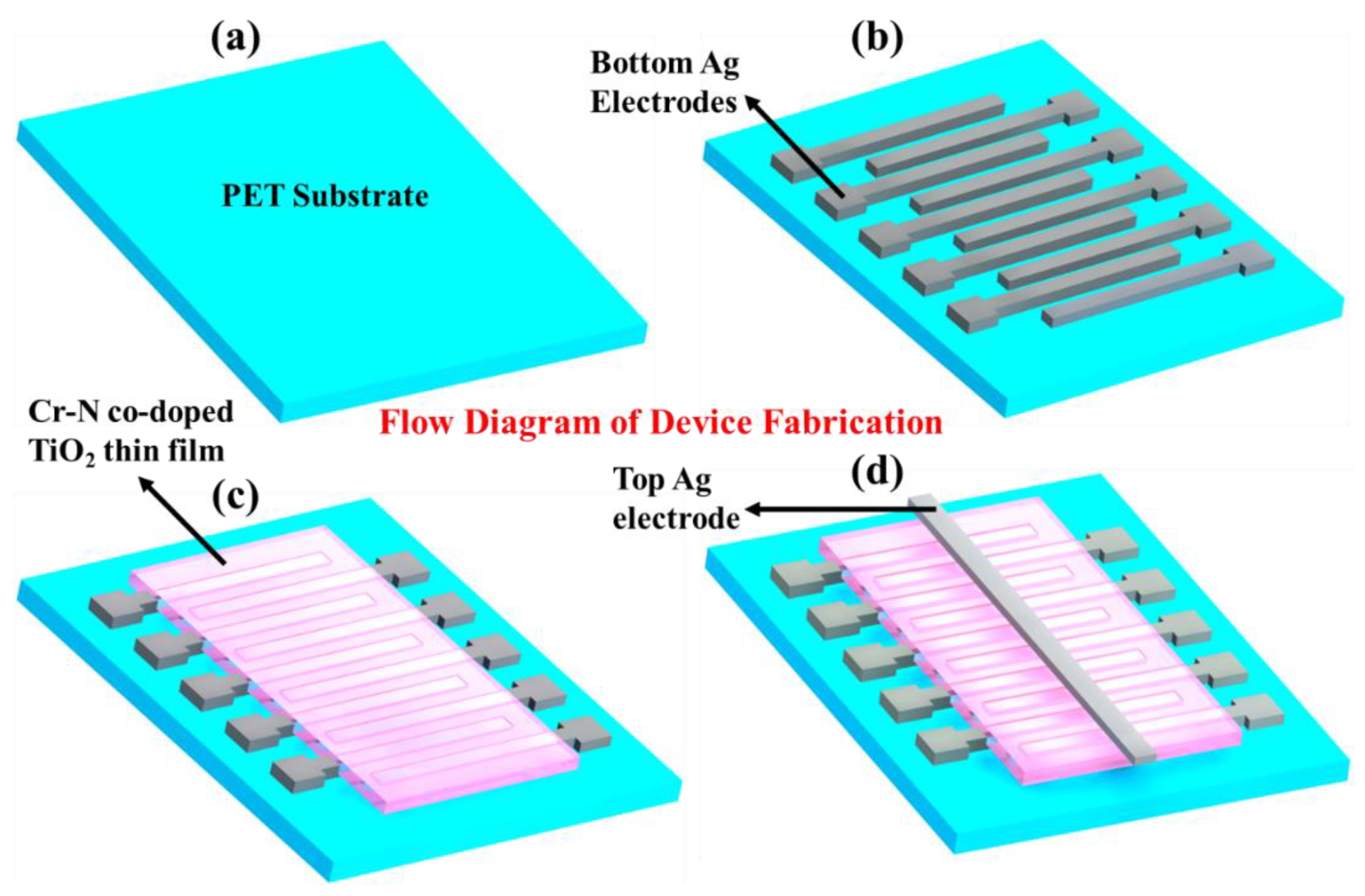
Abstract
:1. Introduction
2. Experimental Section
2.1. Materials
2.2. Synthesis of Cr-N Doped TiO2 NPs
2.3. Memristor Fabrication
2.4. Characterization
3. Results and Discussion
3.1. Characterization of Cr-N Doped TiO2 NPs
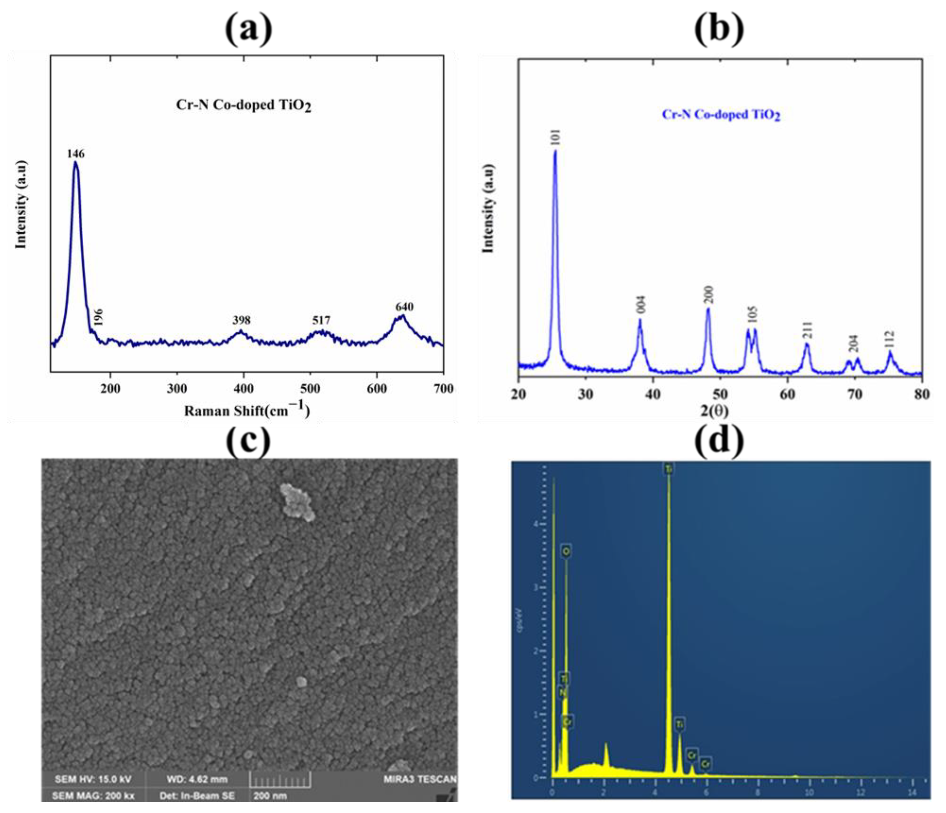
3.1.1. Raman Analysis
3.1.2. XRD Analysis
3.1.3. FESEM Analysis
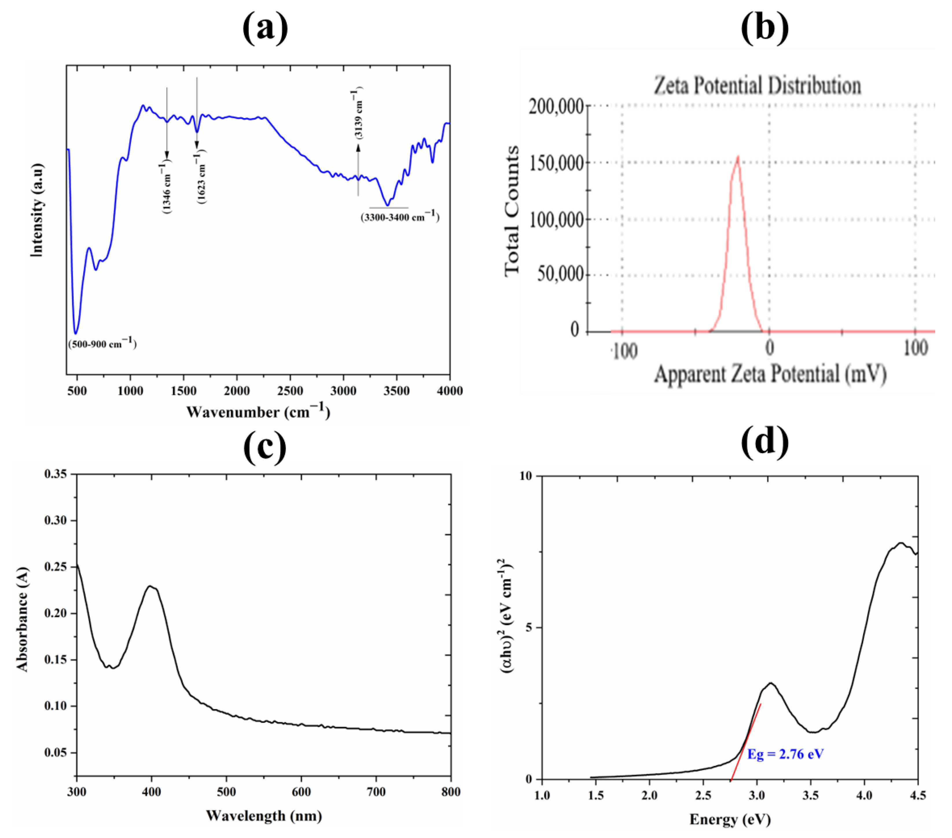
3.1.4. FTIR Analysis
3.1.5. Zeta Potential Analysis
3.1.6. UV-Vis Analysis
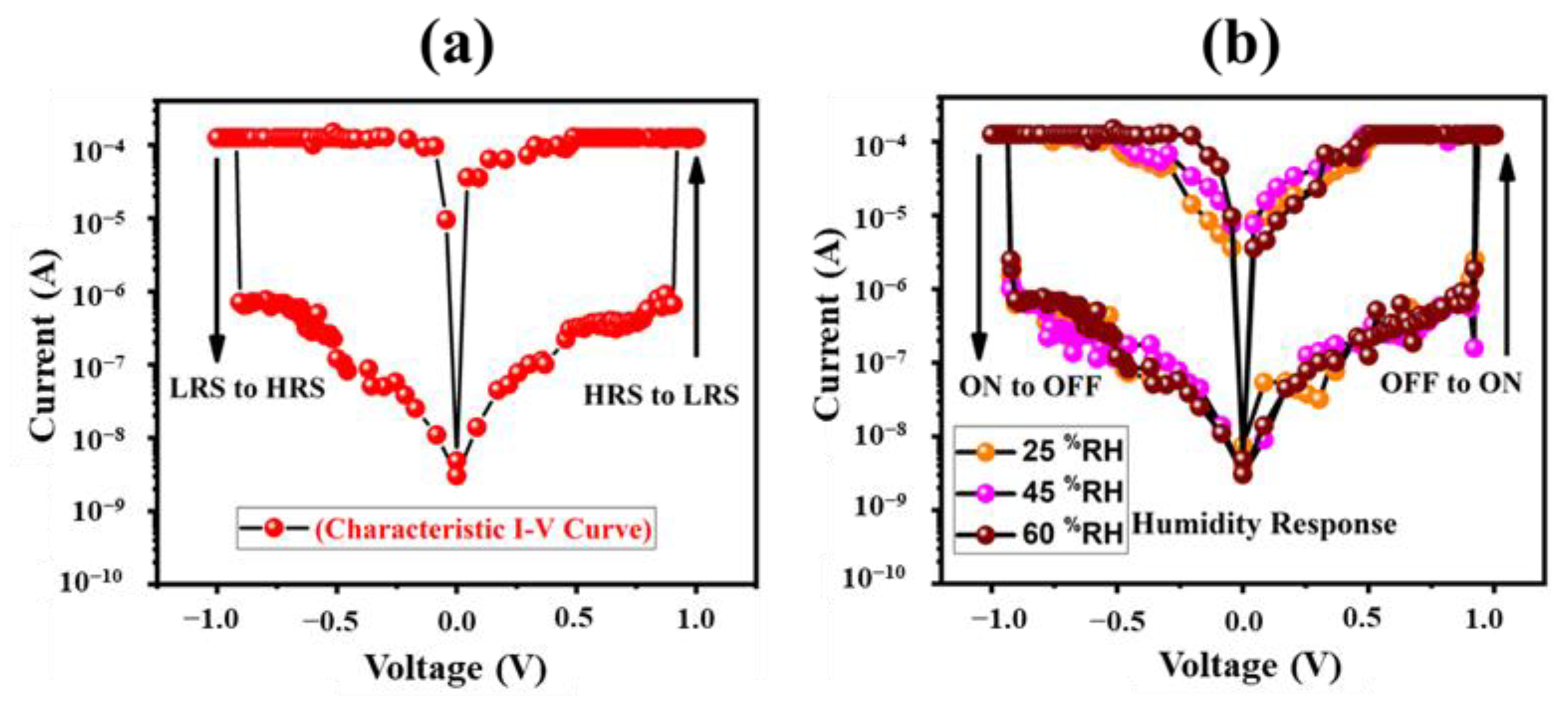
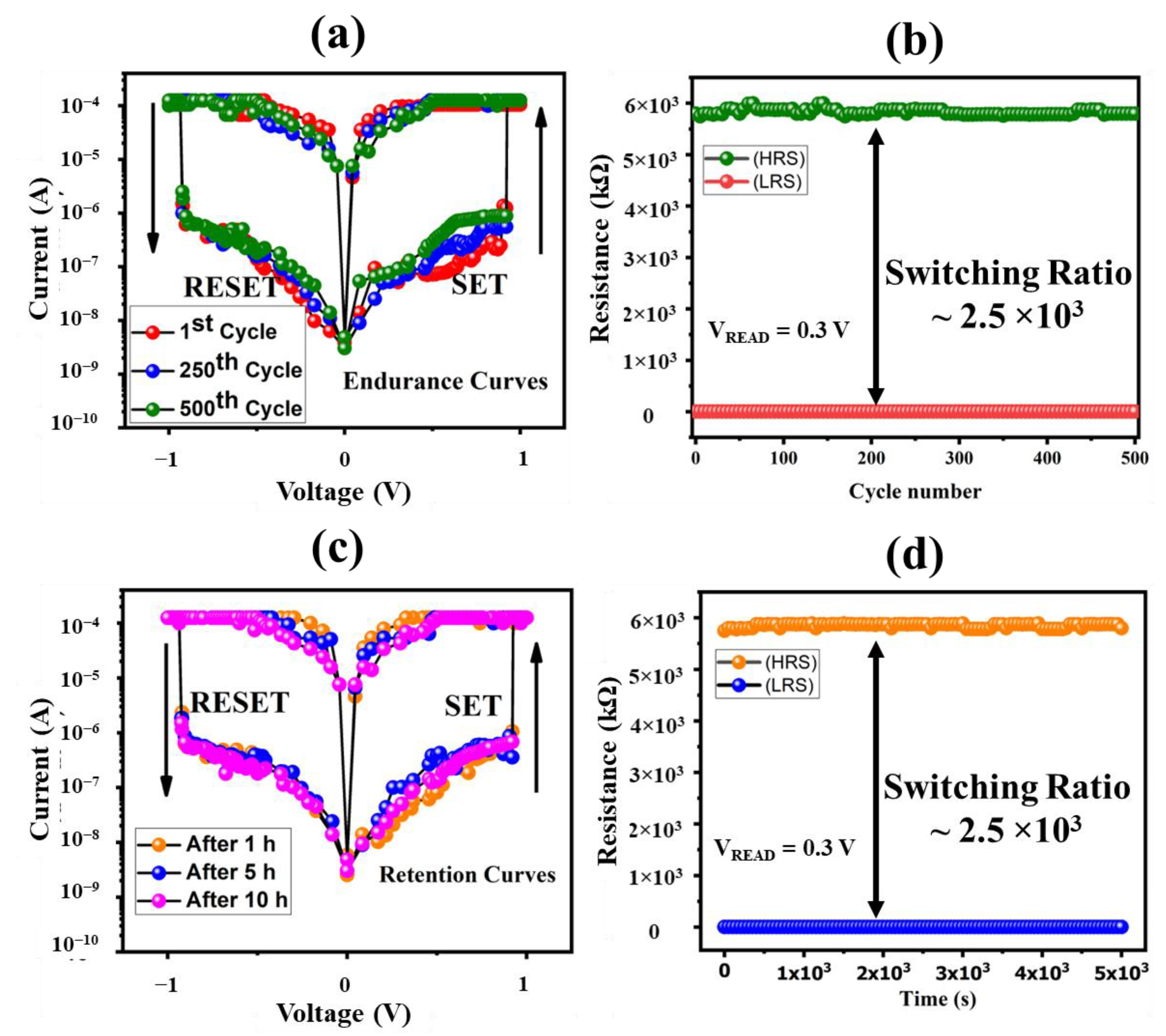
3.2. Electrical Characterization
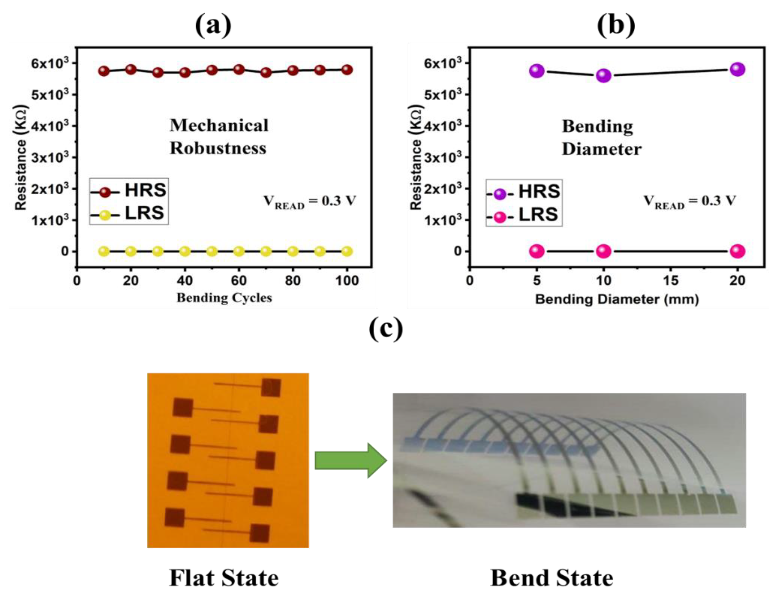
3.3. Mechanical Characterization
4. Conclusions
Author Contributions
Funding
Institutional Review Board Statement
Informed Consent Statement
Data Availability Statement
Conflicts of Interest
References
- Rehman, M.M.; Rehman, H.M.M.U.; Gul, J.Z.; Kim, W.Y.; Karimov, K.S.; Ahmed, N. Decade of 2D-materials-based RRAM devices: A review. Sci. Technol. Adv. Mater. 2020, 21, 147–186. [Google Scholar] [CrossRef] [Green Version]
- Yang, J.J.; Strukov, D.B.; Stewart, D.R. Memristive devices for computing. Nat. Nanotechnol. 2013, 8, 13–24. [Google Scholar] [CrossRef] [PubMed]
- Caravelli, F.; Carbajal, J. Memristors for the Curious Outsiders. Technologies 2018, 6, 118. [Google Scholar] [CrossRef] [Green Version]
- Wang, W.; Song, W.; Yao, P.; Li, Y.; van Nostrand, J.; Qiu, Q.; Ielmini, D.; Yang, J.J. Integration and Co-Design of Memristive Devices and Algorithms for Artificial Intelligence. IScience 2020, 23, 101809. [Google Scholar] [CrossRef] [PubMed]
- Nugent, M.A.; Molter, T.W. Thermodynamic-RAM technology stack. Int. J. Parallel Emergent Distrib. Syst. 2018, 33, 430–444. [Google Scholar] [CrossRef] [Green Version]
- Berdan, R.; Vasilaki, E.; Khiat, A.; Indiveri, G.; Serb, A.; Prodromakis, T. Emulating short-term synaptic dynamics with memristive devices. Sci. Rep. 2016, 6, 18639. [Google Scholar] [CrossRef] [PubMed] [Green Version]
- Indiveri, G.; Linares-Barranco, B.; Legenstein, R.; Deligeorgis, G.; Prodromakis, T. Integration of nanoscale memristor synapses in neuromorphic computing architectures. Nanotechnology 2013, 24, 384010. [Google Scholar] [CrossRef] [Green Version]
- Chakrabarti, B.; Lastras-Montaño, M.A.; Adam, G.; Prezioso, M.; Hoskins, B.; Payvand, M.; Madhavan, A.; Ghofrani, A.; Theogarajan, L.; Cheng, K.-T.; et al. A multiply-add engine with monolithically integrated 3D memristor crossbar/CMOS hybrid circuit. Sci. Rep. 2017, 7, 42429. [Google Scholar] [CrossRef] [Green Version]
- Ielmini, D.; Pedretti, G. Device and Circuit Architectures for In-Memory Computing. Adv. Intell. Syst. 2020, 2, 2000040. [Google Scholar] [CrossRef]
- Du, C.; Cai, F.; Zidan, M.A.; Ma, W.; Lee, S.H.; Lu, W.D. Reservoir computing using dynamic memristors for temporal information processing. Nat. Commun. 2017, 8, 2204. [Google Scholar] [CrossRef]
- Hus, S.M.; Ge, R.; Chen, P.-A.; Liang, L.; Donnelly, G.E.; Ko, W.; Huang, F.; Chiang, M.-H.; Li, A.-P.; Akinwande, D. Observation of single-defect memristor in an MoS2 atomic sheet. Nat. Nanotechnol. 2021, 16, 58–62. [Google Scholar] [CrossRef] [PubMed]
- Siddiqui, G.U.; Rehman, M.M.; Yang, Y.-J.; Choi, K.H. A two-dimensional hexagonal boron nitride/polymer nanocomposite for flexible resistive switching devices. J. Mater. Chem. C 2017, 5, 862–871. [Google Scholar] [CrossRef]
- Zhou, G.; Sun, B.; Hu, X.; Sun, L.; Zou, Z.; Xiao, B.; Qiu, W.; Wu, B.; Li, J.; Han, J.; et al. Negative Photoconductance Effect: An Extension Function of the TiOx-Based Memristor. Adv. Sci. 2021, 8, 2003765. [Google Scholar] [CrossRef]
- Spagnolo, M.; Morris, J.; Piacentini, S.; Antesberger, M.; Massa, F.; Crespi, A.; Ceccarelli, F.; Osellame, R.; Walther, P. Experimental photonic quantum memristor. Nat. Photonics 2022, 16, 318–323. [Google Scholar] [CrossRef]
- Wang, Y.; Gong, Y.; Yang, L.; Xiong, Z.; Lv, Z.; Xing, X.; Zhou, Y.; Zhang, B.; Su, C.; Liao, Q.; et al. MXene-ZnO Memristor for Multimodal in-Sensor Computing. Adv. Funct. Mater. 2021, 31, 2100144. [Google Scholar] [CrossRef]
- Rehman, M.M.; ur Rehman, H.M.M.; Kim, W.Y.; Sherazi, S.S.H.; Rao, M.W.; Khan, M.; Muhammad, Z. Biomaterial-Based Nonvolatile Resistive Memory Devices toward Ecofriendliness and Biocompatibility. ACS Appl. Electron. Mater. 2021, 3, 2832–2861. [Google Scholar] [CrossRef]
- Wu, L.; Liu, H.; Li, J.; Wang, S.; Wang, X. A Multi-level Memristor Based on Al-Doped HfO2 Thin Film. Nanoscale Res. Lett. 2019, 14, 177. [Google Scholar] [CrossRef] [Green Version]
- Athanasiou, V.; Konkoli, Z. On using reservoir computing for sensing applications: Exploring environment-sensitive memristor networks. Int. J. Parallel Emergent Distrib. Syst. 2018, 33, 367–386. [Google Scholar] [CrossRef]
- Cavallini, M.; Hemmatian, Z.; Riminucci, A.; Prezioso, M.; Morandi, V.; Murgia, M. Regenerable Resistive Switching in Silicon Oxide Based Nanojunctions. Adv. Mater. 2012, 24, 1197–1201. [Google Scholar] [CrossRef]
- Closson, A.; Richards, H.; Xu, Z.; Jin, C.; Dong, L.; Zhang, J.X.J. Method for Inkjet-Printing PEDOT: PSS Polymer Electrode Arrays on Piezoelectric PVDF-TrFE Fibers. IEEE Sens. J. 2021, 21, 26277–26285. [Google Scholar] [CrossRef]
- Wen, D.; Wang, X.; Liu, L.; Hu, C.; Sun, C.; Wu, Y.; Zhao, Y.; Zhang, J.; Liu, X.; Ying, G. Inkjet Printing Transparent and Conductive MXene (Ti3C2Tx) Films: A Strategy for Flexible Energy Storage Devices. ACS Appl. Mater. Interfaces 2021, 13, 17766–17780. [Google Scholar] [CrossRef] [PubMed]
- Rehman, M.M.; Siddiqui, G.U.; Doh, Y.H.; Choi, K.H. Highly flexible and electroforming free resistive switching behavior of tungsten disulfide flakes fabricated through advanced printing technology. Semicond. Sci. Technol. 2017, 32, 095001. [Google Scholar] [CrossRef]
- Li, S.; Pam, M.; Li, Y.; Chen, L.; Chien, Y.; Fong, X.; Chi, D.; Ang, K. Wafer-Scale 2D Hafnium Diselenide Based Memristor Crossbar Array for Energy-Efficient Neural Network Hardware. Adv. Mater. 2021, 34, 2103376. [Google Scholar] [CrossRef] [PubMed]
- Sherazi, S.S.H.; Rehman, M.M.; Ur Rehman, H.M.M.; Kim, W.Y.; Siddiqui, G.U.; Karimov, K.S. Electroforming-free flexible organic resistive random access memory based on a nanocomposite of poly(3-hexylthiophene-2,5-diyl) and orange dye with a low threshold voltage. Semicond. Sci. Technol. 2020, 35, 125012. [Google Scholar] [CrossRef]
- Rehman, M.M.; Yang, B.-S.; Yang, Y.-J.; Karimov, K.S.; Choi, K.H. Effect of device structure on the resistive switching characteristics of organic polymers fabricated through all printed technology. Curr. Appl. Phys. 2017, 17, 533–540. [Google Scholar] [CrossRef]
- Kim, S.; Jung, S.; Kim, M.-H.; Chen, Y.-C.; Chang, Y.-F.; Ryoo, K.-C.; Cho, S.; Lee, J.-H.; Park, B.-G. Scaling Effect on Silicon Nitride Memristor with Highly Doped Si Substrate. Small 2018, 14, 1704062. [Google Scholar] [CrossRef]
- Sokolov, A.S.; Ali, M.; Riaz, R.; Abbas, Y.; Ko, M.J.; Choi, C. Silver-Adapted Diffusive Memristor Based on Organic Nitrogen-Doped Graphene Oxide Quantum Dots (N-GOQDs) for Artificial Biosynapse Applications. Adv. Funct. Mater. 2019, 29, 1807504. [Google Scholar] [CrossRef]
- Zhu, Y.-L.; Xue, K.-H.; Cheng, X.-M.; Qiao, C.; Yuan, J.-H.; Li, L.-H.; Miao, X.-S. Uniform and robust TiN/HfO2/Pt memristor through interfacial Al-doping engineering. Appl. Surf. Sci. 2021, 550, 149274. [Google Scholar] [CrossRef]
- Liu, Y.; Ye, C.; Chang, K.; Li, L.; Jiang, B.; Xia, C.; Liu, L.; Zhang, X.; Liu, X.; Xia, T.; et al. A Robust and Low-Power Bismuth Doped Tin Oxide Memristor Derived from Coaxial Conductive Filaments. Small 2020, 16, 2004619. [Google Scholar] [CrossRef]
- Yan, X.; Zhao, J.; Liu, S.; Zhou, Z.; Liu, Q.; Chen, J.; Liu, X.Y. Memristor with Ag-Cluster-Doped TiO2 Films as Artificial Synapse for Neuroinspired Computing. Adv. Funct. Mater. 2018, 28, 1705320. [Google Scholar] [CrossRef]
- Yuan, F.; Li, S.; Deng, Y.; Li, Y.; Chen, G.R. Cu-doped TiO2-x nanoscale memristive applications in chaotic circuit and true random number generator. IEEE Trans. Ind. Electron. 2022, 0046, 1. [Google Scholar] [CrossRef]
- Kim, S.; Lee, J.; Ling, L.; Liu, S.E.; Lim, H.; Sangwan, V.K.; Hersam, M.C.; Lee, H. Sodium-Doped Titania Self-Rectifying Memristors for Crossbar Array Neuromorphic Architectures. Adv. Mater. 2022, 34, 2106913. [Google Scholar] [CrossRef] [PubMed]
- Yu, Y.; Wang, C.; Jiang, C.; Wang, L.; Wang, Z.; Du, Z.; Sun, J.; Abrahams, I.; Huang, X. Nitrogen-doped titanium dioxide nanorod array memristors with synaptic features and tunable memory lifetime for neuromorphic computing. J. Alloys Compd. 2021, 868, 159194. [Google Scholar] [CrossRef]
- Rehman, M.M.; Siddiqui, G.U.; Gul, J.Z.; Kim, S.-W.; Lim, J.H.; Choi, K.H. Resistive Switching in All-Printed, Flexible and Hybrid MoS2-PVA Nanocomposite based Memristive Device Fabricated by Reverse Offset. Sci. Rep. 2016, 6, 36195. [Google Scholar] [CrossRef] [PubMed] [Green Version]
- Khalid, M.A.U.; Kim, S.W.; Lee, J.; Soomro, A.M.; Rehman, M.M.; Lee, B.-G.; Choi, K.H. Resistive switching device based on SrTiO3/PVA hybrid composite thin film as active layer. Polymer 2020, 189, 122183. [Google Scholar] [CrossRef]
- Kernazhitsky, L.; Shymanovska, V.; Gavrilko, T.; Naumov, V.; Fedorenko, L.; Kshnyakin, V.; Baran, J. Photoluminescence of Cr-doped TiO2 induced by intense UV laser excitation. J. Lumin. 2015, 166, 253–258. [Google Scholar] [CrossRef]
- Nasir, M.; Bagwasi, S.; Jiao, Y.; Chen, F.; Tian, B.; Zhang, J. Characterization and activity of the Ce and N co-doped TiO2 prepared through hydrothermal method. Chem. Eng. J. 2014, 236, 388–397. [Google Scholar] [CrossRef]
- Bsiri, N.; Zrir, M.A.; Bardaoui, A.; Bouaїcha, M. Morphological, structural and ellipsometric investigations of Cr doped TiO2 thin films prepared by sol–gel and spin coating. Ceram. Int. 2016, 42, 10599–10607. [Google Scholar] [CrossRef]
- Zhao, Z.; Omer, A.A.; Qin, Z.; Osman, S.; Xia, L.; Singh, R.P. Cu/N-codoped TiO2 prepared by the sol-gel method for phenanthrene removal under visible light irradiation. Environ. Sci. Pollut. Res. 2020, 27, 17530–17540. [Google Scholar] [CrossRef]
- Dette, C.; Pérez-Osorio, M.A.; Kley, C.S.; Punke, P.; Patrick, C.E.; Jacobson, P.; Giustino, F.; Jung, S.J.; Kern, K. TiO2 Anatase with a Bandgap in the Visible Region. Nano Lett. 2014, 14, 6533–6538. [Google Scholar] [CrossRef]
- Karim, S.; Ahmad, N.; Hussain, D.; Mok, Y.S.; Siddiqui, G.U. Active removal of anionic azo dyes (MO, CR, EBT) from aqueous solution by potential adsorptive capacity of zinc oxide quantum dots. J. Chem. Technol. Biotechnol. 2022. [Google Scholar] [CrossRef]


Publisher’s Note: MDPI stays neutral with regard to jurisdictional claims in published maps and institutional affiliations. |
© 2022 by the authors. Licensee MDPI, Basel, Switzerland. This article is an open access article distributed under the terms and conditions of the Creative Commons Attribution (CC BY) license (https://creativecommons.org/licenses/by/4.0/).
Share and Cite
Khan, M.; Mutee Ur Rehman, H.M.; Tehreem, R.; Saqib, M.; Rehman, M.M.; Kim, W.-Y. All-Printed Flexible Memristor with Metal–Non-Metal-Doped TiO2 Nanoparticle Thin Films. Nanomaterials 2022, 12, 2289. https://doi.org/10.3390/nano12132289
Khan M, Mutee Ur Rehman HM, Tehreem R, Saqib M, Rehman MM, Kim W-Y. All-Printed Flexible Memristor with Metal–Non-Metal-Doped TiO2 Nanoparticle Thin Films. Nanomaterials. 2022; 12(13):2289. https://doi.org/10.3390/nano12132289
Chicago/Turabian StyleKhan, Maryam, Hafiz Mohammad Mutee Ur Rehman, Rida Tehreem, Muhammad Saqib, Muhammad Muqeet Rehman, and Woo-Young Kim. 2022. "All-Printed Flexible Memristor with Metal–Non-Metal-Doped TiO2 Nanoparticle Thin Films" Nanomaterials 12, no. 13: 2289. https://doi.org/10.3390/nano12132289