Article

Spin-Orbit Coupling Electronic Structures of Organic-Group Functionalized Sb and Bi Topological Monolayers

School of Material Science and Chemical Engineering, Harbin University of Science and Technology, Harbin 150040, China
*
Author to whom correspondence should be addressed.
Nanomaterials 2022, 12(12), 2041; https://doi.org/10.3390/nano12122041
Submission received: 12 May 2022 / Revised: 2 June 2022 / Accepted: 10 June 2022 / Published: 14 June 2022
(This article belongs to the Special Issue Computational Study of Nanomaterials)

Abstract

:
Electronic band-gap is a key factor in applying two-dimensional (2D) topological insulators into room-temperature quantum spin Hall effect (QSH) spintronic devices. Employing pseudopotential plane-wave first-principles calculations, we investigate spin-orbit coupling (SOC) electronic structures of the novel 2D topological insulator series of antimony (Sb) and bismuth (Bi) monolayers (isolated double atomic layers) functionalized by organic-groups (methyl, amino and hydroxyl). Cohesive energies and phonon frequency dispersion spectra indicate that these organic-group decorated Sb and Bi monolayers possess structural stability in both energetic statics and lattice dynamics. The giant electronic band-gaps adequate for room-temperature applications are attributed to the effective SOC enhancement of group functionalization. The nontrivial topology of these novel 2D monolayer materials is verified by the Z2 invariant derived from wave-function parity and edge-states of their nanoribbons, which is prospective for QSH spintronic devices. The chemical functional group changes the p-orbital component of Fermi level electrons, leading to strong intra-layer spin-orbit coupling, opening a large band-gap of approaching 1.4 eV at Dirac-cone point and resulting in a global indirect band-gap of 0.75 eV, which, even underestimated, is adequate for room-temperature operations. Sb and Bi monolayers functionalized by organic groups are also predicted to maintain stable nontrivial topology under in-layer biaxial strain, which is suitable for epitaxy technology to realize QSH spintronic devices.

1. Introduction

Two-dimensional (2D) topological insulator (TI) with quantum spin Hall effect is a new class of topological quantum state matter whose electronic structure presents intrinsic time-inversion-symmetry (Z2 conservation) of nontrivial topology, which means its physical properties and quantum-states are not affected by material defects or impurities and will provide a potential application platform for energy-free spintronic devices [1,2]. Conductive surfaces or edge-states of Z2 conserved topological insulators are restrained by spin-time inversion symmetry, and the electron motions of macroscopic conduction currents rely on the electron spin states [3,4]. In 2D TI materials, electrons are not subjected to back scattering from nonmagnetic impurities, and therefore the energy loss of Joule heat will not be generated during edge-state electron transports [5]. Because the spin-orbit coupling (SOC) of carbon atoms is very weak, the Dirac-cone band-gap of graphene under SOC is only on the order of 10−3 meV, far from realizing 2D TI applications of room-temperature spintronic devices [6]. Graphane-like silicene, germanene, chemically modified sitene and the compound ZeTe5 have also been theoretically proven to be 2D TI materials. So far, only HgTe/CdTe and InAs/GaSb quantum wells have been experimentally demonstrated to be 2D TI materials with a very small bulk band-gap, which, however, can only fulfill QSH at very low temperatures and fail to be applied in room-temperature electronic devices [7,8,9,10]. Therefore, the development of a new class of 2D TI materials with adequately wide electronic band-gaps is the prerequisite for energy-free spintronic devices, which is of great significance to the collective scientific knowledge of topological quantum states.
Serrated hexagonal honeycomb 2D materials composed of antimony (Sb) or bismuth (Bi) elements have strong SOC, which are expected to become a new class of room-temperature 2D TI [11,12]. It has been proven by first-principles calculations that Sb (111) film will be transformed into 2D topological phase under planar biaxial strain, while Bi (111) film (hereinafter referred to as monolayer) is a 2D TI with a bulk band-gap of about 0.2 eV [13,14]. Although the Bi monolayer was prepared experimentally, its QSH has not been observed until now [15,16]. 2D topological materials with a large band-gap can be obtained through halination and hydrogenation, but the plasma method of experimental preparation leads to a sharp increase in lattice defects and even a serious impact on topological properties, making it difficult to achieve high-quality chemical modifications [17]. In contrast, the functionalization reactions of organic groups are relatively slow and more suitable to increase bulk band-gaps by passivating the surface conjugate bonds of 2D materials [18]. BiX (B, Al, Ga, and In) compound monolayers have been predicted by first-principles calculations to be capable of acquiring substantial improvements in their bulk band-gaps by surface hydrogenation, which even results in energy band inversions of their nanoribbons [19]. Whereas a hydrogenated surface is easily oxidized at room temperature and normal pressure due to its poor chemical stability, while the functionalized surface of organic groups has antioxidant capability and higher thermal stability for successful device applications [20,21,22]. Therefore, the chemical modifications of Sb and Bi monolayers by organic groups are preferable for realizing 2D topological materials with giant band-gaps.
In this paper, the electronic structures and topological properties of methyl, amino, and hydroxyl functionalized Sb and Bi monolayers are calculated by the first-principles pseudopotential plane-wave method. We focus on electronic band-gap, band-edge splitting, and atomic orbital components under SOC, investigating the effect of organic-group functionalizations on the electronic band-gaps and nontrivial topology of Sb and Bi monolayers according to the Z2 invariant and topological edge-states, exploring their potential applications in QSH electronics. The influence of in-plane biaxial strain on band-gap and topological properties are also elucidated to prove that the organic-group functionalized Sb and Bi monolayers have mechanical stability for nontrivial topology and giant band-gaps to withstand electron thermal excitations at room temperature.

2. Atomic Model and Calculation Schemes

Atomic structures and electronic properties of Sb and Bi monolayers functionalized with organic groups are calculated by first-principles pseudopotential plane-wave schemes, as implemented by CASTEP code of Material Studio 2020 package (Accelrys Inc., Materials Studio version 2020.08, San Diego, CA, USA). Gradient correction exchange-correlation functional PBESOL is adopted to calculate SOC-included electronic-states [23]. To reveal the SOC-produced energetic splitting of electronic-states with different spin components, the band structures without SOC are also calculated in comparison to the SOC-included band structures. The interaction of valence electrons with atomic-cores is described by norm-conserving pseudopotential, and the relativistic effect is evaluated by Koelling–Harmon treatment [24]. Electronic wave-functions are expanded by the plane-wave basis-set with a cutoff kinetic energy of 900 eV. The energy and stress are calculated under finite basis-set correction to adequately reduce the calculation error of basis-set finiteness [25]. Self-consistent field iteration in convergence of 5 × 10⁻⁷ eV/atom is performed by Pulay schemes of density mixing with a charge mixing amplitude of 0.5, in which electron density is calculated on a high-resolution FFT grid of 40 × 40 × 216 [26,27]. The k-point sampling of Brillouin zone integration is carried out on Monkhorst-Pack 5 × 5 × 1 grid [28]. Atomic-structure relaxation is achieved by geometrical optimization of energy functional minimization using LBFGS algorithm to obtain energy convergence of 5.0 × 10⁶ eV/atom so that atomic interaction force and internal stress are less than 0.01 eV/Å and 0.02 GPa, respectively [29]. Phonon structure (phonon frequency dispersion spectrum) is calculated by the linear response method [30], in which the convergence standard of mechanical constant is set as 1.0 × 10⁻⁵ eV/Å2, and the non-analytical correction is applied to calculate the frequency-splitting of longitudinal-transverse optical phonons at G point.

3. Results and Discussion

3.1. Atomic Structure

Atomic structures of Sb and Bi monolayers with chemical decorations of methyl, amino, and hydroxyl functional groups (SbXHn and BiXHn: XHn = CH3, NH2, OH) are shown in Figure 1 where the high-symmetric dispersion paths in Brillouin zone are also exhibited. The p-orbitals of Sb and Bi atoms are in sp3 hybridization with methyl, amino, or hydroxyl groups bonded to the unsaturated pz-orbitals of Sb or Bi atoms on the surfaces of monolayers. The 2D crystal structures of SbXHn and BiXHn incorporate two Sb or Bi bonding atoms and two identical chemical groups into one primitive unit-cell of trigonal point group D3d or monoclinic C2h, with a space symmetry group of P-3M1 or C2/M.
Space symmetry groups, lattice constants, cohesive energies, bond lengths, warping thicknesses of Sb or Bi atomic-layers, and total monolayer thicknesses of SbXHn and BiXHn in geometry-optimized structures are listed in Table 1. Cohesive energies are calculated by formula Ecoh = 2(Em + Egroup) − Eunit, where Em, Egroup and Eunit denote total energies of the isolated Sb or Bi atoms, the chemical groups, and the primitive unit-cells of SbXHn or BiXHn, respectively. The cohesive energies of SbXHn and BiXHn approach 13~16 eV/unitcell, which is overall higher than that of TMD and III-VI compound monolayers [31,32,33], implying their energetic stability in statics.
Kinetic stabilities of SbXHn and BiXHn are evaluated by the phonon dispersion spectra of their relaxed atomic structures (after geometrical optimization), as shown in Figure 2. Their phonon dispersion curves are comprised of 9 branches, including 3 acoustic branches and 6 optical branches. Three kinds of acoustic phonon modes are longitudinal waves, in-plane transverse waves, and off-plane transverse waves (from high frequency to low). The six optical branches contain two sets of optical waves, each incorporating a non-degenerate off-plane transverse mode and a pair of G-point degenerate longitudinal and in-plane transverse modes. Neither SbXHn nor BiXHn represent any virtual frequencies, i.e., all the intrinsic frequencies of phonon modes are positive, demonstrating that they are kinetically stable two-dimensional structures.

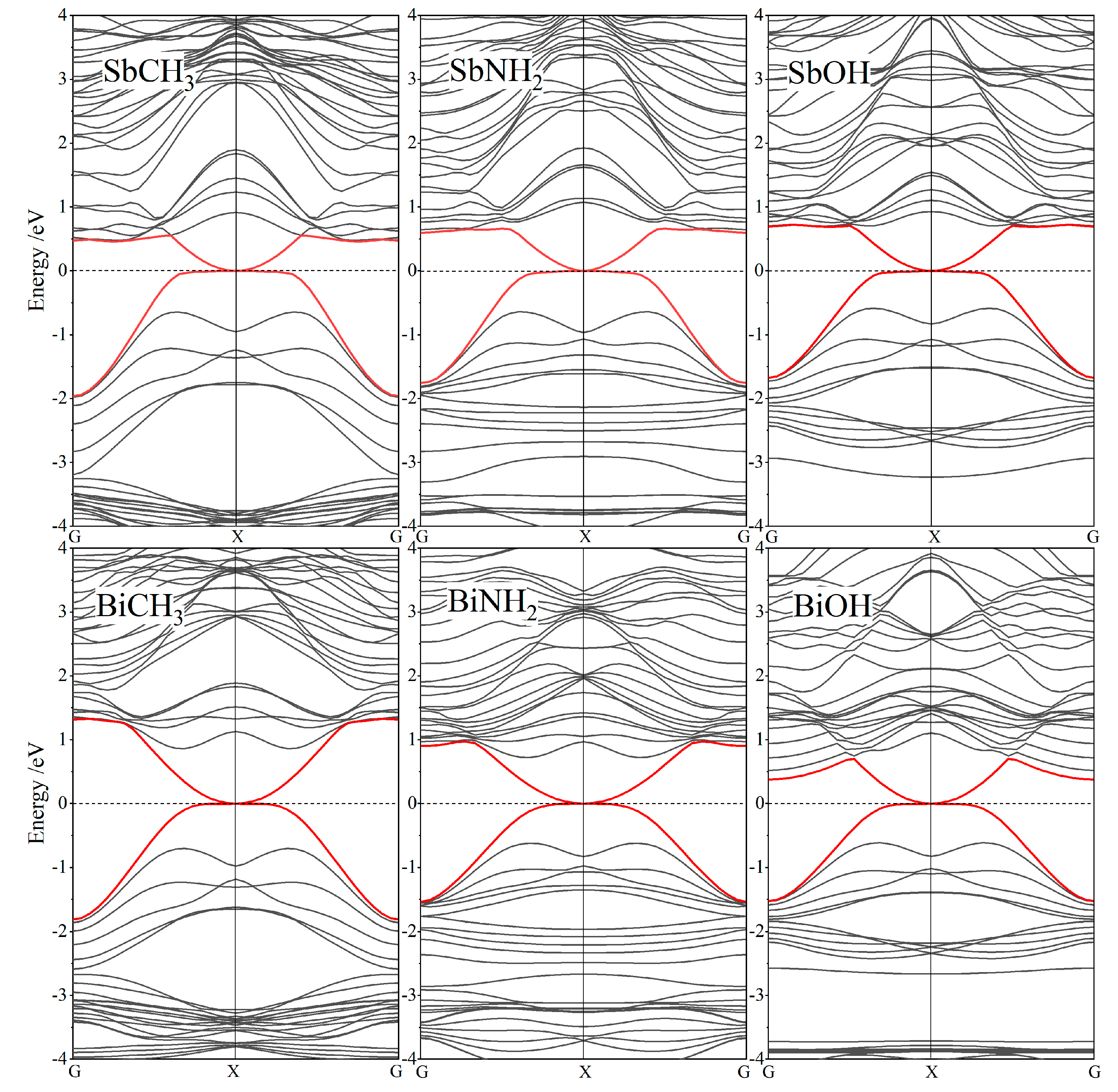
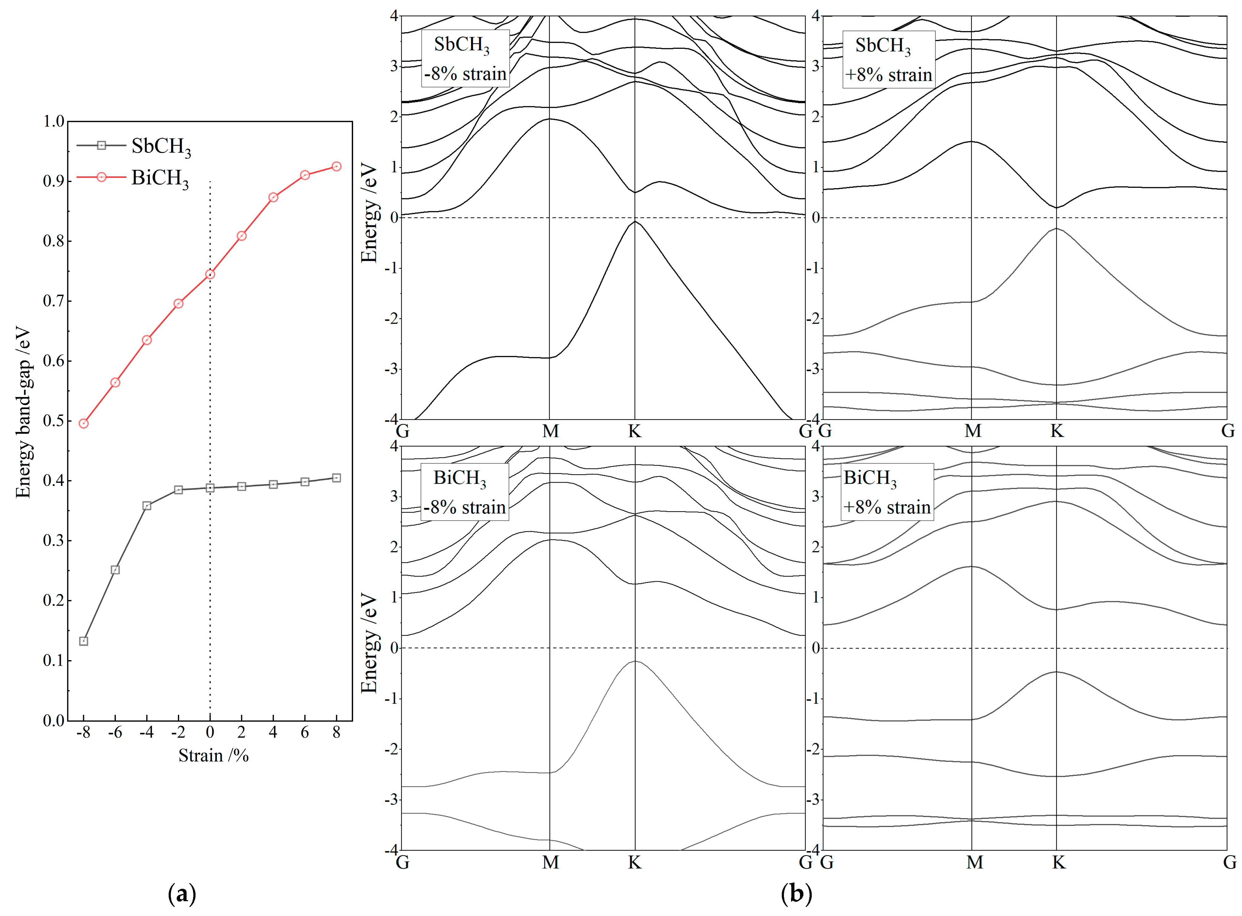
3.2. Band Structure and Topological Property

In the absence of SOC, the methyl or hydroxyl modified Sb and Bi monolayers represent a metallic band structure, with the lowest conduction and highest valence bands crossing on Fermi level at K point, as shown by red curves in Figure 3. For SbXHn and BiXHn, the linear energy-k dispersion (constant first derivative) at band-edges characterizes the typical Dirac-cone point, similar to graphene and halogenated Bi monolayers, but the orbital compositions of electronic-states at Dirac-cone point are significantly discrepant from that of pure Bi monolayer. Moreover, without SOC, Dirac-cone points of SbNH2 and BiNH2 show band inversions, forming band-gaps of 0.112 eV and 0.050 eV, respectively. There are two (even) bonded hydrogen atoms on one amine group, which leads to C2h point-symmetry of SbNH2 and BiNH2, indicating that a pair of degenerate electronic-states at high symmetry points in band structures will split into two energy levels; that is, two crossing energy dispersion curves at high symmetry points will split into two energy bands of upper and lower concave. Therefore, in the absence of SOC, degenerate states of Dirac-cone point at K point undergo energy level splitting to open a non-degenerate band-gap, in which the resulted band-edge electronic-states have mixed components of conduction and valence bands, accounting for energy band inversions.
SOC determines band structures near Fermi levels of SbXHn and BiXHn, which splits the degenerate energy levels of conduction and valence bands at Dirac-cone point to form significant band-gaps. Therefore, by including SOC, the SbXHn and BiXHn represent as the direct and indirect band-gap semiconductors, respectively, as shown by black curves in Figure 3. This SOC-introduced feature is similar to 2D TI monolayers of silene, germanene, and ZeTe5, while SbXHn and BiXHn give rise to giant bulk band-gaps (the highest value approaching 0.745 eV as shown in Table 2) remarkably larger than ~0.2 eV of pure Bi monolayer, which means a more preferable stability for realizing exotic quantum effects such as QSH at room temperature. Since the GGA functional always underestimates DFT band-gaps generally by about 40% [34], the real band-gaps of SbXHn and BiXHn will somehow be higher than the calculated values reported in this paper. Even underestimated, the predicted giant bulk band-gaps (>0.3 eV) can still adequately impede electron thermal-excitation at room temperature, indicating the feasible realizations of topological electronic devices by SbXHn and BiXHn.
The obvious deformation of Dirac-cone under SOC indicates the presence of a topologically nontrivial phase where the giant band-gaps also originates from SOC, implying that SbXHn and BiXHn are likely nontrivial topological insulators, but still requiring TI characteristics of band structure represented by Z2 invariant and edge-states. Eigenvalues (topological index) ν = 1 and ν = 0 of Z2 topological invariant characterize the nontrivial topological phase (topological insulator) and the trivial topological phase (normal insulator), respectively. Accordingly, the topological properties of SbXHn and BiXHn are analyzed to determine whether they are topologically nontrivial. Since the atomic structures of SbXHn and BiXHn possess space inversion symmetry, their Z2 topological invariants can be calculated directly from the parities of Bloch wave-functions of the occupied electronic-states at all the time-reversal-invariant points (TRIP). Electronic structures of SbXHn and BiXHn have four TRIP, one at G point and three at M point, so the topological index P can be calculated as follows:
P ( K i ) = m = 1 N δ 2 m i , ( 1 ) ν = i = 1 4 P ( K i ) = P ( G ) P ( M ) 3
where P denotes the parity product of Bloch wave-functions on TRIP, δ = ±1 indicates parity, and N is the number of valence bands. The 24 valence electrons in primitive unit-cell of SbXHn or BiXHn constitute 12 spin-degenerate levels at TRIP, and the parities of spin-degenerate electron eigen-functions of SbXHn and BiXHn on TRIP are identical. As shown in Table 3, the values of P at G and M points are −1 and +1, respectively, which leads to a nontrivial topological invariant of Z2 = 1, demonstrating that SbXHn and BiXHn are nontrivial topological insulators.
Nontrivial topological properties of SbXHn and BiXHn should, meanwhile, be manifested by the odd number of conductive channels from zero band-gap edge-states, where Dirac-cone points connecting conduction and valence bands at Fermi level should appear in band structures of their nanoribbons. The zigzag nanoribbons of SbXHn and BiXHn are modeled with a mirror-symmetry around ribbon center axis and the edge unsaturated bonds being hydrogenated. The nanoribbon width is specified approaching ~30 Å to prohibit overlapping of electronic wave-functions between two nanoribbon edges. After geometrical optimizations, the band structures of SbXHn and BiXHn nanoribbons are calculated, with the results being shown in Figure 4.
Energy dispersion curves of nanoribbon edge-states intersect through the Dirac-cone point on Fermi level at the boundary X point of one-dimensional Brillouin zone. The odd number of edge-state conductive channels derived from the nontrivial topology will also present edge-state Dirac-cones in band structures of SbXHn and BiXHn arm-chair nanoribbons. To this end, these Dirac-cones of edge states demonstrate that SbXHn and BiXHn are nontrivial topological insulators which are supported by their giant-band-gaps to realize QSH effect at room temperature.
Although the SOC strengths of organic groups used for chemical modifications on Sb and Bi monolayers are almost negligible, the resulted band-gaps caused by SOC are significantly increased. For example, the bulk band-gap of pure Bi monolayer is only 0.2 eV, while the SOC band-gap is increased to 0.745 eV by methyl functionalization. Both the pure Sb or Bi monolayer and SbXHn or BiXHn (XHn≠NH2) possess p-orbital components of electronic-states near Fermi level that could be distinguished into pz and px/y where the SOC intensity of px/y-orbitals is much higher than that of pz-orbitals. The Fermi-level electronic-states of Sb or Bi monolayer are mainly derived from pz-orbitals of Sb or Bi atoms (similar to graphene and silene), while Fermi-level orbital components of SbXHn or BiXHn originates dominantly from px/y-orbitals of Sb or Bi atoms. Chemical decorations of organic groups (functionalization) eliminate the delocalized conjugate π bonds of Sb or Bi pz-orbitals near Fermi level and produce the localized σ bonds below Fermi level by the functionalized groups. Therefore, the Fermi-level electronic-states of SbXHn and BiXHn are dominated by px/y-orbital components, accounting for the evident enhancement of SOC to acquire giant bulk band-gaps.
Chemical modifications of organic groups result in a significant increase in lattice constants of Sb and Bi monolayers, as shown in Table 1. The band-gap improvement under planar biaxial tension is due to that SOC strength increases with the bonding distance between Sb or Bi atoms. Thus, the increment of lattice constant or bonding distance of strong SOC atoms by chemical functionalizations of organic groups is another important attribute to the large band-gaps of SbXHn and BiXHn. Compared to Sb and Bi monolayers, the lattice constants of SbXHn and BiXHn exceed by 30%, while their giant band-gaps and nontrivial topological properties do not change significantly with a strain below ±8%. SbXHn and BiXHn retain their nontrivial topology under biaxial strains approaching ±8%, and their band-gaps decrease by less than 10% under biaxial strains below ±4%, as shown in Figure 5. Tensile and compressive strains cause, respectively, the rise and fall of a conduction band minimum at G point with respect to Fermi level. As a result, the tensile strain evidently bears on the band-gaps of BiXHn with indirect band structures, but not on the direct band-gaps of SbXHn. In contrast, after the compressive strain increases to −4%, the direct band-gaps of SbXHn alternate to indirect band-gaps, and thus their global band-gap varies more intensively with compressive strain than that of BiXHn. The giant band-gap and nontrivial topology of SbXHn and BiXHn are quite stable in regards to mechanical deformations, indicating they are robust in broad mechanical and thermal conditions for experimental tests and spintronic device applications.

4. Conclusions

Electronic structures and topological properties of Sb and Bi monolayers functionalized with organic groups (SbXHn and BiXHn, X = C, N, O) are studied by first-principles calculations in the consideration of SOC. Cohesive energies and phonon dispersion spectra indicate that these monolayered systems are innate of both statically and kinetically stable in atomic structures. Topologically nontrivial band-structures and nanoribbon edge-states prove that SbXHn and BiXHn are intrinsic two-dimensional topological insulators with the largest bulk band-gap approaching 0.75 eV. Due to the much higher SOC strength of px/y orbitals of Sb and Bi atoms than that of pz-orbitals, the organic group modifications of Sb and Bi monolayers make the dominant p-orbital component at Fermi level alter from pz to px/y, which results in a significant increase in their electronic band-gaps. Z2 topological invariant and Dirac-cone edge-states consistently demonstrate the nontrivial topology of SbXHn and BiXHn. In-plane biaxial strains being increased to ±8% leads to no significant change in bulk band-gap, under which the topologically nontrivial properties of SbXHn and BiXHn still remain. Stable two-dimensional topological insulators with giant electronic band-gaps are predicted to be achieved by functionalizing Sb and Bi monolayers with organic groups, which provides a theoretical basis and strategy for developing novel quantum topological materials. The present study suggests SbXHn and BiXHn are valuable of great scientific interest and prospective of potential applications in topological electronic devices.

Author Contributions

Data curation, formal analysis, writing—original draft preparation, writing—review and editing, Q.G.; conceptualization, investigation, project administration, G.Z. All authors have read and agreed to the published version of the manuscript.

Funding

This research was funded by the National Natural Science Foundation of China (Grant No. 51973046).

Institutional Review Board Statement

Not applicable.

Informed Consent Statement

Not applicable.

Data Availability Statement

Theoretical methods and results are available from all the authors.

Conflicts of Interest

The authors declare no conflict of interest.

References

  1. Bernevig, B.A.; Hughes, T.L.; Zhang, S.C. Quantum spin Hall effect and topological phase transition in HgTe quantum wells. Science 2006, 314, 1757–1761. [Google Scholar] [CrossRef] [PubMed] [Green Version]
  2. König, M.; Wiedmann, S.; Brüne, C.; Roth, A.; Buhmann, H.; Molenkamp, L.W.; Qi, X.L.; Zhang, S.C. Quantum spin Hall insulator state in HgTe quantum wells. Science 2007, 318, 766–770. [Google Scholar] [CrossRef] [PubMed] [Green Version]
  3. Rasche, B.; Isaeva, A.; Ruck, M.; Borisenko, S.; Zabolotnyy, V.; Büchner, B.; Koepernik, K.; Ortix, C.; Richtern, M.; van den Brink, J. Stacked topological insulator built from bismuth-based graphene sheet analogues. Nat. Mater. 2013, 12, 422–425. [Google Scholar] [CrossRef] [PubMed]
  4. Moore, J.E. The birth of topological insulators. Nature 2013, 464, 194–198. [Google Scholar] [CrossRef]
  5. Bernevig, B.A.; Zhang, S.C. Quantum spin Hall effect. Phys. Rev. Lett. 2006, 96, 106802. [Google Scholar] [CrossRef] [Green Version]
  6. Kane, C.L.; Mele, E.J. Quantum spin Hall effect in graphene. Phys. Rev. Lett. 2005, 95, 226801. [Google Scholar] [CrossRef] [Green Version]
  7. Chuang, F.C.; Hsu, C.H.; Chen, C.Y.; Huang, Z.Q.; Ozolins, V.; Lin, H.; Bansil, A. Tunable topological electronic structures in Sb (111) bilayers: A first-principles study. Appl. Phys. Lett. 2013, 102, 22424. [Google Scholar] [CrossRef]
  8. Xu, Y.; Yan, B.H.; Zhang, H.J.; Wang, J.; Xu, G.; Tang, P.; Duan, W.H.; Zhang, S.C. Large-gap quantum spin Hall insulators in tin films. Phys. Rev. Lett. 2013, 111, 136804. [Google Scholar] [CrossRef]
  9. Weng, H.M.; Dai, X.; Fang, Z. Transition-metal pentatelluride ZrTe5 and HfTe5: A paradigm for large-gap quantum spin Hall insulators. Phys. Rev. X 2014, 4, 11002. [Google Scholar]
  10. Si, C.; Liu, J.W.; Xu, Y.; Wu, J.; Gu, B.L.; Duan, W.H. Functionalized germanene as a prototype of large-gap two-dimensional topological insulators. Phys. Rev. B 2014, 89, 115429. [Google Scholar] [CrossRef] [Green Version]
  11. Zhang, P.F.; Liu, Z.; Duan, W.; Liu, F.; Wu, J. Topological and electronic transitions in a Sb(111) nanofilm: The interplay between quantum confinement and surface effect. Phys. Rev. B 2013, 85, 201410. [Google Scholar] [CrossRef] [Green Version]
  12. Huang, Z.Q.; Chuang, F.C.; Hsu, C.H.; Liu, Y.T.; Chang, H.R.; Lin, H.; Bansil, A. Nontrivial topological electronic structures in a single Bi(111) bilayer on different substrates: A first-principles study. Phys. Rev. B 2013, 88, 165301. [Google Scholar] [CrossRef]
  13. Wada, M.; Murakami, S.; Freimuth, F.; Bihlmayer, G. Localized edge states in two-dimensional topological insulators: Ultrathin Bi films. Phys. Rev. B 2011, 83, 121310. [Google Scholar] [CrossRef] [Green Version]
  14. Liu, Z.; Liu, C.X.; Wu, Y.S.; Duan, W.H.; Liu, F.; Wu, J. Stable nontrivial Z2 topology in ultrathin Bi(111) films: A first-principles study. Phys. Rev. Lett. 2011, 107, 136805. [Google Scholar] [CrossRef] [Green Version]
  15. Yang, F.; Miao, L.; Wang, Z.F.; Yao, M.Y.; Zhu, F.; Song, Y.R.; Wang, M.X.; Xu, J.P.; Fedorov, A.V.; Sun, Z.; et al. Spatial and energy distribution of topological edge states in single Bi(111) bilayer. Phys. Rev. Lett. 2012, 109, 16801. [Google Scholar] [CrossRef] [Green Version]
  16. Wang, Z.F.; Yao, M.Y.; Ming, W.; Miao, L.; Zhu, F.; Liu, C.; Gao, C.L.; Qian, D.; Jia, J.F.; Liu, F. Creation of helical Dirac fermions by interfacing two gapped systems of ordinary fermions. Nat. Commun. 2013, 4, 1384. [Google Scholar] [CrossRef] [Green Version]
  17. Wu, J.; Xie, L.M.; Li, Y.; Wang, H.; Ouyang, Y.; Guo, J.; Dai, H.G. Controlled chlorine plasma reaction for noninvasive graphene doping. J. Am. Chem. Soc. 2011, 133, 19668–19671. [Google Scholar] [CrossRef]
  18. Jiang, S.S.; Butler, S.; Bianco, E.; Restrepo, O.D.; Windl, W.; Goldberger, J.E. Improving the stability and optical properties of germanane via one-step covalent methyl-termination. Nat. Commun. 2014, 5, 3389. [Google Scholar] [CrossRef]
  19. Freitas, R.R.Q.; Rivelino, R.; de Brito Mota, F.; de Castilho, M.C. Topological insulating phases in two-dimensional bismuth containing single layers preserved by hydrogenation. J. Phys. Chem. C 2015, 119, 23599–23606. [Google Scholar] [CrossRef] [Green Version]
  20. Becerril, H.A.; Mao, J.; Liu, Z.; Stoltenberg, R.M.; Bao, Z.; Chen, Y. Evaluation of solution-processed reduced graphene oxide films as transparent conductors. ACS Nano 2008, 2, 463–470. [Google Scholar] [CrossRef]
  21. Knapp, D.; Brunschwig, B.S.; Lewis, N.S. Chemical, electronic, and electrical properties of alkylated Ge(111) surfaces. J. Phys. Chem. C 2010, 114, 12300–12307. [Google Scholar] [CrossRef] [Green Version]
  22. Ma, Y.D.; Dai, Y.; Kou, L.Z.; Frauenheim, T.; Heine, T. Robust two-dimensional topological insulators in methylfunctionalized bismuth, antimony, and lead bilayer films. Nano Lett. 2015, 15, 1083–1089. [Google Scholar] [CrossRef] [PubMed]
  23. Perdew, J.P.; Ruzsinszky, A.; Csonka, G.I.; Vydrov, O.A.; Burke, K. Restoring the Density-Gradient Expansion for Exchange in Solids and Surfaces. Phys. Rev. Lett. 2008, 100, 136406. [Google Scholar] [CrossRef] [PubMed] [Green Version]
  24. Lin, J.S.; Qteish, A.; Payne, M.C.; Heine, V. Optimized and transferable nonlocal separable ab initio pseudopotentials. Phys. Rev. B 1993, 47, 4174–4180. [Google Scholar] [CrossRef]
  25. Milman, V.; Lee, M.H.; Payne, M.C. Ground-state properties of CoSi2 determined by a total-energy pseudopotential method. Phys. Rev. B 1994, 49, 16300–16308. [Google Scholar] [CrossRef]
  26. Payne, M.C.; Teter, M.P.; Allan, D.C.; Arias, T.A.; Joannopoulos, J.D. Iterative minimization techniques for ab initio total energy calculations: Molecular dynamics and conjugate gradients. Rev. Mod. Phys. 1992, 64, 1045–1097. [Google Scholar] [CrossRef] [Green Version]
  27. Kresse, G.; Furthmuller, J. Efficient iterative schemes for ab initio total-energy calculations using a plane-wave basis set. Phys. Rev. B 1996, 54, 11169–11186. [Google Scholar] [CrossRef]
  28. Monkhorst, H.J.; Pack, J.D. Special points for Brillouin-zone integrations—A reply. Phys. Rev. B 1977, 16, 1748. [Google Scholar]
  29. Packwood, D.; Kermode, J.; Mones, L.; Bernstein, N.; Woolley, J.; Gould, N.; Ortner, C.; Csanyi, G. A universal pre-conditioner for simulating condensed phase materials. J. Chem. Phys. 2016, 144, 164109. [Google Scholar] [CrossRef] [Green Version]
  30. Baroni, S.; de Gironcoli, S.; dal Corso, A.; Giannozzi, P. Phonons and related crystal properties from density-functional perturbation theory. Rev. Mod. Phys. 2001, 73, 515–562. [Google Scholar] [CrossRef] [Green Version]
  31. Wang, N.; Cao, D.; Wang, J.; Liang, P.; Chen, X.; Shu, H. Semiconducting edges and flake-shape evolution of monolayer GaSe: Role of edge reconstructions. Nanoscale 2018, 10, 12133–12140. [Google Scholar] [CrossRef] [PubMed]
  32. Guo, Y.; Zhou, S.; Bai, Y.; Zhao, J. Enhanced piezoelectric effect in Janus group-III chalcogenide monolayers. Appl. Phys. Lett. 2017, 110, 163102. [Google Scholar] [CrossRef]
  33. Xu, X.D.; Sun, W.F. First-principles investigation of GaInSe2 monolayer as a janus material. J. Chin. Ceram. Soc. 2020, 48, 507–513. [Google Scholar]
  34. Borlido, P.; Schmidt, J.; Huran, A.W.; Tran, F.; Marques, M.A.L.; Botti, S. Exchange-correlation functionals for band gaps of solids: Benchmark, reparametrization and machine learning. npj Comput. Mater. 2020, 6, 96. [Google Scholar] [CrossRef]
Figure 1. (ac) Schematics of SbXHn and BiXHn monolayers decorated with methyl, amino, and hydroxyl groups, respectively, in which violet, gray, blue, red, and white balls symbolize the bonding atoms of Sb/Bi, carbon, nitrogen, oxygen, and hydrogen, respectively; (d) high symmetry points in the dispersion paths of electronic energy and phonon frequency in Brillouin zone.
Nanomaterials 12 02041 g001
Figure 2. Phonon frequency dispersion spectra of SbXHn and BiXHn in atom-relaxed structures.
Nanomaterials 12 02041 g002
Figure 3. Band structures of SbXHn and BiXHn with SOC (black curves) and without SOC (red curves), in reference to Fermi level (horizontal dash lines).
Nanomaterials 12 02041 g003
Figure 4. The SOC-incorporated band structures of SbXHn (top panels) and BiXHn (bottom panels) zigzag nanoribbons in reference to Fermi level as energy zero (horizontal dash lines).
Nanomaterials 12 02041 g004
Figure 5. (a) Global bulk band-gaps in dependence on bi-axial strains of −8~8% and (b) band structures under ±8% bi-axial strains for SbCH3 and BiCH3, which are calculated with SOC included.
Nanomaterials 12 02041 g005
Table 1. Space symmetry, lattice constants a, chemical bonding lengths (dMM and dMX: M = Sb, Bi; X = C, N, O), thicknesses of the internal Sb/Bi layer and the entire monolayer (vertical distances between two Sb/Bi atomic-planes hm and between the outermost two hydrogen atomic-planes on two surface sides ht), and cohesive energy (Ecoh) of SbXHn and BiXHn compared to Sb and Bi monolayers.
MonolayersSpace SymmetryadMMdMXhmhtEcoh/(eV·unitcell−1)
SbP6/MMM4.7442.7398.728
SbCH3P-3M15.0202.8982.0990.0585.00514.367
SbNH2C2/M4.9652.8941.9550.0174.98415.293
SbOHP-3M15.0162.8961.7690.0445.48516.232
BiP6/MMM4.9602.8647.998
BiCH3P-3M15.3093.0662.2250.0675.24412.943
BiNH2C2/M5.4553.1842.1340.4795.54713.520
BiOHP-3M15.2893.0591.9170.1735.92814.501
Table 2. The SOC-introduced Dirac-cone splitting-gaps at K point ED(K) and the resulted indirect band-gaps from K point to G point Eg(G-K) of SbXHn and BiXHn.
MonolayersED (K)Eg (G-K)MonolayersED K)Eg (G-K)
SbCH30.388-BiCH31.3120.745
SbNH20.370-BiNH21.3960.498
SbOH0.311-BiOH1.3480.309
Table 3. Parities δ and their product P of spin-degenerate states at TRIP for SbXHn and BiXHn.
TRIPParity δP
G+1+1+1−1−1−1+1+1−1+1−1+1−1
3 M+1−1−1+1+1−1−1+1+1−1+1−1+1
Publisher’s Note: MDPI stays neutral with regard to jurisdictional claims in published maps and institutional affiliations.

