Article

Investigation of Heater Structures for Thermal Conductivity Measurements of SiO2 and Al2O3 Thin Films Using the 3-Omega Method

1
Department of Electrical Engineering and Media Technology, Deggendorf Institute of Technology, Dieter-Görlitz-Platz 1, 94469 Deggendorf, Germany
2
Faculty of Electrical Engineering and Information Technology, University of the Bundeswehr Munich, Werner-Heisenberg-Weg 39, 85577 Neubiberg, Germany
3
Department of Electrical Engineering, Helmut Schmidt University/University of the Federal Armed Forces Hamburg, Holstenhofweg 85, 22043 Hamburg, Germany
4
Department of Applied Physics, University of Barcelona, Martí i Franquès 1, 08028 Barcelona, Spain
5
Infineon Technologies AG, Wernerwerkstraße 2, 93049 Regensburg, Germany
6
Chair of Electronic Devices, RWTH Aachen University, Otto-Blumenthal-Straße 2, 52074 Aachen, Germany
*
Author to whom correspondence should be addressed.
Nanomaterials 2022, 12(11), 1928; https://doi.org/10.3390/nano12111928
Submission received: 26 April 2022 / Revised: 27 May 2022 / Accepted: 1 June 2022 / Published: 4 June 2022

Abstract

:
A well-known method for measuring thermal conductivity is the 3-Omega (3ω) method. A prerequisite for it is the deposition of a metal heater on top of the sample surface. The known design rules for the heater geometry, however, are not yet sufficient. In this work, heaters with different lengths and widths within the known restrictions were investigated. The measurements were carried out on SiO2 thin films with different film thicknesses as a reference. There was a significant difference between theoretical deposited heater width and real heater width, which could lead to errors of up to 50% for the determined thermal conductivity. Heaters with lengths between 11 and 13 mm and widths of 6.5 µm or more proved to deliver the most trustworthy results. To verify the performance of these newfound heaters, additional investigations on Al2O3 thin films were carried out, proving our conclusions to be correct and delivering thermal conductivity values of 0.81 Wm−1 K−1 and 0.93 Wm−1 K−1 for unannealed and annealed samples, respectively. Furthermore, the effect of annealing on Al2O3 was studied, revealing a significant shrinking in film thickness of approximately 11% and an increase in thermal conductivity of 15%. The presented results on well-defined geometries will help to produce optimized heater structures for the 3ω method.

Graphical Abstract

1. Introduction

Measuring the thermal conductivity of thin films is of great importance, as these films are vital components within semiconductor devices and integrated circuits [1,2]. Zhao et al. and others [3,4] alluded that the properties of thin films may vary significantly from those of their bulk material counterparts. Therefore, separate investigation is crucial. To this end, various measurement methods may be deployed. Among them are thermoreflectance imaging [5,6], the time-domain thermoreflectance method (TDTR) [7,8], the laser flash method [9,10], the micro-Raman method [11,12], scanning thermal microscopy (SThM) [13,14], and many more.
The 3ω method is one of those methods and is commonly used to measure cross-plane thermal conductivity. It was first introduced by O. Corbino in 1910 to measure the thermal diffusivity of a metal filament in light bulbs [15,16]. In 1987, Birge and Nagel investigated the frequency-dependent specific heat of liquids using an immersed thin planar heater [17]. Cahill et al. used a heater deposited on top of dielectric solids in order to measure thermal conductivity for the first time in 1989 [18]. In 1997, Lee et al. adapted the method for thin film measurements down to a thickness of 20 nm [19]. Two years later, in-plane and cross-plane thermal conductivities of anisotropic materials were measured [20,21]. Since 2006, the 3ω method has been adapted to many different samples, such as carbon nanotubes [22], gases [23], and free-standing membranes [24].
In this work, a closer look was taken at the heater structure, which is required to perform 3ω measurements. It is commonly known that the heater width has to be much larger than the film thickness to measure true cross-plane thermal conductivity. Furthermore, the heater has to be considered infinitely long. These and other requirements have been defined by others and are briefly explained later. Although these requirements exist, there are two major problems:
  • Because of the imprecise specifications of heater geometries, researchers define their structures individually [19,22,25,26,27]. This leads to inaccuracies and a large spread of measurement results.
  • Even if all requirements are fulfilled, choosing different heater geometries within the boundaries still leads to differing results.
To fix these problems, a comprehensive study of a wide range of heater geometries was performed. The goal thereof was to provide recommendations on valid heater geometries, which should simplify the choice of the right 3ω layouts for other researchers. Therefore, first, measurements with different heater structures were performed on well-known SiO2 thin films. In a second step, the best heater geometries were tested on Al2O3 thin films as a verification process.

2. Materials and Methods

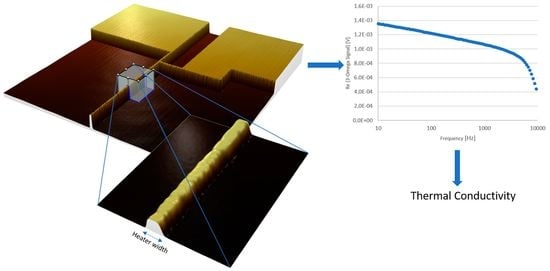
2.1. Three-Omega Method

The 3ω method, as used today, was first introduced by Cahill et al. in 1990 [28] and is widely used to measure thermal properties of bulk and thin film materials [29,30,31]. For the application of the 3ω method, a metal heater, as can be seen in Figure 1, has to be deposited on top of the sample.
The 3ω method has a fast thermal response time, which allows for quick measurements; it is robust against convection and radiation losses; and it is insensitive against the boundary condition between substrate and environment [32]. To measure electrically conducting films, an electrically isolating layer between the heater and the film is needed [3].
A current with frequency 1ω flows through the heater, which is heated by joule heating as a consequence. The temperature and resistance of said heater change with frequency 2ω, and the voltage over the heater oscillates with frequency 3ω. This 3ω component contains information about the temperature amplitude of the heater, which is used to calculate the thermal conductivity of the material of interest [33]. However, since this 3ω component is quite small, a Wheatstone bridge and a lock-in amplifier (Anfatec eLock-In 204/2, Oelsnitz, Germany) are utilized to ensure reliable detection. The bridge circuit is illustrated in Figure 1. The measurement is performed for frequencies between 10 Hz and 10 kHz.
To heat the sample, an AC current with frequency ω is sent through the heater. This current I(t) can be expressed by [3]:
I ( t ) = I 0 × cos ( ω t ) ,
where I0 is the current amplitude. The dissipated heating power P(t) can be written as:
P ( t ) = I ( t ) 2 × R h = I 0 2 × R h 2 × ( 1 + cos ( 2 ω t ) ) ,
with Rh as the electrical resistance of the heater. The dissipated power P(t) can be rewritten as [34]:
P ( t ) = P D C + P 2 ω × cos ( 2 ω t ) ,
where PDC is the DC component and Pcos × (2ωt) is the AC component of the dissipated power. The power oscillates with frequency 2ω, and so does the temperature change over time of the heater ∆T(t). This can be written as [3]:
Δ T ( t ) = Δ T 2 ω × cos ( 2 ω t + φ ) ,
where ∆T2ω is the temperature change amplitude, which contains the thermal conductivity information, and φ is the phase shift introduced because of the inertia of Joule heating [3]. As described by the temperature coefficient of resistance α R :
α R = 1 R h , 0 × d R h ( T ) d T ,
where Rh,0 is the resistance of the heater at a reference temperature, the resistance of said heater changes with its temperature. Therefore, the resistance is time-dependent, which can be seen from Equation (4). This resistance change can be expressed as [3]:
R h ( t ) = R h , o × ( 1 + α R × Δ T 2 ω × cos ( 2 ω t + φ ) ) .
In this experiment, the voltage drop over the metal heater was measured. Therefore, an expression for this voltage had to be found, which was done by multiplying Equations (1) and (6):
U ( T ) = I ( t ) · R h ( t )
U ( t ) = R h , 0 × I 0 × cos ( ω t ) + R h , 0 × I 0 × α R × Δ T 2 ω 2 × cos ( ω t + φ ) + R h , 0 × I 0 × α R × Δ T 2 ω 2 × cos ( 3 ω t + φ )
U ( t ) = U 0 × cos ( ω t ) + U 0 × α R × Δ T 2 ω 2 × cos ( ω t + φ ) + U 0 × α R × Δ T 2 ω 2 × cos ( 3 ω t + φ ) ,
information is contained in ∆T2ω, and therefore the 3ω component of U(t), is of great interest. Since the 3ω signal is a few magnitudes smaller than the 1ω signal [28,32], a lock-in amplifier (LIA) and a bridge circuit are used to detect the 3ω signal. From Equation (9), we receive:
Δ T 2 ω = 2 α R × U 3 ω , r m s U 0 , r m s
with respect to the 3ω component only. Approximating the first harmonic voltage response as the input voltage signal, Equation (10) can be rewritten as:
Δ T 2 ω = 2 α R × U 3 ω , r m s U ω , r m s .
The temperature change amplitude ∆T2ω can be rewritten as:
Δ T 2 ω = Δ T s + Δ T f .
where ∆Ts and ∆Tf are the temperature change amplitudes of the bulk and the thin film. The LIA detects the bridge voltage W3ω. Therefore, the 3ω voltage drop over the heater has to be calculated by [25]:
U 3 ω , r m s = R v + R s R v × W 3 ω .
The temperature change amplitude of the bulk ∆Ts can be calculated using [19]:
Δ T s = P l × π × k s × [ 1 2 × l n ( k s c × p × b 2 ) + η 1 2 × l n ( 2 ω ) ] ,
where η was experimentally determined to be 1.05, according to Lee and Cahill [19], and c and p are the specific heat capacity and the density of the substrate, respectively.
To obtain the temperature change amplitude of the thin film ∆Tf, only ∆Ts has to be subtracted from ∆T2ω:
Δ T f = Δ T 2 ω Δ T s .
The thermal conductivity of the thin film kf can finally be calculated by [3,27]:
k f = P × d f 2 b × l × Δ T f ,
where df is the thin film thickness. It should be noted that there are a variety of other ways of evaluating 3ω measurements. For more detailed information about other approaches, see [20,27,34,35,36].

2.2. Prerequisites for the 3-Omega Method

The following approximations are prerequisites for the theory explained above or were determined by simulations or experimental results [27,28,32,37,38,39]. By fulfilling all of those requirements, the valid heater geometries and measurement frequencies are defined, achieving a theoretical error of less than 1%. All approximations can be seen in Table 1, where λ = D / ω is the thermal wavelength, D is the thermal diffusivity, h is the heat transfer coefficient for convection and radiation, and the indices x and z describe the anisotropy in the in-plane and cross-plane directions, respectively [27,28,32,37,38,39]. The last requirement shown in Table 1 can be mostly neglected, and if it is, the resulting error is still below 3% even for values > 4.8 [32].

2.3. Investigations on Heater Dimensions Using Laser Scanning Microscopy

In this work, a laser scanning microscope (LSM; Zeiss LSM 800, Oberkochen, Germany) was used to measure both the length and width of the heater with great precision. This was mandatory, as both parameters do have a significant influence on the result. The length of each heater was measured using an optical stitching method integrated into the LSMs’ ZEN-Software, enabling high-resolution images at large scales.
Because of the deposition process, the heaters did not have perfect rectangular cross-sections, as can be seen in Figure 2. Thus, it was necessary to measure the width at the contact area, which is not possible with a normal optical microscope. Therefore, a z-scan using the built-in laser, featuring a wavelength of 405 nm, was performed, which delivered a high-resolution 3D image of the heater. An example is shown in Figure 2. The deviation from the theoretical deposited value to the real measured value was typically around 2 µm, which would lead to a thermal conductivity error of 20–50% depending on the heater width.

2.4. Materials

2.4.1. Silicon Dioxide

Silicon dioxide (SiO2) thin films are widely used in micro- and nanoelectronics and semiconductor devices [40]. The main field of application for SiO2 is as a gate oxide in said semiconductor devices, for example, MOS structures. Because of its very well-known manufacturing methods, it is also used in a variety of other applications, such as separating individual chips from each other in integrated circuits or optical technologies [40]. In this work, SiO2 was taken as a reference, since its thermal conductivity for film thicknesses even below 100 nm is well known. These reference values are presented in Table 2. The samples used in this work were cut from eight-inch silicon wafers (GlobalWafers Co., Ltd., Hsinchu, Taiwan) with a thickness of 730 µm. They exhibited SiO2 thin films with thicknesses of 107 nm, 510 nm, and 1018 nm deposited on top using plasma-enhanced chemical vapor deposition (PECVD) with a deposition temperature of 400 °C.

2.4.2. Aluminum Oxide

All Al2O3 thin films investigated in this work were manufactured using atomic layer deposition (ALD) (Infineon Technologies AG, Regensburg, Germany). Depending on the process temperature, the ALD Al2O3 thin film was usually amorphous after deposition [39,45,46]. Aarik et al. used different process temperatures ranging from 200 to 760 °C and found that crystalline films of 110 nm thickness could be manufactured using process temperatures exceeding 600 °C [45]. The finished sample could then be annealed, allowing the amorphous material to form crystals and become fully crystalline as long as the right parameters were chosen. Jakschik et al. investigated 3 to 8 nm thin films and found crystallization for temperatures above 900–1000 °C [47], while Zhang et al. found crystallization temperatures of 1050–1150 °C for a film thickness of 47 nm [39]. Additionally, temperatures over 1200 °C seem to destroy the crystalline structure [39]. It must be noted that Jakschik used 60–1800 s as process time, while Zhang used only 90 s [39,47]. With lower process temperature, longer process duration is needed for crystallization [47], while in general higher temperatures yield better crystallization results [39]. With high annealing temperatures, the density of the material increases, while the film thickness decreases [39,45,46,47]. Reported thickness losses from amorphous to crystalline material have ranged from 25.6 to 20.1 nm and from 47 to 40 nm [39,46].
The aluminum oxide films in this work were deposited using low-pressure atomic layer deposition (LP ALD) at a temperature of 350 °C. Ozone (O3) was used as an oxygen source, and trimethylaluminum (TMA) was used as an aluminum source. For our deposition temperature of 350 °C, the Al2O3 film was expected to be amorphous at first. Comparing the different annealing times and temperatures, it should be safe to assume that our Al2O3 film was crystalline, as it was annealed at 1000 °C for one hour. Moreover, the crystalline film should have had a lower thickness than the other sample. Scanning electron microscope (SEM) investigations of our samples confirmed the film thickness variations and the forming of crystalline structures, as can be seen in Figure 3. The thin film without annealing had a thickness of 115 nm which nearly matched the theoretical deposition target of 113 nm, while the thin film annealed at 1000 °C was only 102.7 nm thin, reflecting a decrease of 12.3 nm. The film was also clearly amorphous before annealing and showed some sort of crystallization afterward. The samples used in this work were cut from eight-inch silicon wafers with thicknesses of 730 µm and exhibited Al2O3 thin films of 115 nm and 102.7 nm thickness deposited on top using LP ALD. A list of all samples is depicted in Table 3.

2.5. Sample Structure

All samples used in this work were based on the same layout. Each sample was 1 piece out of 42 pieces cut from a whole eight-inch wafer. Each wafer consisted of 730 µm-thick p-type Si bulk with a specific resistance of 9–18 Ω·cm with a thin film of SiO2 with a thickness of 107 nm, 510 nm, or 1018 nm on top. Alternatively, there was an Al2O3 thin film with a thickness of 115 nm or 102.7 nm on top, either unannealed or annealed at 1000 °C, respectively. In order to apply the 3ω method, a 620 nm thin titanium, platinum, and gold heater structure had to be deposited on top of the thin film. The main heater consisted of a 500 nm thin gold layer. A 120 nm thin titanium and platinum stack below was necessary to improve the adhesion between the gold and the surface. As illustrated in Figure 4, the titanium and platinum layers exhibited thicknesses of theoretically 60 nm each. Because of process inaccuracies, the actual heater height was around 610 nm.
Each heater consisted of a thin gold strip with two contact pads on each end. There were four adjacent heaters with the same length l and different widths 2b. This group of four heaters was repeated four times with different heater lengths l. The widths 2b ranged between 2 and 6 µm, and the lengths l ranged between 9 and 15 mm. In total, 16 different heaters were repeatedly arranged in a straight line over the whole wafer. The wafer held eight lines with 8.5 mm distances between them and widths of 16.3 mm. Each cut piece held two pairs of 16 heaters. The contact pads were 500 by 500 µm in size. A complete wafer is illustrated in Figure 5.

3. Results and Discussion

3.1. Measurement of Temperature Coefficient of Resistance

The temperature coefficient of resistance (TCR) α R of the heater greatly influences the measurement result and therefore has to be determined very precisely. In most cases, it is not possible to use literature values, as the heater normally consists of more than one material. However, we noticed that variations between different heaters from one wafer were quite small, and thus, an average value could be used after measuring the TCR for a sufficient number of heaters. It is recommended to perform these measurements each time a new wafer, or in general a sample from another deposition process, is used.
To measure the TCR, the heater resistance was taken at measurement temperature, which was room temperature in most cases. Then, the sample was heated using a Peltier element, and the heater resistance was measured at different temperatures. The results for these measurements are displayed in Figure 6. The TCR was calculated using Equation (5).

3.2. Investigation of Possible Measurement Influences

Before any real measurements were carried out, investigation was attempted of the influence of as many potential sources of errors as possible. A summary of all measurements regarding this topic can be seen in Table 4.
  • Bridge balancing frequency: The Wheatstone bridge was balanced before the measurement at one specific frequency, while the measurement itself took place at frequencies between 10 Hz and 10 kHz. Frequencies of interest were between 100 Hz and 1 kHz, as calculated from equations in Table 1. Therefore, the bridge balancing frequency was set within this range. Three measurements with different bridge balancing frequencies were taken.
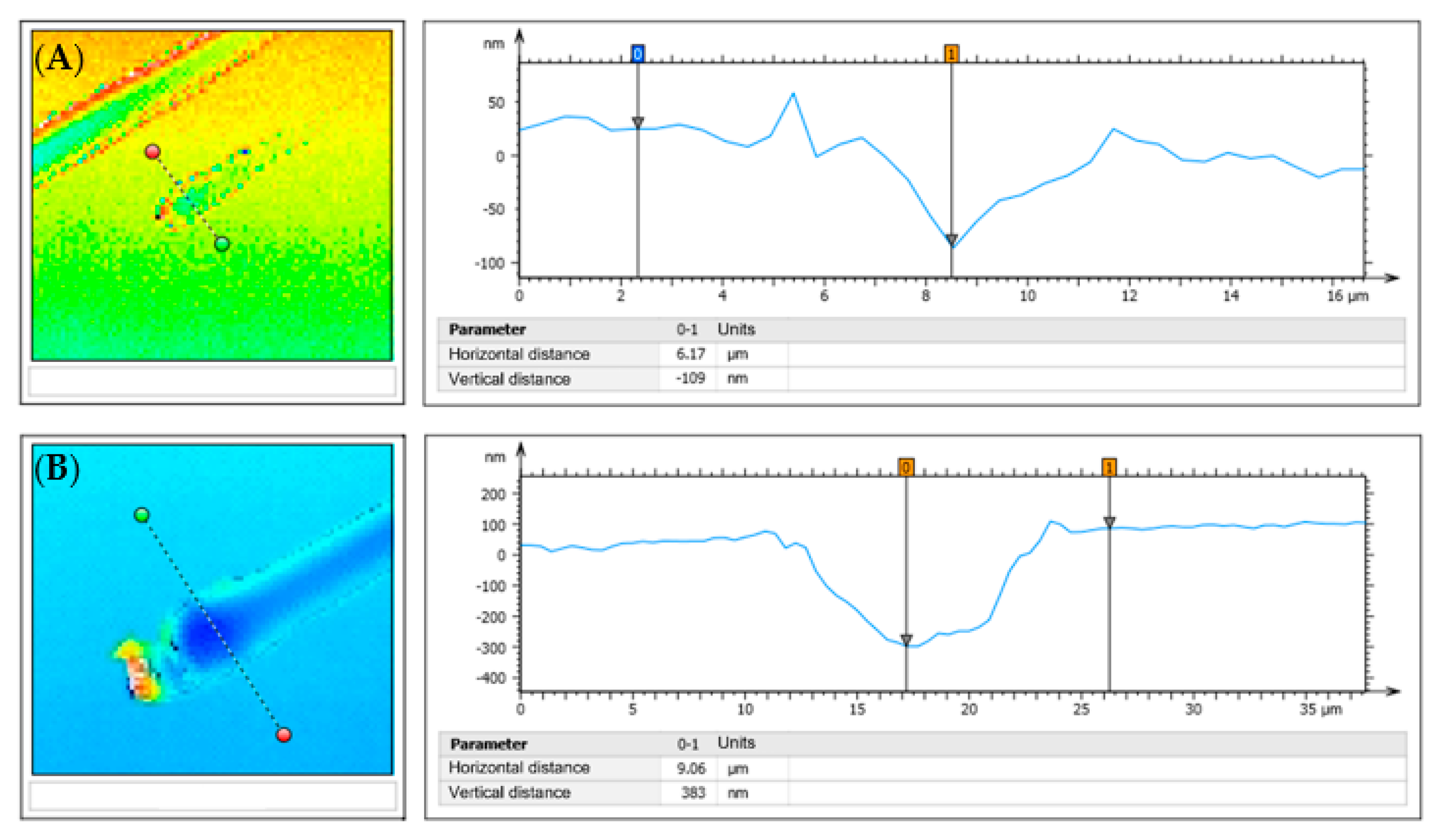
  • Contact position on the contact pads: The heater structures were connected to the measurement setup using contact needles. The contact positions were chosen in such a way that the distance to the heater itself was as large or as small as possible. A depiction thereof is shown in Figure 7.
  • Contact force: It is possible to apply different contact forces to the needles. Unfortunately, there was no way to measure exact forces in this setup. Consequently, undefined small and high contact forces were specified through the penetration depth into the gold contact pad. This penetration depth was obtained using the LSM. The measurement results are illustrated in Figure 8. Contact force 1 corresponded to a penetration depth of 100 nm, and contact force 2 corresponded to a penetration depth of 380 nm.
  • Measurement delay: This parameter defined how long the LIA stayed at one frequency to ensure a stable signal before executing the measurement. This was important because after approaching a new measurement frequency, the sample needs some time to adjust, as the thermal wave is dependent on the frequency and therefore changes after each frequency step. Two measurements were carried out; the delay time was set to 5 s for the first and to 20 s for the second measurement.
  • Damaged pad structure: It should be obvious that damaged structures influence the measurement. However, already, minor damages, as shown in Figure 7 on the left side of the second contact point, did significantly influence the measurement and therefore could not be ignored.
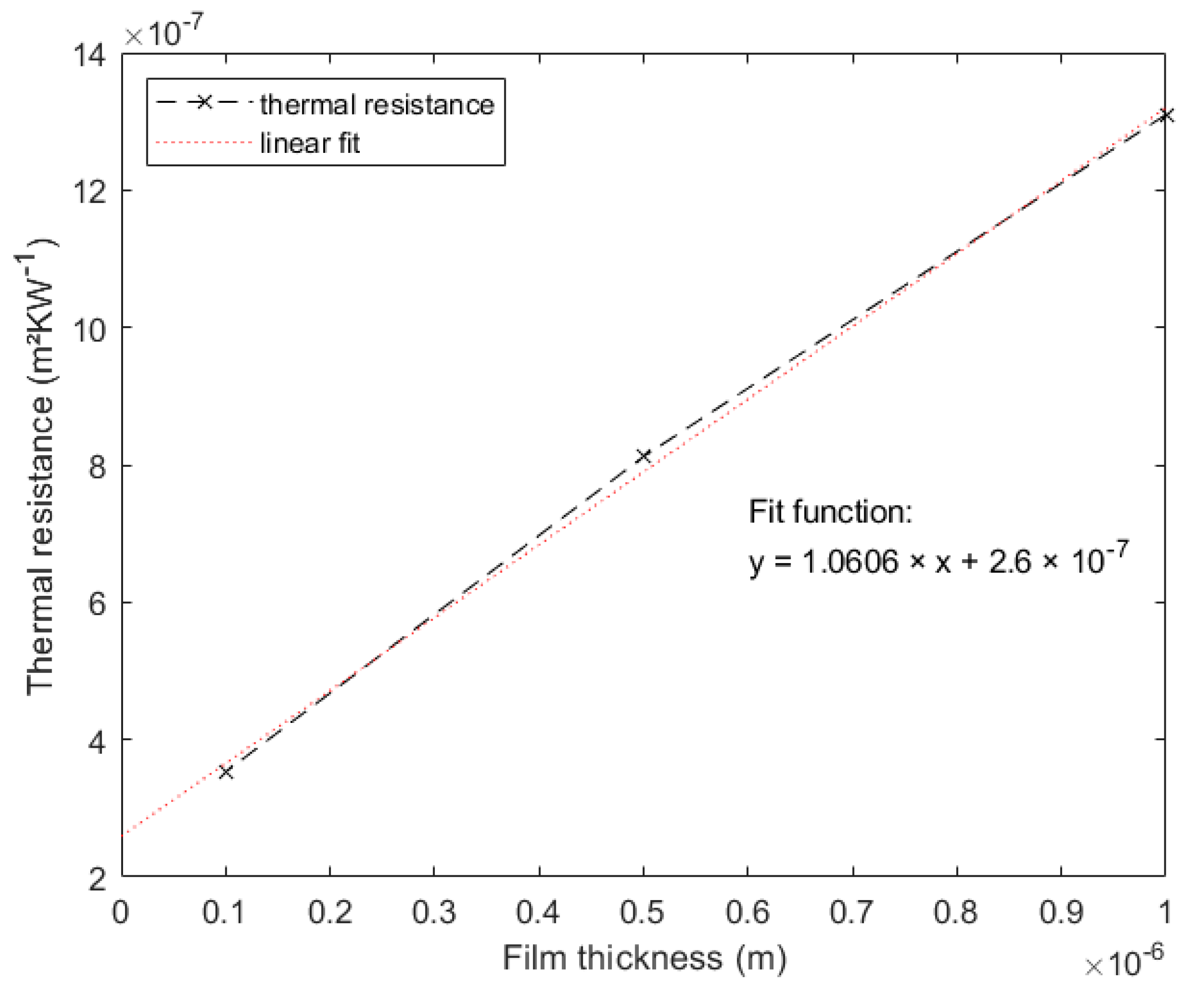
  • Native oxide layer: A native oxide layer forms on top of the substrate before any film can be deposited. To obtain the exact thickness of this layer, a pure substrate wafer was examined using a special ellipsometer, indicating a native oxide thickness of 1.03 nm. This finding was supported by Morita et al. [48]. Even if assuming a very low thermal conductivity of 0.15 Wm−1 K−1 for this oxide layer, the thermal resistance was 6.9 × 10⁻⁹ m2 KW−1, which was around two magnitudes lower than the total interface resistance of the samples (Ri = 2.6 × 10⁻⁷ m2 KW−1) and could therefore be neglected. It should be noted that the ellipsometer measurement result included airborne molecular contamination (AMC). AMC contributes typically to half of the measured thickness and is removed prior to thin film deposition by heating. Thus, the real native oxide thermal resistance was even lower. SiO2 and Al2O3 are both inert against oxidation in air or water, and therefore, no oxide could form on top of the deposited thin film.
  • Influence of heater temperature on thin films: According to FEM simulations carried out in COMSOL Multiphysics® (version 6, 2021, Comsol Multiphysics GmbH, Göttingen, Germany) the maximum DC temperature rise was 1.69 K, and the temperature amplitude was 1.78 K. Thus, the heater temperature rise was much lower than the deposition temperatures of 400 °C and 350 °C for SiO2 and Al2O3, respectively. Therefore, no change in thin film properties was expected.
As depicted in Table 4, the results showed that the heater structure had to be in flawless condition for stable and precise results, while all other parameters did not influence the measurement result significantly.

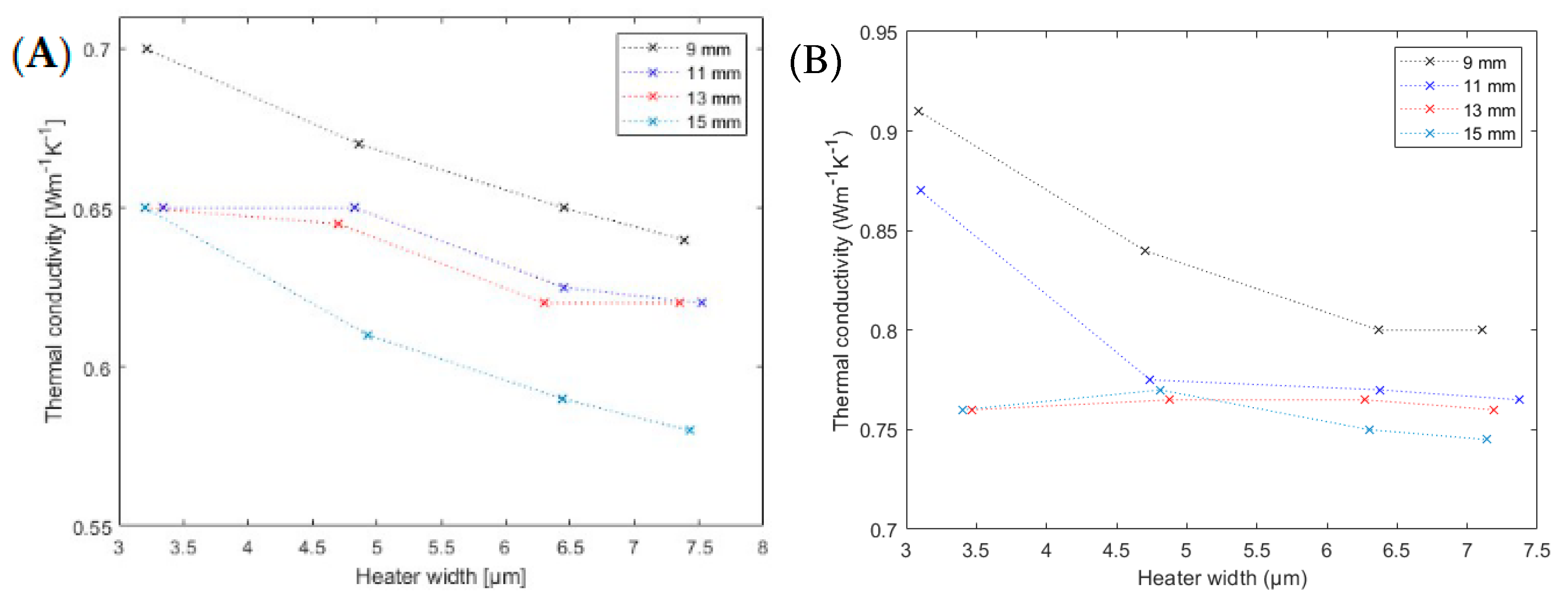
3.3. Silicon Dioxide

The material of interest in this section was SiO2, as for this material, plenty of thermal conductivity data for different film thicknesses are available, as can be seen in Table 2. With this data, the measurement results could be verified, and proper investigation of the heater geometry could be performed. Each measurement was repeated at least two times. Between measurements of the same geometry, at least one hour passed to guarantee that the heater and thin film below had sufficient time to cool down and return to their original states.
First, the sample with a film thickness of 107 nm was investigated. The results can be seen in Figure 9. The approximations suggested that a greater heater width should lead to a more precise result, because the cross-plane thermal conductivity influence becomes dominant. Three of the four heaters, namely the 9 mm-, 11 mm-, and 13 mm-long heaters, showed exactly this behavior. The graphs flattened out for greater heater widths, and it seemed as if they approached a certain value. This stable value was already reached for the 11 mm- and 13 mm-long heaters. Furthermore, these two heaters approached the exact same thermal conductivity value, and therefore, these two lengths seemed to yield the most reliable results. The 9 mm-long heater could approach the same value as the wider heaters, while the 15 mm-long heater drifted away after initially approaching a similar value. The reason for the latter behavior is unknown, and more research has to be done to ascertain it.
To verify these assumptions, the results for the 510 nm and 1018 nm thin films are illustrated in Figure 10. For those two samples, the requirements shown in Table 1 were not truly fulfilled, but the deviation was quite small, and the results should therefore still be reasonable. As both graphs showed similar behavior as stated before, this assumption seemed to be correct. The heaters with lengths 11 mm and 13 mm approached the same value for greater heater widths, while the 9 mm-long heater approached a slightly higher value. For the 510 nm thin film, the 15 mm-long heater also seemed to approach a certain value, but one considerably lower than our other values. The 11 mm- and 13 mm-long heaters delivered nearly the same values and thus supported our thesis from above. For the 1018 nm thin film, the 15 mm-long heater at first approached a similar value as the 11 mm- and 13 mm-long ones. This was the same as for the 107 nm thin film. Based on these measurements, we can state that both the heaters with lengths of 11 mm and 13 mm delivered correct results for a sufficiently wide heater.
Another way to verify these results is to take a look at the thermal resistance Rf vs. the film thickness. Rf is calculated using [20,25]:
R f = d f k f = R i + d f k i ,
where Ri is the total thermal interface resistance and ki is the intrinsic thermal conductivity. For the thermal conductivities of the films kf, the values for the 11 mm long heaters with a width of 6 µm were chosen. As stated by Yamane et al. [25] and Kim et al. [20], these two values should be linearly dependent for films of which the microstructure is independent of film thickness. This proves true for SiO2. If this was true for our results, it would attest the overall coherence of the previously described measurements. For our measurements, this graph is presented in Figure 11. There was clearly a strong linear dependency, which was underlined by a linear fit with R2 of 0.998. Looking at Equation (17), it becomes clear that it is possible to calculate the total thermal interface resistance and the intrinsic thermal conductivity with the help of Figure 11 and the linear fit equation, where ki = 1/slope = 0.94 Wm−1 K−1 is the slope and Ri = 2.6 × 10⁻⁷ m2 KW−1 is the intersection with the Rf axis.
According to the obtained findings, the thermal conductivity could be obtained by the investigation of either the 11 mm- or 13 mm-long heater wider than 6.5 µm. The results are shown in Table 5.

3.4. Aluminum Oxide

The Al2O3 samples with and without annealing at 1000 °C were investigated using the newfound promising heater structures with a length of 11 mm and widths between 5 and 7 µm. The results are shown in Figure 12.
As expected, both samples showed the desired trend and approached a stable value. The final thermal conductivity values can be seen in Table 6. As described in Section 2.4, after the annealing process, the Al2O3 film should no longer have been amorphous, since a certain type of crystallization was observed. Therefore, the thermal conductivity was expected to be higher, which was definitely the case. This thesis has been supported by numerous studies on different materials [49,50,51,52].
There are many different manufacturing processes for Al2O3 films, and therefore, it was quite hard to find good reference values. However, it was possible to find one reference for the sample without annealing that utilized exactly the same procedure as in the present work. Our result correlated with that from reference [53] very well, and therefore, the choice of the heater geometry was confirmed once more. To the best knowledge of the authors, there are no references for the annealed sample yet, as usually, the annealing times in the literature have been in the range of seconds or minutes, while we used an annealing time of 1 h.

4. Conclusions

A detailed inspection of the influence of various heater designs on the cross-plane thermal conductivity of different SiO2 and Al2O3 thin films was conducted. It was demonstrated within over 200 measurements that, even following all commonly used assumptions, the estimated thermal conductivity differs for various heater structures. It was revealed that heater structures of lengths between 11 and 13 mm with widths of 6.5 µm or more delivered reliable results for thin films with thermal conductivities kf < 1 Wm−1 K−1. To further evaluate the quality of the heater designs, tests on Al2O3 thin films were performed so that more reliable results could be obtained. It was demonstrated that the shown annealing process on Al2O3 thin films resulted in a reduction in film thickness and increased thermal conductivity. Furthermore, clear signs of crystallization of the Al2O3 films upon annealing were observed by SEM in the form of cone-shaped grains with diameters of up to 100 nm.

Author Contributions

Conceptualization, F.K.; methodology, F.K.; validation, F.K., C.M., J.W., J.S., G.S.D. and G.B.; formal analysis, F.K.; investigation, F.K.; resources, J.S. and G.B.; data curation, F.K.; writing—original draft preparation, F.K.; writing—review and editing, F.K., C.M., J.W., J.S., G.S.D. and G.B.; visualization, F.K.; supervision, G.S.D. and G.B.; project administration, G.B.; funding acquisition, G.B. All authors have read and agreed to the published version of the manuscript.

Funding

This research was funded by “Bayerisches Staatsministerium für Wirtschaft, Landesentwicklung und Energie StMWi”, grant number DIE-2003-0004//DIE0111/02. The LSM was cofunded by “Deutsche Forschungsgemeinschaft DFG”, grant number INST 926/32-1 FUGG. The APC was funded by Technische Hochschule Deggendorf.

Institutional Review Board Statement

Not applicable.

Informed Consent Statement

Not applicable.

Data Availability Statement

The data presented in this study are available on request from the corresponding author.

Conflicts of Interest

The authors declare no conflict of interest. The sponsors had no role in the design, execution, interpretation, or writing of the study.

References

  1. Nolas, G.S.; Goldsmid, H.J. Thermal Conductivity of semiconductors. In Thermal Conductivity; Springer: Berlin/Heidelberg, Germany, 2004. [Google Scholar] [CrossRef]
  2. Delan, A.; Rennau, M.; Schulz, S.; Gessner, T. Thermal conductivity of ultra low-k dielectrics. Microelectron. Eng. 2003, 70, 280–284. [Google Scholar] [CrossRef]
  3. Zhao, D.; Qian, X.; Gu, X.; Jajja, S.A.; Yang, R. Measurement Techniques for Thermal Conductivity and Interfacial Thermal Conductance of Bulk and Thin Film Materials. J. Electron. Packag. 2016, 138, 040802. [Google Scholar] [CrossRef] [Green Version]
  4. Chien, H.-C.; Yao, D.-J.; Huang, M.-J.; Chang, T.-Y. Thermal conductivity measurement and interface thermal resistance estimation using SiO2 thin film. Rev. Sci. Instrum. 2008, 79, 54902. [Google Scholar] [CrossRef]
  5. Maize, K.; Ezzahri, Y.; Singer, S.; Majumdar, A.; Shakouri, A. Measurement of Thin Film Isotropic and Anisotropic Thermal Conductivity Using 3 Omega and Thermoreflectance Imaging. In Proceedings of the 2008 Twenty-fourth Annual IEEE Semiconductor Thermal Measurement and Management Symposium, San Jose, CA, USA, 16–20 March 2008; IEEE Service Center: Piscataway, NJ, USA, 2008. ISBN 9781424421244. [Google Scholar]
  6. Mayer, P.M.; Lüerssen, D.; Ram, R.J.; Hudgings, J.A. Theoretical and experimental investigation of the thermal resolution and dynamic range of CCD-based thermoreflectance imaging. JOSA A 2007, 24, 1156–1163. [Google Scholar] [CrossRef] [PubMed]
  7. Jiang, P.; Qian, X.; Yang, R. Tutorial: Time-domain thermoreflectance (TDTR) for thermal property characterization of bulk and thin film materials. J. Appl. Phys. 2018, 124, 161103. [Google Scholar] [CrossRef] [Green Version]
  8. Koh, Y.K.; Singer, S.L.; Kim, W.; Zide, J.M.O.; Lu, H.; Cahill, D.G.; Majumdar, A.; Gossard, A.C. Comparison of the 3ω method and time-domain thermoreflectance for measurements of the cross-plane thermal conductivity of epitaxial semiconductors. J. Appl. Phys. 2009, 105, 54303. [Google Scholar] [CrossRef]
  9. Gembarovic, J.; Wang, H.; Apostolescu, S.; Paganelli, D.; Scotto, P. In-plane thermal diffusivity measurement of highly thermal conductive thin films by the flash method. In Proceedings of the 2018 34th Thermal Measurement, Modeling & Management Symposium (SEMI-THERM), San Jose, CA, USA, 19–23 March 2018; IEEE: Piscataway, NJ, USA, 2018; pp. 197–199, ISBN 978-1-5386-4402-7. [Google Scholar]
  10. Baba, T.; Ono, A. Improvement of the laser flash method to reduce uncertainty in thermal diffusivity measurements. Meas. Sci. Technol. 2001, 12, 2046–2057. [Google Scholar] [CrossRef]
  11. Huang, S.; Ruan, X.; Zou, J.; Fu, X.; Yang, H. Thermal conductivity measurement of submicrometer-scale silicon dioxide films by an extended micro-Raman method. Microsyst. Technol. 2009, 15, 837–842. [Google Scholar] [CrossRef]
  12. Soini, M.; Zardo, I.; Uccelli, E.; Funk, S.; Koblmüller, G.; Fontcuberta i Morral, A.; Abstreiter, G. Thermal conductivity of GaAs nanowires studied by micro-Raman spectroscopy combined with laser heating. Appl. Phys. Lett. 2010, 97, 263107. [Google Scholar] [CrossRef]
  13. Metzke, C.; Kühnel, F.; Weber, J.; Benstetter, G. Scanning Thermal Microscopy of Ultrathin Films: Numerical Studies Regarding Cantilever Displacement, Thermal Contact Areas, Heat Fluxes, and Heat Distribution. Nanomaterials 2021, 11, 491. [Google Scholar] [CrossRef]
  14. Metzke, C.; Frammelsberger, W.; Weber, J.; Kühnel, F.; Zhu, K.; Lanza, M.; Benstetter, A.G. On the Limits of Scanning Thermal Microscopy of Ultrathin Films. Materials 2020, 13, 518. [Google Scholar] [CrossRef] [PubMed] [Green Version]
  15. Corbino, O. Thermal ocillations in lamps of thin fibres with alternating current flowing through them and the resulting effect on the rectifier as a result of the presence of even-numbered harmonics. Phys. Z. 1910, 413–417. [Google Scholar]
  16. Corbino, O. Periodic resistance changes of fine metal threads which are brought together by alternating streams as well as deduction of their thermo characteristics at high temperatures. Phys. Z. 1911, 292–295. [Google Scholar]
  17. Birge, N.O.; Nagel, S.R. Wide-frequency specific heat spectrometer. Rev. Sci. Instrum. 1987, 58, 1464–1470. [Google Scholar] [CrossRef]
  18. Cahill, D.G.; Fischer, H.E.; Klitsner, T.; Swartz, E.T.; Pohl, R.O. Thermal conductivity of thin films: Measurements and understanding. J. Vac. Sci. Technol. A Vac. Surf. Films 1989, 7, 1259–1266. [Google Scholar] [CrossRef]
  19. Lee, S.-M.; Cahill, D.G. Heat transport in thin dielectric films. J. Appl. Phys. 1997, 81, 2590–2595. [Google Scholar] [CrossRef]
  20. Kim, J.H.; Feldman, A.; Novotny, D. Application of the three omega thermal conductivity measurement method to a film on a substrate of finite thickness. J. Appl. Phys. 1999, 86, 3959–3963. [Google Scholar] [CrossRef]
  21. Jin, J.; Manoharan, M.P.; Wang, Q.; Haque, M.A. In-plane thermal conductivity of nanoscale polyaniline thin films. Appl. Phys. Lett. 2009, 95, 33113. [Google Scholar] [CrossRef]
  22. Hu, X.J.; Padilla, A.A.; Xu, J.; Fisher, T.S.; Goodson, K.E. 3-Omega Measurements of Vertically Oriented Carbon Nanotubes on Silicon. J. Heat Transf. 2006, 2006, 1109–1113. [Google Scholar] [CrossRef] [Green Version]
  23. Schiffres, S.N.; Malen, J.A. Improved 3-omega measurement of thermal conductivity in liquid, gases, and powders using a metal-coated optical fiber. Rev. Sci. Instrum. 2011, 82, 64903. [Google Scholar] [CrossRef] [Green Version]
  24. Jain, A.; Goodson, K.E. Measurement of the thermal conductivity and heat capacity of freestanding shape memory thin films using the 3 omega method. J. Heat Transf. 2008, 2008, 102402. [Google Scholar] [CrossRef] [Green Version]
  25. Yamane, T.; Nagai, N.; Katayama, S.; Todoki, M. Measurement of thermal conductivity of silicon dioxide thin films using a 3ω method. J. Appl. Phys. 2002, 91, 9772. [Google Scholar] [CrossRef]
  26. Shenoy, S.; Barrera, E.V.; Bayazitoglu, Y. Non-Fourier 3-Omega Method for Thermal Conductivity Measurement. Nanoscale Microscale Thermophys. Eng. 2010, 14, 123–136. [Google Scholar] [CrossRef]
  27. Borca-Tasciuc, T.; Kumar, A.R.; Chen, G. Data Reduction in 3 Omega Method for THin-Film Thermal Conductivity Determination. Rev. Sci. Instrum. 2001, 2001, 2139–2147. [Google Scholar] [CrossRef]
  28. Cahill, D.G. Thermal conductivity measurement from 30 to 750 K: The 3ω method. Rev. Sci. Instrum. 1990, 61, 802–808. [Google Scholar] [CrossRef]
  29. Ramu, A.T.; Bowers, J.E. Analysis of the “3-Omega” method for substrates and thick films of anisotropic thermal conductivity. J. Appl. Phys. 2012, 112, 43516. [Google Scholar] [CrossRef] [Green Version]
  30. Chen, G.; Zhou, S.G.; Yao, D.-Y.; Kim, C.J.; Zheng, X.Y.; Liu, Z.L.; Wang, K.L. Heat Conduction in Alloy-Based Superlattices. In Proceedings of the 17th International Conference on Thermoelectrics, Nagoya, Japan, 28 May 1998; pp. 202–205. [Google Scholar]
  31. Katz, J.S.; Barako, M.T.; Park, W.; Sood, A.; Asheghi, M.; Goodson, K.E. Highly Anisotropic Thermal Conductivity in Spin-Cast Polystyrene Nano-Films. In Proceedings of the 2018 17th IEEE Intersociety Conference on Thermal and Thermomechanical Phenomena in Electronic Systems (ITherm), San Diego, CA, USA, 29 May–1 June 2018; IEEE: Piscataway, NJ, USA, 2018; pp. 477–481, ISBN 978-1-5386-1272-9. [Google Scholar]
  32. Dames, C. Measuring the Thermal Conductivity of Thin Films: 3 Omega and Related Electrothermal Methods. Annu. Rev. Heat Transf. 2013, 16, 7–49. [Google Scholar] [CrossRef]
  33. Tanaka, S.; Takiishi, M.; Miyazaki, K.; Tsukamoto, H. Measurements of Thermal Conductivity of Thin Films by 3-omega Method. In Proceedings of the Micro/Nanoscale Heat Transfer International Conference, Tainan, Taiwan, 6–9 June 2008. [Google Scholar]
  34. Raudzis, C.E. Anwendung und Erweiterung der 3 Omega Methode zur Charakterisierung Komplexer Mehrschichtsysteme in der Mikrosystemtechnik. Ph.D. Thesis, Eberhard-Karls-Universität zu Tübingen, Tübingen, Germany, 2007. [Google Scholar]
  35. Raudzis, C.E.; Schatz, F.; Wharam, D. Extending the 3ω method for thin-film analysis to high frequencies. J. Appl. Phys. 2003, 93, 6050–6055. [Google Scholar] [CrossRef]
  36. Feldman, A. Algorithm for solutions of the thermal diffusion equation in a stratified medium with a modulated heating source. High Temp.-High Press. 1999, 31, 293–298. [Google Scholar] [CrossRef] [Green Version]
  37. Ju, Y.S.; Goodson, K.E. process-dependent thermal transport properties of silicon-dioxide films deposited using low-pressure chemical vapor deposition. J. Appl. Phys. 1999, 1999, 7130–7134. [Google Scholar] [CrossRef] [Green Version]
  38. Jaber, W.; Chapuis, P.-O. Non-idealities in the 3 ω method for thermal characterization in the low- and high-frequency regimes. AIP Adv. 2018, 8, 45111. [Google Scholar] [CrossRef] [Green Version]
  39. Zhang, L.; Jiang, H.C.; Liu, C.; Dong, J.W.; Chow, P. Annealing of Al2O3 thin films prepared by atomic layer deposition. J. Phys. D Appl. Phys. 2007, 40, 3707–3713. [Google Scholar] [CrossRef]
  40. Huff, H.R.; Gilmer, D.C. High Dielectric Constant Materials: VLSI MOSFET Applications; Springer: Berlin/Heidelberg, Germany, 2005; ISBN 3540210814. [Google Scholar]
  41. Griffin, A.J.; Brotzen, F.R.; Loos, P.J. Effect of thickness on the transverse thermal conductivity of thin dielectric films. J. Appl. Phys. 1994, 75, 3761–3764. [Google Scholar] [CrossRef]
  42. Goodson, K.E.; Flik, M.I.; Su, L.T.; Antoniadis, D.A. Annealing-temperature dependence of the thermal conductivity of LPCVD silicon-dioxide layers. IEEE Electron Device Lett. 1993, 14, 490–492. [Google Scholar] [CrossRef]
  43. Govorkov, S.; Ruderman, W.; Horn, M.W.; Goodman, R.B.; Rothschild, M. A new method for measuring thermal conductivity of thin films. Rev. Sci. Instrum. 1997, 68, 3828–3834. [Google Scholar] [CrossRef]
  44. Cahill, D.G.; Allen, T.H. Thermal conductivity of sputtered and evaporated SiO2 and TiO2 optical coatings. Appl. Phys. Lett. 1994, 65, 309–311. [Google Scholar] [CrossRef]
  45. Aarik, J.; Kasikov, A.; Kirm, M.; Lange, S.; Uustare, T.; Mändar, H. Optical properties of crystalline Al2O3 thin films grown by atomic layer deposition. In Proceedings of the Society of Photo-Optical Instrumentation Engineers (SPIE): 4th International Conference on Advanced Optical Materials and Devices, Tartu, Estonia, 6–9 July 2004; pp. 1–10. [Google Scholar]
  46. Wang, Z.-Y.; Zhang, R.-J.; Lu, H.-L.; Chen, X.; Sun, Y.; Zhang, Y.; Wei, Y.-F.; Xu, J.-P.; Wang, S.-Y.; Zheng, Y.-X.; et al. The impact of thickness and thermal annealing on refractive index for aluminum oxide thin films deposited by atomic layer deposition. Nanoscale Res. Lett. 2015, 10, 46. [Google Scholar] [CrossRef] [Green Version]
  47. Jakschik, S.; Schroeder, U.; Hecht, T.; Gutsche, M.; Seidl, H.; Bartha, J.W. Crystallization behavior of thin ALD-Al2O3 films. Thin Solid Films 2002, 425, 216–220. [Google Scholar] [CrossRef]
  48. Morita, M.; Ohmi, T.; Hasegawa, E.; Kawakami, M.; Ohwada, M. Growth of native oxide on a silicon surface. J. Appl. Phys. 1990, 68, 1272–1281. [Google Scholar] [CrossRef]
  49. Foley, B.M.; Brown-Shaklee, H.J.; Duda, J.C.; Cheaito, R.; Gibbons, B.J.; Medlin, D.; Ihlefeld, J.F.; Hopkins, P.E. Thermal conductivity of nano-grained SrTiO3 thin films. Appl. Phys. Lett. 2012, 101, 231908. [Google Scholar] [CrossRef] [Green Version]
  50. Lee, Y.-J.; Park, Y.-H.; Hinoki, T. Influence of Grain Size on Thermal Conductivity of SiC Ceramics. IOP Conf. Ser. Mater. Sci. Eng. 2011, 18, 162014. [Google Scholar] [CrossRef]
  51. Liu, W.L.; Shamsa, M.; Calizo, I.; Balandin, A.A.; Ralchenko, V.; Popovich, A.; Saveliev, A. Thermal conduction in nanocrystalline diamond films: Effects of the grain boundary scattering and nitrogen doping. Appl. Phys. Lett. 2006, 89, 171915. [Google Scholar] [CrossRef] [Green Version]
  52. Mishra, V.; Garay, J.E.; Dames, C. Leveraging Anisotropy for Coupled Optimization of Thermal Transport and Light Transmission in Micro-Structured Materials for High-Power Laser Applications. Adv. Theory Simul. 2020, 3, 2000036. [Google Scholar] [CrossRef]
  53. Makris, A.; Haeger, T.; Heiderhoff, R.; Riedl, T. From diffusive to ballistic Stefan–Boltzmann heat transport in thin non-crystalline films. RSC Adv. 2016, 6, 94193–94199. [Google Scholar] [CrossRef] [Green Version]
Figure 1. (A) Wheatstone bridge layout. R1 and R2 are high-precision resistances chosen in such a way that most of the current passes through the heater, Rv is a variable decade resistance, and Rs is the sample resistance. (B) 3ω metal heater deposited on top of a SiO2 thin film with length l, width 2b, and two contact pads on each side. Heaters in this work had theoretical lengths from 9 to 15 mm and widths from 2 to 6 µm. The image is not depicted to scale.
Nanomaterials 12 01928 g001
Figure 2. Z-scan performed with LSM: (A) 3D image created from z-scan showing the contact pads and the heater line itself. (B) Cross-section of the heater along the marker in (A).
Nanomaterials 12 01928 g002
Figure 3. Scanning electron microscope (SEM) image of a cross-section of Al2O3 thin film samples (A) without annealing and (B) with annealing at 1000 °C.
Nanomaterials 12 01928 g003
Figure 4. Cross-sectional SEM images of a heater structure (produced with FIB-cut). The Pt layer on top of the heater was used to protect the surface from damage due to the FIB process. It was deposited only on this specific sample and was not present on the devices that were measured. (A) shows a cross-section of a sample with substrate, thin film, and heater from bottom to top. (B) shows a cross-section of the heater, revealing the titanium (70.8 nm), platinum (55.1 nm), and gold (483.2 nm) stack.
Nanomaterials 12 01928 g004
Figure 5. (A) Optical image of a complete wafer with repeating 3ω structures. (B) Optical microscope image of a full set of 16 heaters with different lengths and widths (zoomed into (A)). (C) Microscopic image of the contact pads on each side (zoomed into (B)).
Nanomaterials 12 01928 g005
Figure 6. TCR measurement of 11 mm-long gold heater with 5 µm width on silicon dioxide thin film. Electrical resistance was measured at temperatures between 30 and 80 °C in steps of 10 °C. The resistance at measurement temperature Rh,0 = 113.7 Ω.
Nanomaterials 12 01928 g006
Figure 7. Contact pad of 3-Omega structure with two different contact positions. The positions were mirrored on the second contact pad. To the left of the second contact point, slight damage was induced to the contact pad after all other measurements were carried out.
Nanomaterials 12 01928 g007
Figure 8. LSM measurements of penetration depths for (A) contact force 1 and (B) contact force 2. The left images show the complete LSM scans, while the right images show the cross-sections indicated in the left images.
Nanomaterials 12 01928 g008
Figure 9. Measured thermal conductivity of 100 nm thin SiO2 film. The different colors correspond to different heater lengths as indicated in the inset.
Nanomaterials 12 01928 g009
Figure 10. Measured thermal conductivity of (A) 500 nm and (B) 1000 nm thin SiO2 films. The different colors correspond to different heater lengths as indicated in the inset.
Nanomaterials 12 01928 g010
Figure 11. Thermal resistance of SiO2 thin film for different film thicknesses. A linear fit with the corresponding fit function is displayed, also.
Nanomaterials 12 01928 g011
Figure 12. Measurement results for the 115 nm thin Al2O3 film and the 102.7 nm thin Al2O3 film with annealing at 1000 °C.
Nanomaterials 12 01928 g012
Table 1. Requirements for choosing valid heater geometries and measurement frequencies.
Desired ApproximationEquation
Film heat flow is quasistatic, indicating that the material does not store energy and heat spreads equally [32,37] λ f d f > 5.7
Substrate is semi-infinite [27,32] d s λ s > 2
Heater counts as a line source [27,32] λ s b > 5
Heater counts as infinitely long [32] l λ s > 2
Heater is considered massless to neglect the volumetric heat capacity of the heater [27,32,37] ( c h × p h c f × p f ) ( d h × d f λ f 2 ) < 0.01
Convection and radiation losses are negligible [28,32] m a x [ ( h × d f k f ) , ( h × λ s 2 k s ) ] < 0.01
Substrate is isothermal [27,32] ( k f k s ) 2 < 0.01
Heat flow through thin film is one dimensional [27,32] ( b d f ) ( k f z k f x ) 1 2 > 5.5
Heater thickness does not influence measurement [38] d h 2 b < 0.05
Influence of native oxide layer is neglectable [38,39] π × k s × 2 × 10 9 2 b × k f z × l n ( d s b ) + 1.0484 < 0.01
Influence of contact pads is neglectable [38] l 2 b > 600
Heater counts as uniform heat source [32] ( d h × d f b 2 ) ( k h k f ) < 1
Table 2. Literature values of the thermal conductivity of silicon dioxide for different film thicknesses. The last 3 rows sum up all shown references.
Film Thickness
(nm)
Thermal Conductivity
(Wm−1 K−1)
Reference
1000.05–0.08Griffin, 1994 [41]
1000.73–0.9Lee, 1997 [19]
2000.85–1.15Goodson, 1993 [42]
5000.2–0.3Griffin, 1994 [41]
5000.59–0.77Govorkov, 1997 [43]
5001.15–1.4Goodson, 1993 [42]
10000.35–0.6Griffin, 1994 [41]
10000.59–0.61Govorkov, 1997 [43]
10000.1–1.3Cahill, 1994 [44]
1000.05–0.9-
5000.2–1.4-
10000.35–1.3-
Table 3. Overview of all sample materials, deposition methods, film thicknesses, and annealing temperatures.
Bulk MaterialFilm MaterialDeposition MethodFilm Thickness
(nm)
Annealing Temperature
(°C)
SiSiO2PECVD107
SiSiO2PECVD510
SiSiO2PECVD1018
SiAl2O3LP ALD115
SiAl2O3LP ALD102.71000
Table 4. Results for different potential measurement influences for a 1 µm thin SiO2 thin film. The deployed heater geometry, investigated parameters, and measurement results are shown.
Heater Length
(mm)
Heater Width
(µm)
Balancing Frequency
(Hz)
Thermal Conductivity
(Wm−1 K−1)
11.0863.101000.84
11.0863.10500 0.83
11.0863.1010000.83
Contact position
13.0963.4710.72
13.0963.4720.72
Contact force
13.0984.8810.73
13.0984.8820.73
Measurement delay
11.0926.385 s0.77
11.0926.3820 s0.77
Pad condition
13.0963.47intact0.72
13.0963.47damaged0.68
Table 5. Final measurement results for different SiO2 thin films.
Film Thickness
(nm)
Thermal Conductivity
(Wm−1 K−1)
Reference Values
(Wm−1 K−1)
1070.280.05–0.9 [19,41]
5100.620.2–1.4 [41,42,43]
10180.770.35–1.3 [41,43,44]
Table 6. Final thermal conductivity measurement results for the different Al2O3 samples.
Annealing Temperature
(°C)
Film Thickness
(nm)
Thermal Conductivity
(Wm−1 K−1)
Reference Value
(Wm−1 K−1)
-1150.810.8 [53]
1000102.70.93-
Publisher’s Note: MDPI stays neutral with regard to jurisdictional claims in published maps and institutional affiliations.

