
Copper Hexacyanoferrate Thin Film Deposition and Its Application to a New Method for Diffusion Coefficient Measurement

 , and
, and 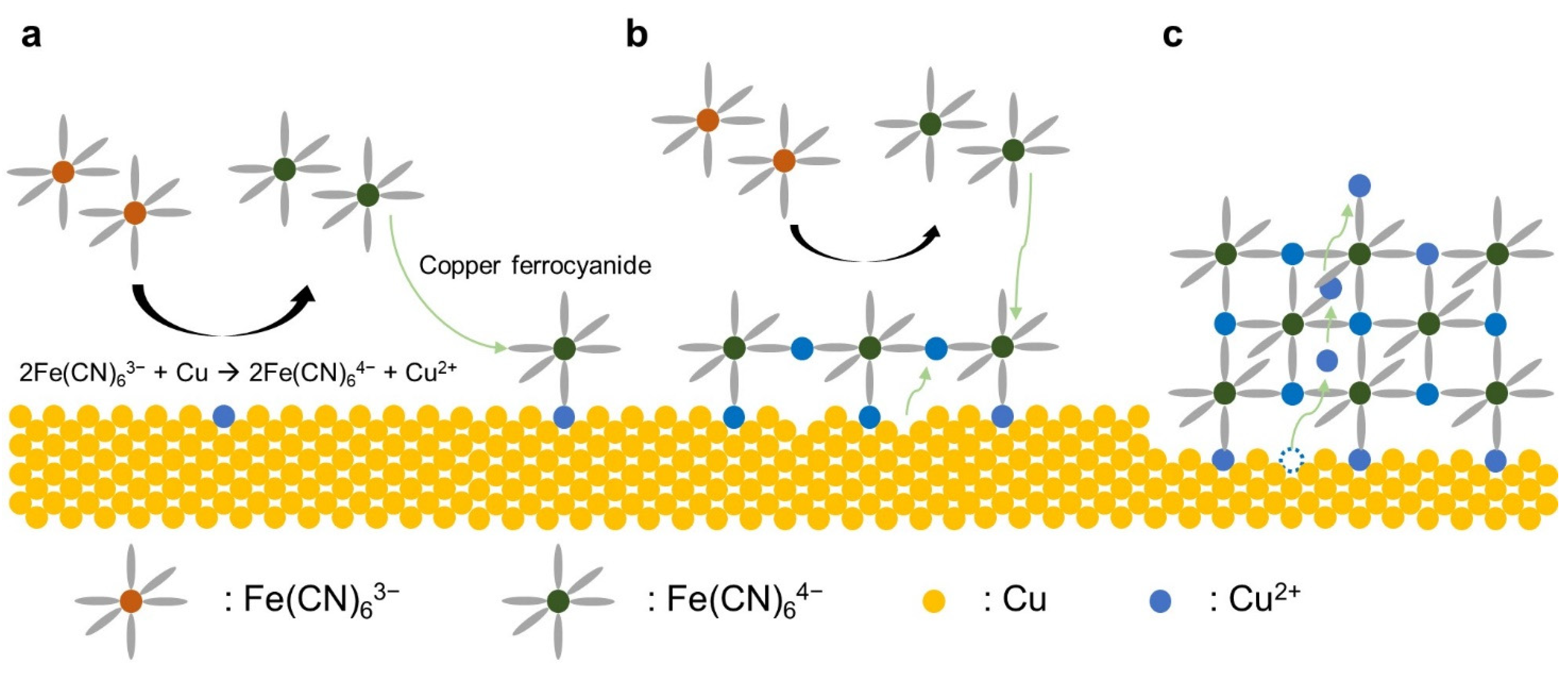
Abstract
:1. Introduction
2. Materials and Methods
2.1. Materials
2.2. Deposition of CuHCFe Thin Film
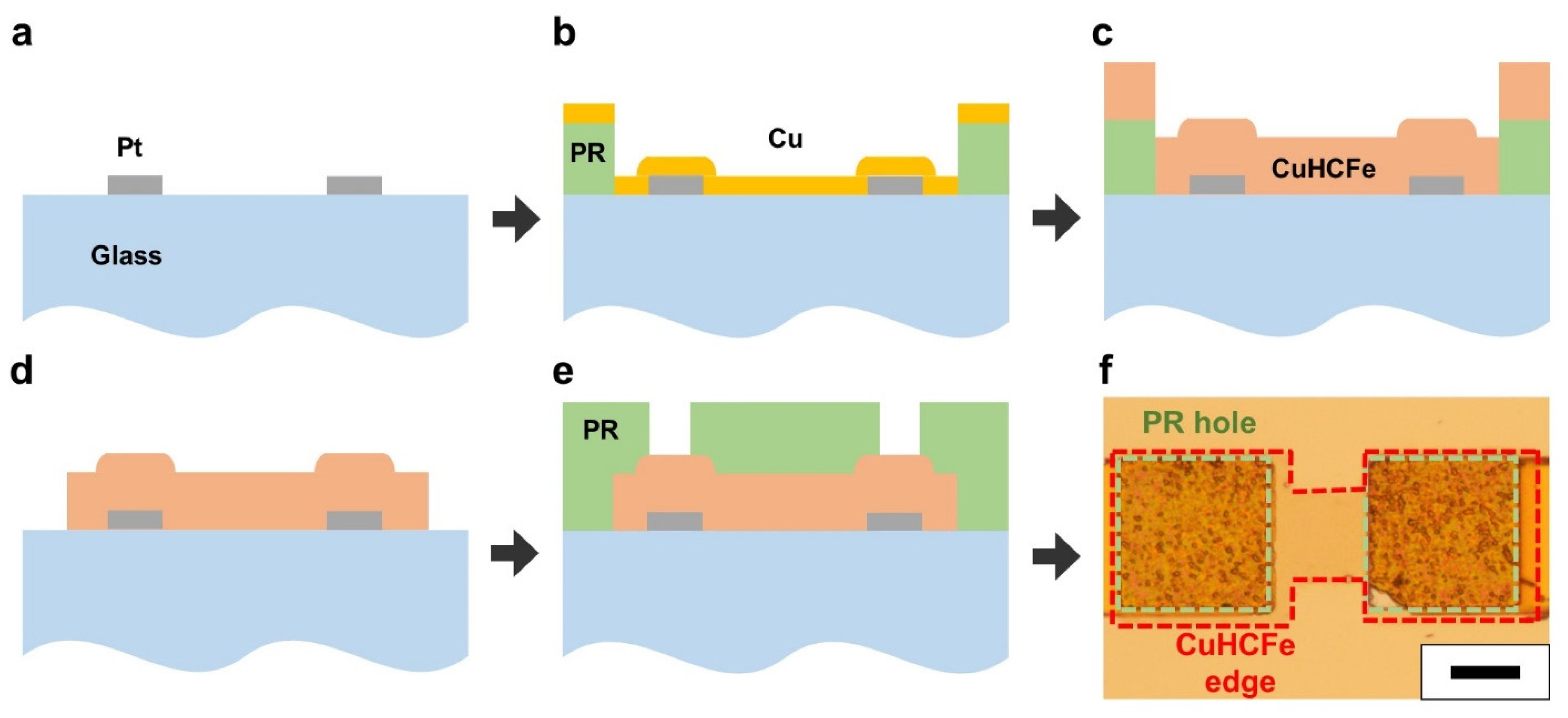
2.3. Micropatterning of CuHCFe Thin Film
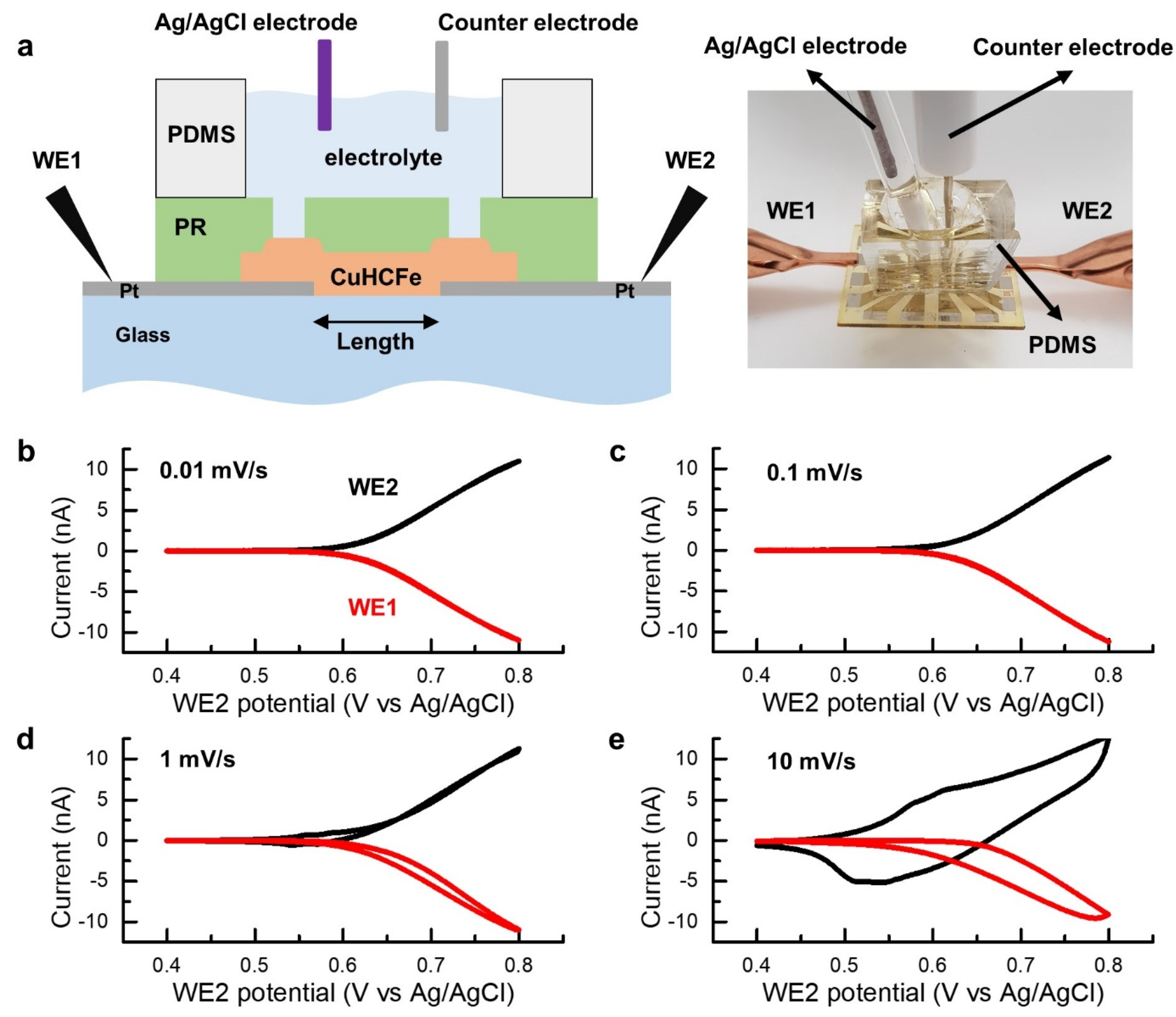
2.4. Electrochemical Characterization of CuHCFe Thin Films
2.5. Characterization of CuHCFe Thin Film
3. Results and Discussion
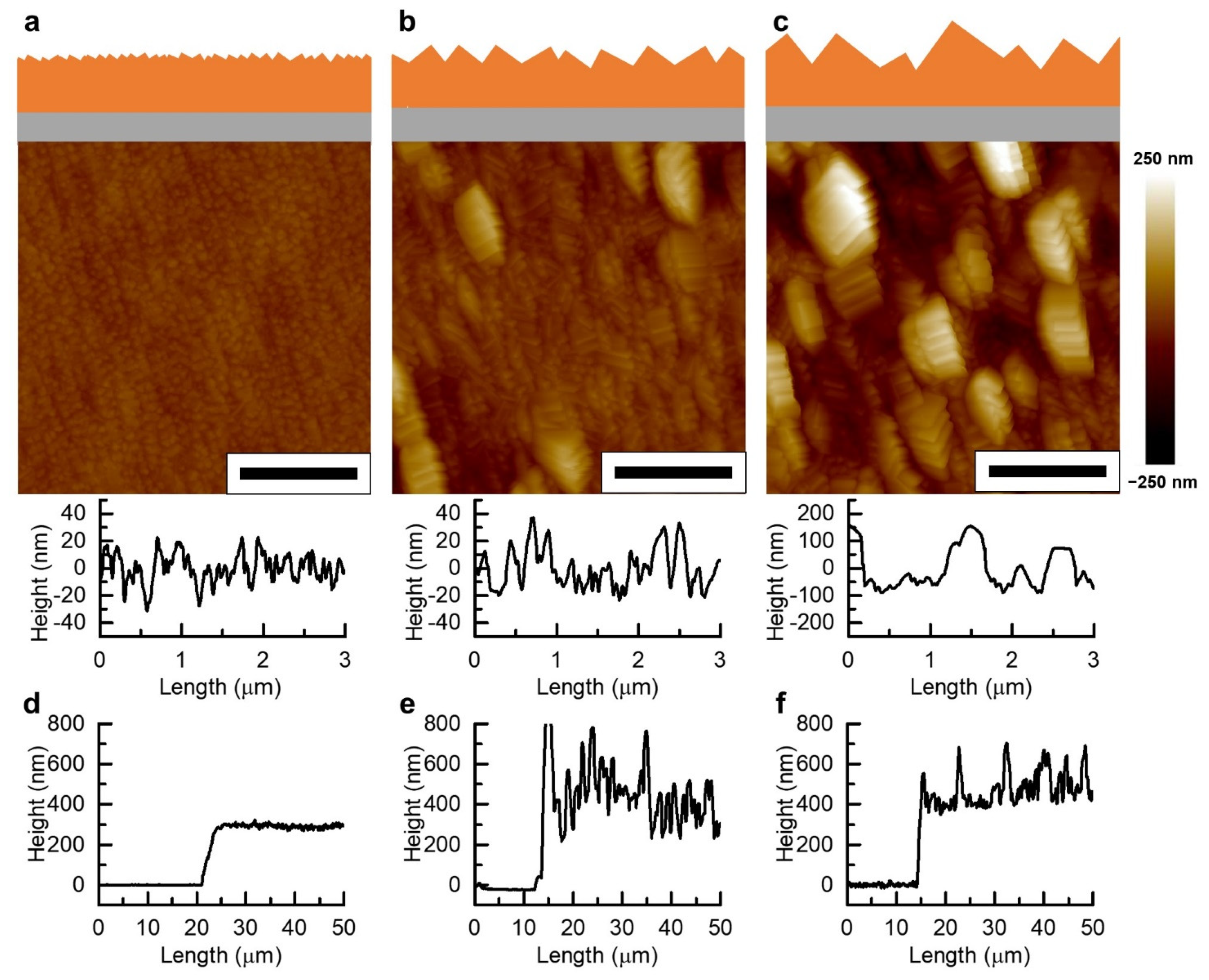
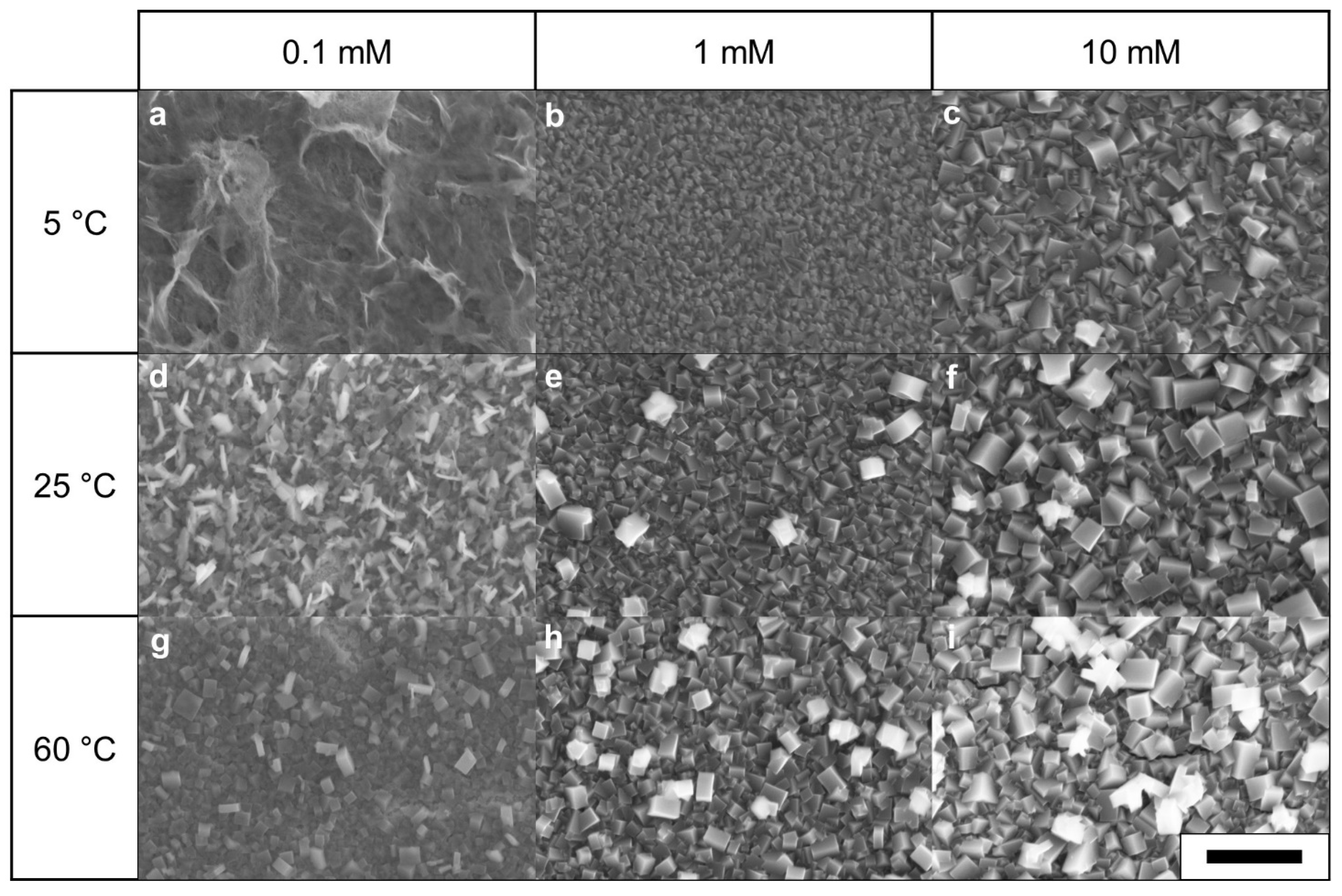
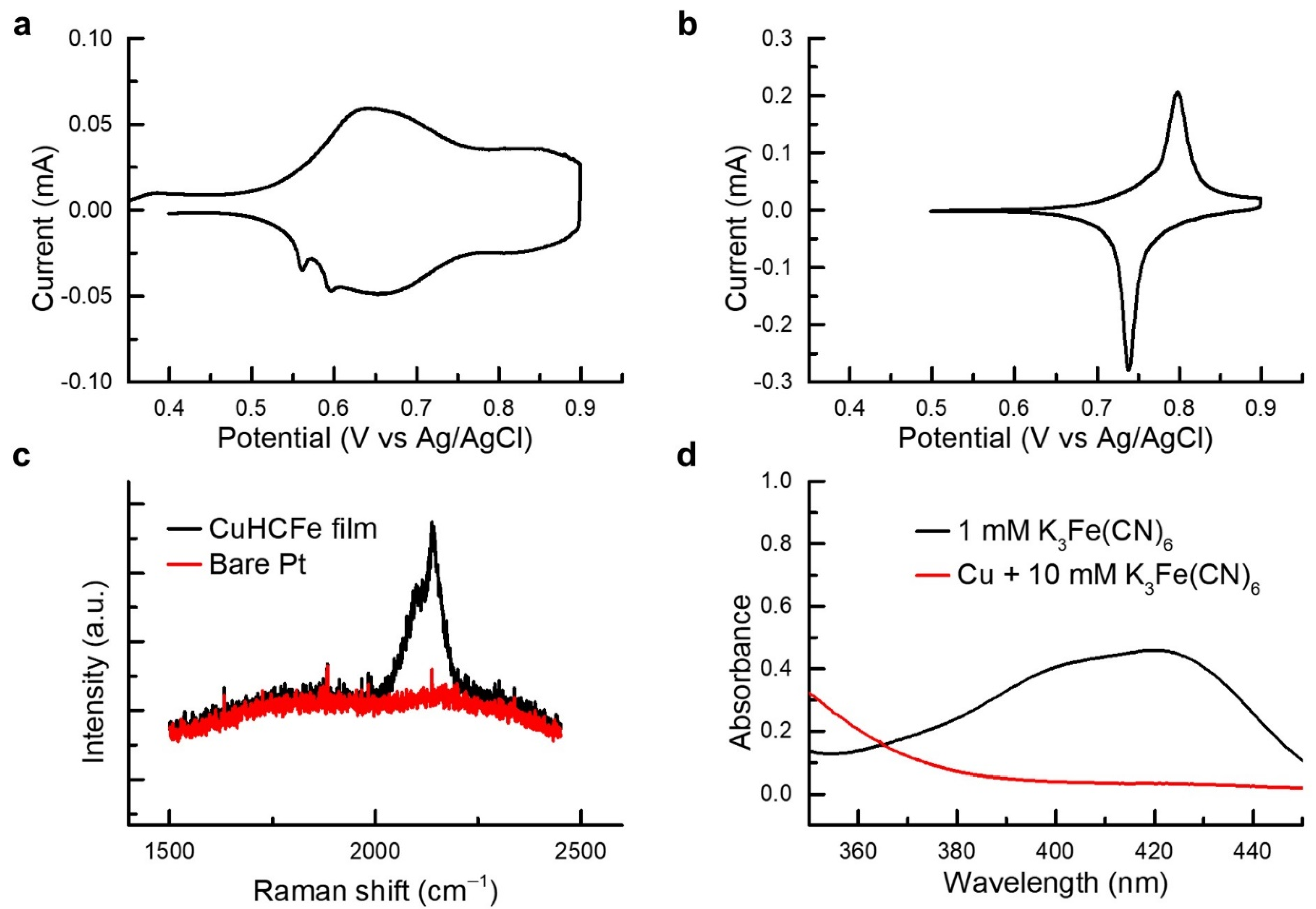
3.1. CuHCFe Thin Film Deposition
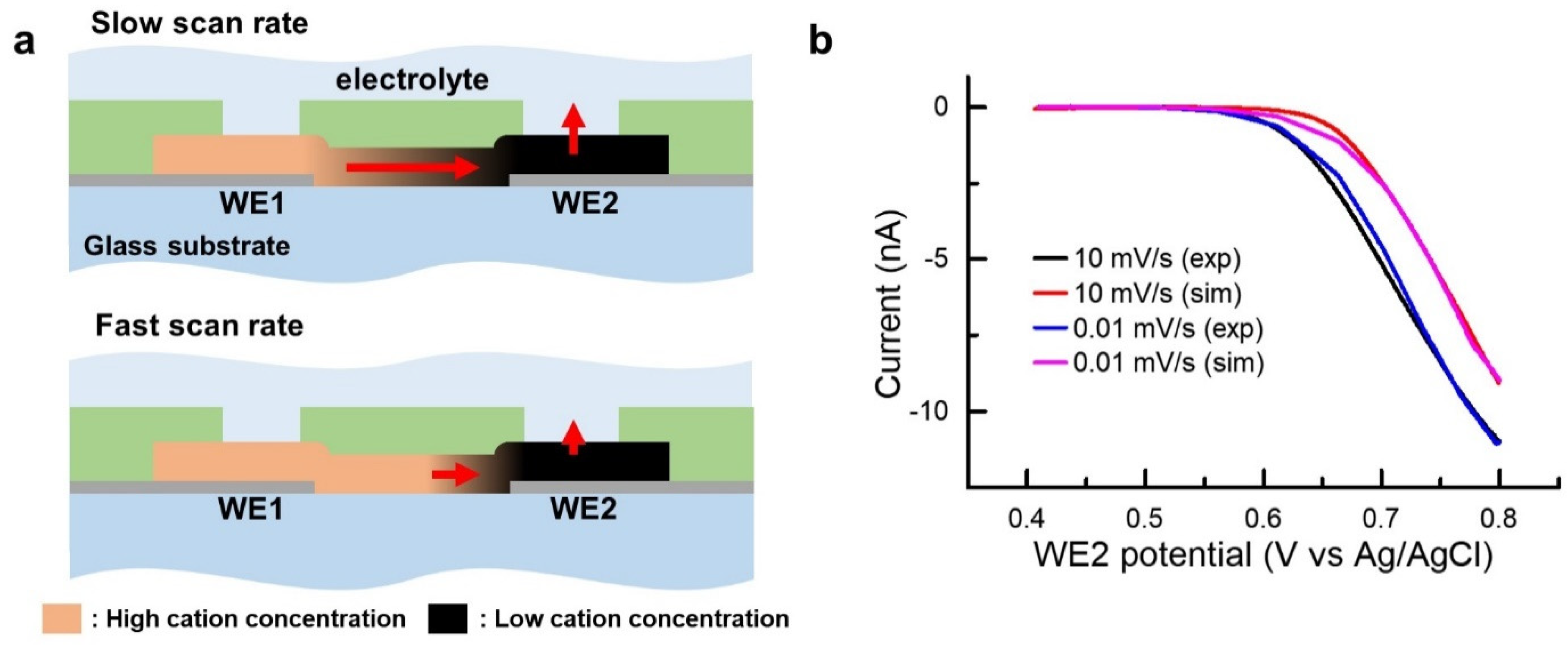
3.2. Micropatterning of CuHCFe Thin Film and Fabrication of Microelectrochemical System of CuHCFe
4. Conclusions
Supplementary Materials
Author Contributions
Funding
Data Availability Statement
Conflicts of Interest
References
- Karyakin, A.A. Prussian Blue and Its Analogues: Electrochemistry and Analytical Applications. Electroanalysis 2001, 13, 813–819. [Google Scholar] [CrossRef]
- Karyakin, A. Advances of Prussian blue and its analogues in (bio)sensors. Curr. Opin. Electrochem. 2017, 5, 92–98. [Google Scholar] [CrossRef]
- Qian, J.; Wu, C.; Cao, Y.; Ma, Z.-F.; Huang, Y.; Ai, X.; Yang, H. Prussian Blue Cathode Materials for Sodium-Ion Batteries and Other Ion Batteries. Adv. Energy Mater. 2018, 8, 1702619. [Google Scholar] [CrossRef]
- Yun, J.; Zeng, Y.; Kim, M.; Gao, C.; Kim, Y.; Lu, L.; Kim, T.T.-H.; Zhao, W.; Bae, T.-H.; Lee, S.W. Tear-Based Aqueous Batteries for Smart Contact Lenses Enabled by Prussian Blue Analogue Nanocomposites. Nano Lett. 2021, 21, 1659–1665. [Google Scholar] [CrossRef]
- Lee, S.W.; Yang, Y.; Lee, H.-W.; Ghasemi, H.; Kraemer, D.; Chen, G.; Cui, Y. An electrochemical system for efficiently harvesting low-grade heat energy. Nat. Commun. 2014, 5, 3942. [Google Scholar] [CrossRef] [Green Version]
- Hurlbutt, K.; Wheeler, S.; Capone, I.; Pasta, M. Prussian blue analogs as battery materials. Joule 2018, 2, 1950–1960. [Google Scholar] [CrossRef] [Green Version]
- Wessells, C.D.; Huggins, R.A.; Cui, Y. Copper hexacyanoferrate battery electrodes with long cycle life and high power. Nat. Commun. 2011, 2, 550. [Google Scholar] [CrossRef] [Green Version]
- Pasta, M.; Wessells, C.D.; Liu, N.; Nelson, J.; McDowell, M.T.; Huggins, R.A.; Toney, M.F.; Cui, Y. Full open-framework batteries for stationary energy storage. Nat. Commun. 2014, 5, 3007. [Google Scholar] [CrossRef]
- Wu, X.; Hong, J.J.; Shin, W.; Ma, L.; Liu, T.; Bi, X.; Yuan, Y.; Qi, Y.; Surta, T.W.; Huang, W.; et al. Diffusion-free Grotthuss topochemistry for high-rate and long-life proton batteries. Nat. Energy 2019, 4, 123–130. [Google Scholar] [CrossRef]
- Wessells, C.D.; Peddada, S.V.; McDowell, M.T.; Huggins, R.A.; Cui, Y. The Effect of Insertion Species on Nanostructured Open Framework Hexacyanoferrate Battery Electrodes. J. Electrochem. Soc. 2011, 159, A98–A103. [Google Scholar] [CrossRef]
- Liu, Y.; Gao, C.; Sim, S.; Kim, M.; Lee, S.W. Lithium Manganese Oxide in an Aqueous Electrochemical System for Low-Grade Thermal Energy Harvesting. Chem. Mater. 2019, 31, 4379–4384. [Google Scholar] [CrossRef]
- Gao, C.; Liu, Y.; Chen, B.; Yun, J.; Feng, E.; Kim, Y.; Kim, M.; Choi, A.; Lee, H.; Lee, S.W. Efficient Low-Grade Heat Harvesting Enabled by Tuning the Hydration Entropy in an Electrochemical System. Adv. Mater. 2021, 33, 2004717. [Google Scholar] [CrossRef] [PubMed]
- Firouzi, A.; Qiao, R.; Motallebi, S.; Valencia, C.W.; Israel, H.S.; Fujimoto, M.; Wray, L.A.; Chuang, Y.-D.; Yang, W.; Wessells, C.D. Monovalent manganese based anodes and co-solvent electrolyte for stable low-cost high-rate sodium-ion batteries. Nat. Commun. 2018, 9, 861. [Google Scholar] [CrossRef] [Green Version]
- Ji, Z.; Han, B.; Liang, H.; Zhou, C.; Gao, Q.; Xia, K.; Wu, J. On the mechanism of the improved operation voltage of rhombohedral nickel hexacyanoferrate as cathodes for sodium-ion batteries. ACS Appl. Mater. Interfaces 2016, 8, 33619–33625. [Google Scholar] [CrossRef] [PubMed]
- Wu, X.; Wu, C.; Wei, C.; Hu, L.; Qian, J.; Cao, Y.; Ai, X.; Wang, J.; Yang, H. Highly crystallized Na2CoFe(CN)6 with suppressed lattice defects as superior cathode material for sodium-ion batteries. ACS Appl. Mater. Interfaces 2016, 8, 5393–5399. [Google Scholar] [CrossRef] [PubMed]
- You, Y.; Wu, X.-L.; Yin, Y.-X.; Guo, Y.-G. High-quality Prussian blue crystals as superior cathode materials for room-temperature sodium-ion batteries. Energy Environ. Sci. 2014, 7, 1643–1647. [Google Scholar] [CrossRef]
- Li, W.-J.; Chou, S.-L.; Wang, J.-Z.; Kang, Y.-M.; Wang, J.-L.; Liu, Y.; Gu, Q.-F.; Liu, H.-K.; Dou, S.-X. Facile method to synthesize Na-enriched Na1+xFeFe(CN)6 frameworks as cathode with superior electrochemical performance for sodium-ion batteries. Chem. Mater. 2015, 27, 1997–2003. [Google Scholar] [CrossRef] [Green Version]
- Karyakin, A.; Puganova, E.A.; Budashov, I.A.; Kurochkin, I.N.; Karyakina, E.E.; Levchenko, V.A.; Matveyenko, A.V.N.; Varfolomeyev, S.D. Prussian Blue Based Nanoelectrode Arrays for H2O2 Detection. Anal. Chem. 2004, 76, 474–478. [Google Scholar] [CrossRef]
- Mortimer, R.J.; Reynolds, J.R. In situ colorimetric and composite coloration efficiency measurements for electrochromic Prussian blue. J. Mater. Chem. 2005, 15, 2226–2233. [Google Scholar] [CrossRef] [Green Version]
- Kim, M.; Jung, I.D.; Kim, Y.; Yun, J.; Gao, C.; Lee, H.-W.; Lee, S.W. An electrochromic alarm system for smart contact lenses. Sens. Actuators B Chem. 2020, 322, 128601. [Google Scholar] [CrossRef]
- And, N.R.D.T.; Rajeshwar, K.; Lezna, R.O. Metal Hexacyanoferrates: Electrosynthesis, in Situ Characterization, and Applications. Chem. Mater. 2003, 15, 3046–3062. [Google Scholar] [CrossRef]
- Pauliukaite, R.; Florescu, M.; Brett, C.M.A. Characterization of cobalt- and copper hexacyanoferrate-modified carbon film electrodes for redox-mediated biosensors. J. Solid State Electrochem. 2005, 9, 354–362. [Google Scholar] [CrossRef] [Green Version]
- Pyrasch, M.; Tieke, B. Electro- and Photoresponsive Films of Prussian Blue Prepared upon Multiple Sequential Adsorption. Langmuir 2001, 17, 7706–7709. [Google Scholar] [CrossRef]
- Cobo, S.; Molnár, G.; Carcenac, F.; Szilágyi, P.A.; Salmon, L.; Vieu, C.; Bousseksou, A. Thin films of Prussian blue: Sequential assembly, patterning and electron transport properties at the nanometric scale. J. Nanosci. Nanotechnol. 2010, 10, 5042–5050. [Google Scholar] [CrossRef]
- Bellomo, A. Formation of copper (II), zinc (II), silver (I) and lead (II) ferrocyanides. Talanta 1970, 17, 1109–1114. [Google Scholar] [CrossRef]
- Wang, R.; Shyam, B.; Stone, K.; Weker, J.N.; Pasta, M.; Lee, H.-W.; Toney, M.F.; Cui, Y. Reversible Multivalent (Monovalent, Divalent, Trivalent) Ion Insertion in Open Framework Materials. Adv. Energy Mater. 2015, 5, 1401869. [Google Scholar] [CrossRef]
- Buser, H.J.; Schwarzenbach, D.; Petter, W.; Ludi, A. The crystal structure of Prussian Blue: Fe4[Fe(CN)6]3×H2O. Inorg. Chem. 1977, 16, 2704–2710. [Google Scholar] [CrossRef]
- Giorgetti, M.; Guadagnini, L.; Tonelli, D.; Minicucci, M.; Aquilanti, G. Structural characterization of electrodeposited copper hexacyanoferrate films by using a spectroscopic multi-technique approach. Phys. Chem. Chem. Phys. 2012, 14, 5527–5537. [Google Scholar] [CrossRef]
- Chidsey, C.E.D.; Murray, R.W. Redox capacity and direct current electron conductivity in electroactive materials. J. Phys. Chem. 1986, 90, 1479–1484. [Google Scholar] [CrossRef]
- Yang, X.; Rogach, A.L. Electrochemical Techniques in Battery Research: A Tutorial for Nonelectrochemists. Adv. Energy Mater. 2019, 9, 1900747. [Google Scholar] [CrossRef]
- Takachi, M.; Fukuzumi, Y.; Moritomo, Y. Na+ diffusion kinetics in nanoporous metal-hexacyanoferrates. Dalton Trans. 2015, 45, 458–461. [Google Scholar] [CrossRef] [PubMed] [Green Version]
- Wang, W.; Gang, Y.; Hu, Z.; Yan, Z.; Li, W.; Li, Y.; Gu, Q.-F.; Wang, Z.; Chou, S.-L.; Liu, H.-K.; et al. Reversible structural evolution of sodium-rich rhombohedral Prussian blue for sodium-ion batteries. Nat. Commun. 2020, 11, 980. [Google Scholar] [CrossRef] [PubMed] [Green Version]


Publisher’s Note: MDPI stays neutral with regard to jurisdictional claims in published maps and institutional affiliations. |
© 2021 by the authors. Licensee MDPI, Basel, Switzerland. This article is an open access article distributed under the terms and conditions of the Creative Commons Attribution (CC BY) license (https://creativecommons.org/licenses/by/4.0/).
Share and Cite
Yun, J.; Kim, Y.; Gao, C.; Kim, M.; Lee, J.Y.; Lee, C.-H.; Bae, T.-H.; Lee, S.W. Copper Hexacyanoferrate Thin Film Deposition and Its Application to a New Method for Diffusion Coefficient Measurement. Nanomaterials 2021, 11, 1860. https://doi.org/10.3390/nano11071860
Yun J, Kim Y, Gao C, Kim M, Lee JY, Lee C-H, Bae T-H, Lee SW. Copper Hexacyanoferrate Thin Film Deposition and Its Application to a New Method for Diffusion Coefficient Measurement. Nanomaterials. 2021; 11(7):1860. https://doi.org/10.3390/nano11071860
Chicago/Turabian StyleYun, Jeonghun, Yeongae Kim, Caitian Gao, Moobum Kim, Jae Yoon Lee, Chul-Ho Lee, Tae-Hyun Bae, and Seok Woo Lee. 2021. "Copper Hexacyanoferrate Thin Film Deposition and Its Application to a New Method for Diffusion Coefficient Measurement" Nanomaterials 11, no. 7: 1860. https://doi.org/10.3390/nano11071860