Article

Tunable Electronic Properties of Lateral Monolayer Transition Metal Dichalcogenide Superlattice Nanoribbons

by
Jinhua Wang
1,2,* and
Gyaneshwar P. Srivastava
2
1
School of Science, Tianjin University of Technology and Education, Tianjin 300222, China
2
School of Physics, University of Exeter, Exeter EX4 4QL, UK
*
Author to whom correspondence should be addressed.
Nanomaterials 2021, 11(2), 534; https://doi.org/10.3390/nano11020534
Submission received: 5 January 2021 / Revised: 11 February 2021 / Accepted: 12 February 2021 / Published: 19 February 2021

Abstract

:
The structural stability and structural and electronic properties of lateral monolayer transition metal chalcogenide superlattice zigzag and armchair nanoribbons have been studied by employing a first-principles method based on the density functional theory. The main focus is to study the effects of varying the width and periodicity of nanoribbon, varying cationic and anionic elements of superlattice parent compounds, biaxial strain, and nanoribbon edge passivation with different elements. The band gap opens up when the (MoS2)3/(WS2)3 and (MoS2)3/(MoTe2)3 armchair nanoribbons are passivated by H, S and O atoms. The H and O co-passivated (MoS2)3/(WS2)3 armchair nanoribbon exhibits higher energy band gap. The band gap with the edge S vacancy connecting to the W atom is much smaller than the S vacancy connecting to the Mo atom. Small band gaps are obtained for both edge and inside Mo vacancies. There is a clear difference in the band gap states between inside and edge Mo vacancies for symmetric nanoribbon structure, while there is only a slight difference for asymmetric structure. The electronic orbitals of atoms around Mo vacancy play an important role in determining the valence band maximum, conduction band minimum, and impurity level in the band gap.

1. Introduction

Properties of two-dimensional (2D) materials have been the focus of a great deal of experimental and theoretical research over the past few decades due to their unique electronic structure. 2D materials such as graphene, silicene, boron nitride, phosphorene, transition metal chalcogenides (MoS2, WS2, MoTe2, WTe2), etc., show extraordinary mechanical, electronic and optical properties which make them suitable candidates for future optoelectronic and thermoelectric applications different from bulk materials [1,2,3,4,5,6,7,8,9]. Apart from the unique properties of these materials, there are also important areas of emphasis, and aspects that have attracted extensive attention in the academic field, especially transition metal dichalcogenides (TMDCs) materials, which may be important for transport measurements and applications [6,10,11,12].
Due to the cross-plane quantum confinement effect, low dimensional monolayer TMDCs has different properties from their bulk materials. Bulk MoS2, WS2, MoTe2, MoSe2, WSe2, etc., are indirect band gap semiconductors, while their monolayer changes into a direct band gap semiconductor [12,13,14,15,16]. Gusakova et al. reported that monolayer MoS2, MoSe2, WS2, and WSe2 have direct band gaps of 1.88 eV, 1.57 eV, 2.03 eV, 1.67 eV respectively, and the corresponding bulk have indirect band gaps of 1.23 eV, 1.09 eV, 1.32 eV, and 1.21 eV respectively [9]. Heterojunctions, such as superlattices, have new and unique electronic and transport properties which can be applied in nanodevices. Recently, dislocation free MoS2-MoSe2, WS2-WSe2, WS2-MoSe2 and TMDCs/graphene heterostructures and superlattices were synthesized and studied [17,18,19,20,21,22]. Xie et al. successfully reported the fabrication of coherent monolayer TMDCs superlattices with precisely controlled supercell dimensions and lattice coherence maintained over the entire structures [20]. From theoretical calculations, Ding et al. found that MoS2-MoSe2 lateral superlattices show low lattice thermal conductivity compared to the individual single-layer [21]. In contrast to the isolated graphene and monolayer MoS2, Graphene/MoS2 superlattices exhibit metallic electronic properties [22].
The electronic band gap in TMDCs plays an important role in optoelectronic, spintronic and sensor applications. It can be adjusted through strain, electric field, doping, edge passivation to realize new applications. TMDCs nanoribbons can be fabricated by using electrochemical methods and they exhibit different electronic, transport and magnetic properties depending on the edge structure and width [8,23,24,25,26,27,28,29,30,31]. Nanoribbons can exist as zigzag and armchair based on their chirality and edge orientation. Previous research shows MoS2, WS2, MoSe2, WSe2 zigzag nanoribbons as metallic and ferromagnetic and the armchair nanoribbons as semiconducting [26,27,28,29,30,31,32]. The edges of MoS2 nanostructures are known to be very catalytically active [33]. Parija et al. demonstrated that edge corrugations yield distinctive spectroscopic signatures using first-principles calculations, X-ray absorption spectroscopy, scanning transmission X-ray microscopy (STXM) imaging [33]. The electronic properties of armchair MoS2 nanoribbon can be adjusted by passivating atoms on the edge and by changing the width, which is expected to make them useful for semiconductor functional electronic devices [24,32,34,35,36]. First-principles calculations show that armchair MoS2 nanoribbons passivated with H and O atoms are more stable and exhibit a direct band gap of about 1.43 eV [32]. Application of strain can tune the electronic properties of materials. Some research has been carried out on the electronic properties of TDMC monolayer and nanoribbon [15,28,37,38,39,40,41,42,43,44,45,46,47].
Although TMDCs themselves exhibit many unique characteristics, making them powerful candidates for future electronics and sensors, heterostructures or superlattice composed of TMDCs can further achieve the novel electronic properties that the individual materials do not exhibit alone. Given that experimental techniques are available to synthesize (a) TMDCs lateral superlattice [20] and (b) TMDCs nanoribbons [23], it is expected that TMDCs superlattice nanoribbons can also be synthesized. Such a system should offer a richer variety of electronic structure due to the presence of either two cations (such as in MoS2/WS2) or two anions (such as in MoS2/MoTe2) at ribbon edges.
In this paper, we apply a first-principles method to investigate the structural and electronic properties of lateral monolayer transition metal chalcogenide superlattice nanoribbons. We consider the geometry, edge atom modification and vacancy effect of symmetric and asymmetric armchair (MoS2)3/(WS2)3 and (MoS2)3/(MoTe2)3 nanoribbons. The H-, H-S- and H-O-saturated nanoribbons were studied. The results show that the band gap opens up when these armchair nanoribbons (ANR) are passivated by H, S and O atoms. Especially, the (MoS2)3/(WS2)3 ANR-H-O exhibits remarkable large band gap. The effects of increasing the ribbon width and superlattice period and of biaxial strain on the band gap for the armchair nanoribbons have also been studied, which can provide insight and information for applications in electronic devices.

2. Method

In this work we employ the density functional theory (DFT) based plane-wave pseudopotential first-principles method as implemented in the Quantum-Espresso (QE) computer package [48,49]. The ion-electron interaction was modeled by using norm-conserving pseudopotentials, except for the W atom, for which an ultrasoft pseudopotential was used [50]. The electron exchange-correlation energy is calculated using the generalized gradient approximation as outlined by Perdew, Burke, and Ernzerhof [51]. The cutoff energy for the plane-wave basis was 60 Ry. The Brillouin zone summation was carried out using the 8 × 8 × 1 k-points grid mesh for the MoS2 monolayer. A 12 × 1 × 1 k-points grid mesh is used for zigzag nanoribbons and a 8 × 1 × 1 k-points grid mesh is used for armchair nanoribbons. Within the periodic geometry construction, the vacuum space was considered to be more than 12 Å in order to avoid the interaction between neighboring nanoribbons. Atomic geometry optimization was carried out using the BFGS (Broyden-Fletcher-Goldfarb-Shanno) algorithm as implemented in the Quantum Espresso package.
It is well known that DFT, whether within the local density approximation (LDA) or a generalized gradient approximation (GGA), underestimates the electronic band gap of semiconductors. Use of hybrid functionals and/or a quasi-particle theory is required to obtain accurate band gap results. While these considerations are beyond the scope of the present study, it is important to point out that our consistent use of PBE-GGA will provide a consistent set of band gap results across all the structures considered in this work.

3. Results and Discussion

We will present band structure results with the energy zero set at the Fermi level (EF) for metallic systems and at the top of the valence band (EV) for semiconducting systems.

3.1. MoS2/WS2 System

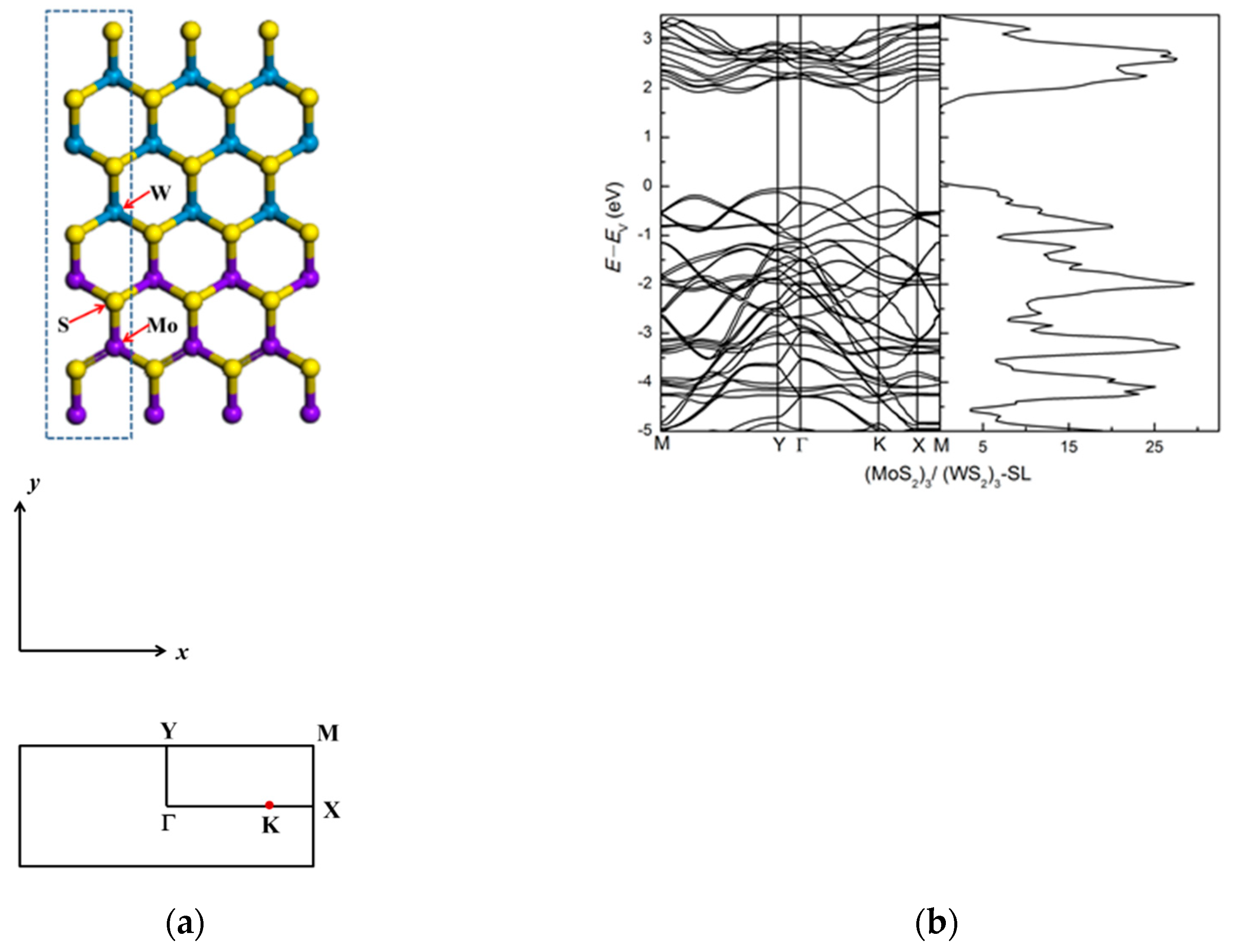
3.1.1. (MoS2)3/(WS2)3 Lateral Superlattice

We modeled a lateral superlattice (SL) as an artificially periodic system, with a unit cell normal to the monolayer containing a vacuum region of 12 Å. We first optimized the MoS2 and WS2 monolayer systems, obtaining the equilibrium lattice constant of 3.186 Å for both. Our calculated direct bandgap of 1.71 eV for MoS2 and 1.82 eV for WS2 are in good agreement with reported experimental and theoretical results [12,15,26,32,34,52,53]. The similarity of lattice parameters and different band gaps is suitable to build superlattices. We focus on (MoS2)3/(WS2)3 lateral superlattice (SL), as shown in Figure 1a. The band structure, shown in Figure 1b, indicates that this superlattice is also semiconducting and has direct band gap close to that of monolayer MoS2: the band gap is 1.71 eV for the (MoS2)3/(WS2)3 lateral superlattice, with both the valence band maximum (VBM) and conduction band minimum (CBM) located at the high symmetry point K of the monolayer system. The energy bands close to VBM and CBM are relatively flat along ΓY and dispersive along ΓX. The states near the band gap at the high symmetry point K are mainly derived from the d orbital of Mo atom and the p orbital of S atom.

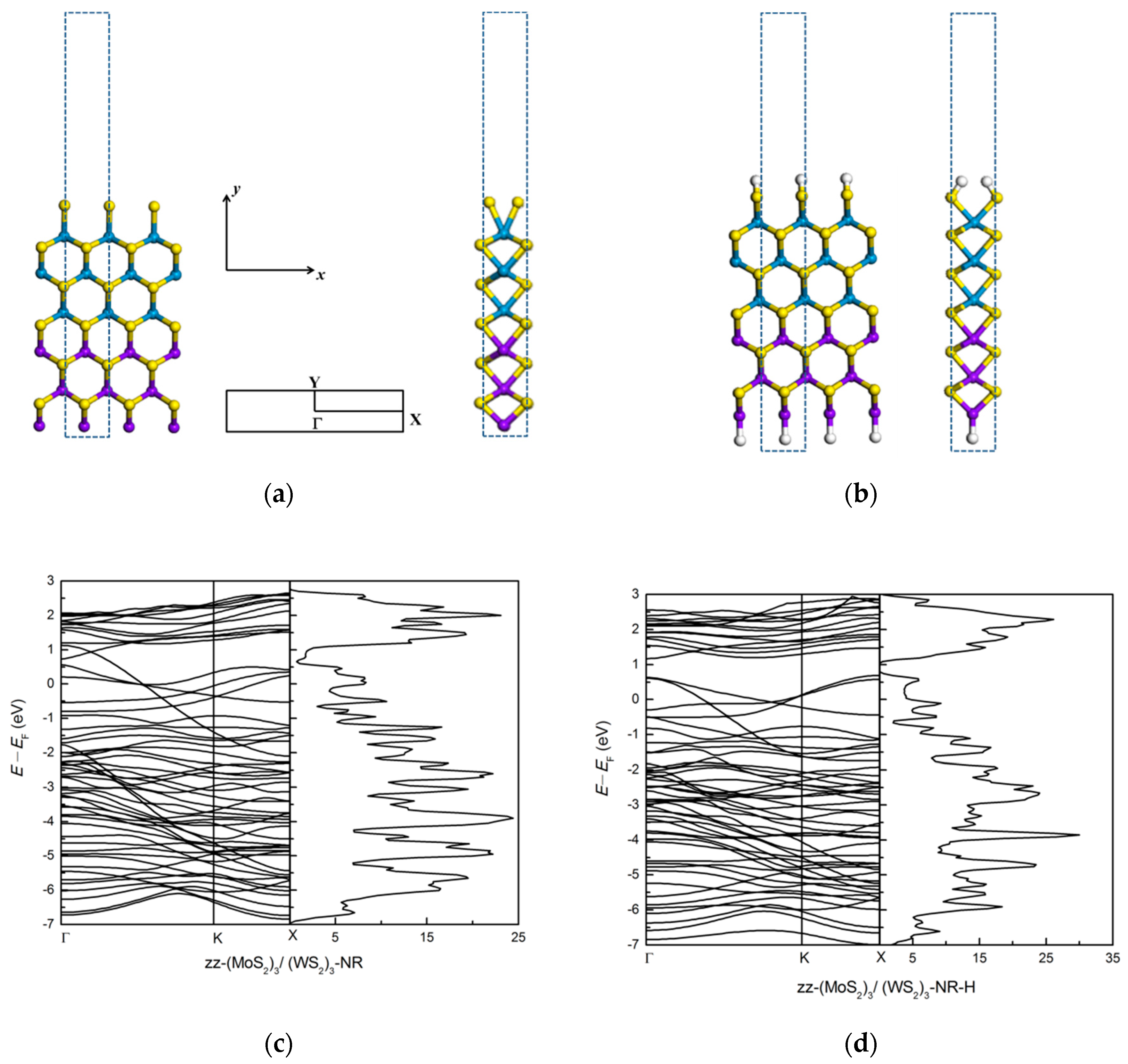
3.1.2. Zigzag (MoS2)3/(WS2)3 Lateral Nanoribbons

Nanoribbons were constructed by cutting the lateral (MoS2)3/(WS2)3 monolayer superlattice. There are zigzag (zz-NR) and armchair (ac-NR) nanoribbons with different chiralities and edge structures. As shown in Figure 2a, for zz-NR we used the rectangular unit as repeat unit cell of length a along x direction and (3 3 a plus a vacuum region of 12 Å) along y direction, where a is the lattice constant. There are 3 Mo, 3 W, 6 S atoms in the repeat unit.
The structural stability of a bare nanoribbon was examined by evaluating the edge energy per interface unit cell using the formula
Eedge = (Eribbonn1 × Eunit(MoS2) − n2 × Eunit(WS2) − nMo × E(Mo) − nW × E(W) − nS × E(S))/2L
Here Eribbon is the total energy of the nanoribbon unit cell, Eunit(MoS2) is the total energy of bulk MoS2 monolayer, Eunit(WS2) is the total energy of bulk WS2 monolayer, E(Mo) is is the total energy of bcc bulk Mo, E(W) is the total energy of bcc bulk W, we have considered E(S) as half of the total energy of a S2 molecule, n1 is the number of bulk MoS2 monolayers, n2 is the number of bulk WS2, nMo is the number of edge Mo atoms, nW is the number of edge W atoms, and nS is the number of edge S atoms, and L is the number of edge unit cells. For the zz-NR in Figure 2a the calculated edge energy is 0.89 eV. This result indicates that such a nanoribbon, terminated on one side by the metallic atom Mo and on the other side by the non-metallic atom S, is not a stable structure. Other zz-NR geometries can be constructed, as explained in [32], but we have not studied them all here. The study in [32] asserts that only S-terminated MoS2 zz-NR are stable geometries.
We also estimated the ‘’interface energy per interface unit cell’’ between the constituent materials of the superlattice nanoribbon (e.g., between MoS2 and WS2) by using the formula
EIF = Eedge − (EribbonnMoS2 × Eunit(MoS2) − nWS2 × Eunit(WS2))/2L
where nMoS2 and nWS2 are the numbers of MoS2 and WS2 units in the supercell used in any of the zigzag (zz-NR) and armchair (ac-NR) nanoribbons. For each of these structures, our computed interface energy is −2.27 eV, indicating that these interface formations are energetically favorable.
The structural stability of a passivated nanoribbon was examined by using the energy formula
Epassivation energy = (Epassivated ribbonEbare ribbonnH × E(H) − nX × E(X))/2L
where Epassivated ribbon is the total energy of the passivated ribbon, Ebare ribbon is the energy of the unpassivated (bare) ribbon, E(H) is taken as the half of the total energy of a H2 molecule, E(X) is half of the total energy of the X2 molecule, nH is the number of H atoms, and nX is the number of the X passivating atom. The passivation energy for the zz-NR structure in Figure 2b is −0.59 eV. This clearly suggests that this bare zz-NR in Figure 2a will become stable upon hydrogen passivation.
The high-symmetry points Γ, X and Y in Brillouin zone are marked. Due to lack of real periodicity along the y axis, the energy bands are flat along ΓY and we find dispersive bands along ΓX. As shown in Figure 2, we find that the zigzag (MoS2)3/(WS2)3 nanoribbon is a metal, similar to the results obtained in [32] for a MoS2 nanoribbon. Clearly, the H passivation of the zigzag (MoS2)3/(WS2)3 nanoribbon does not make the system semiconducting.

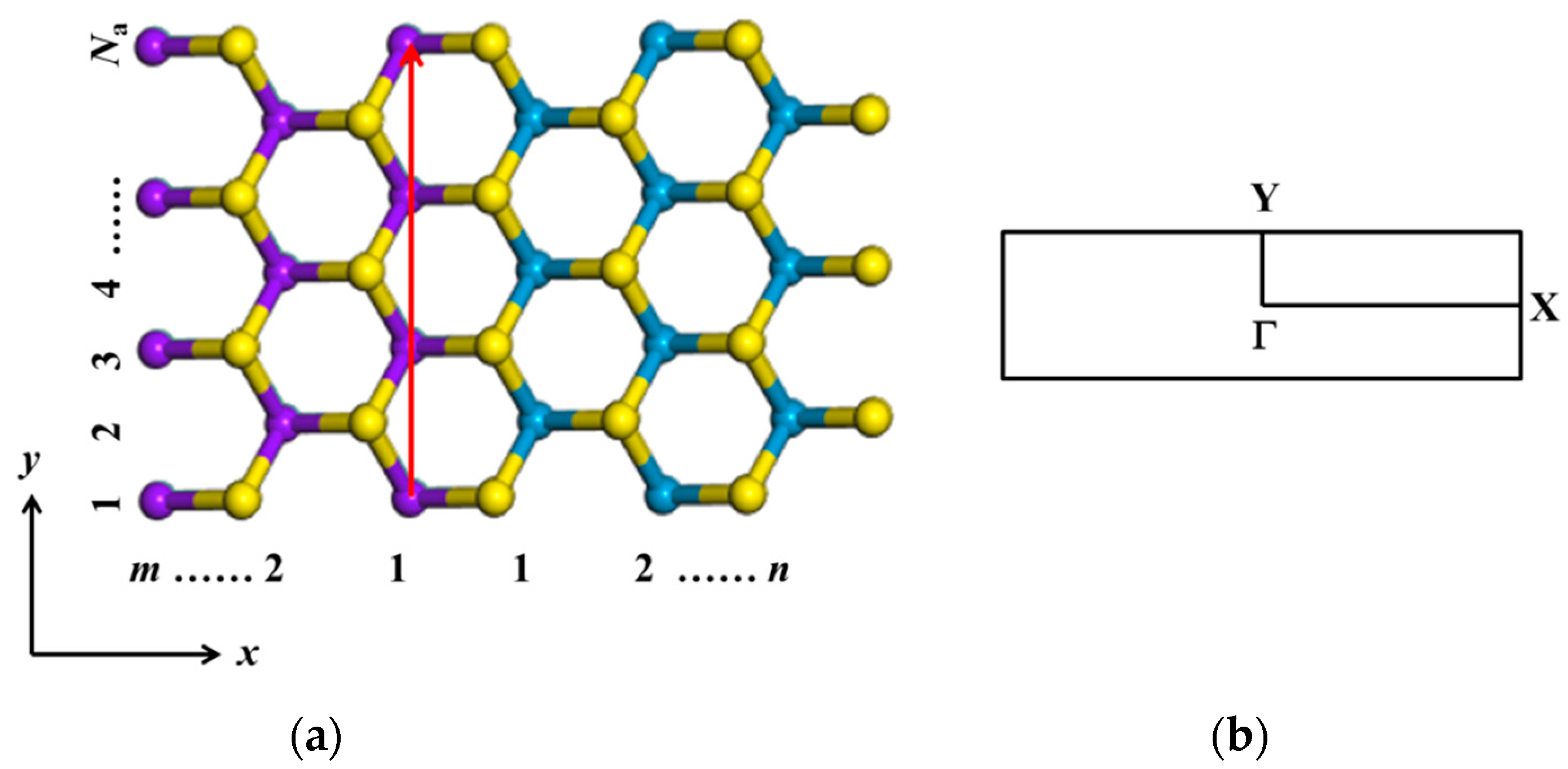
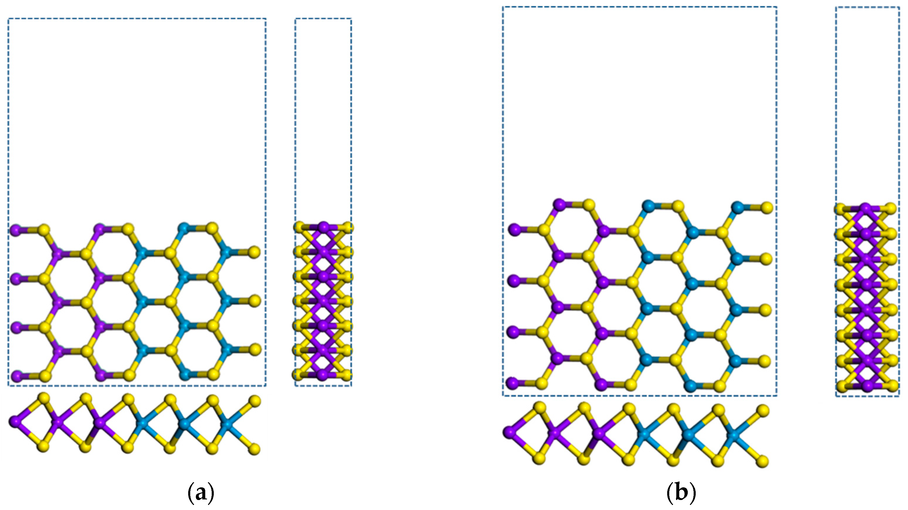
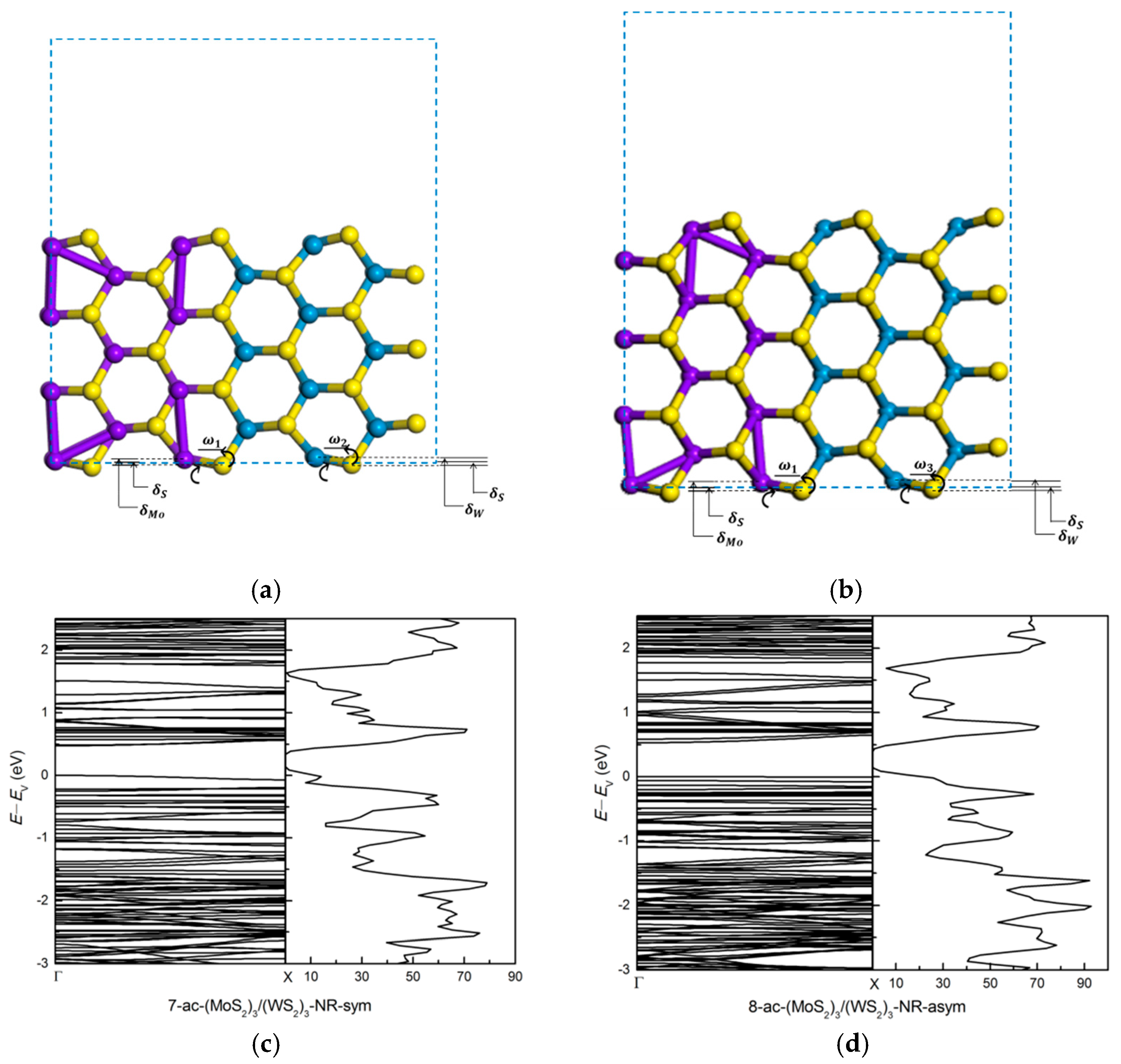
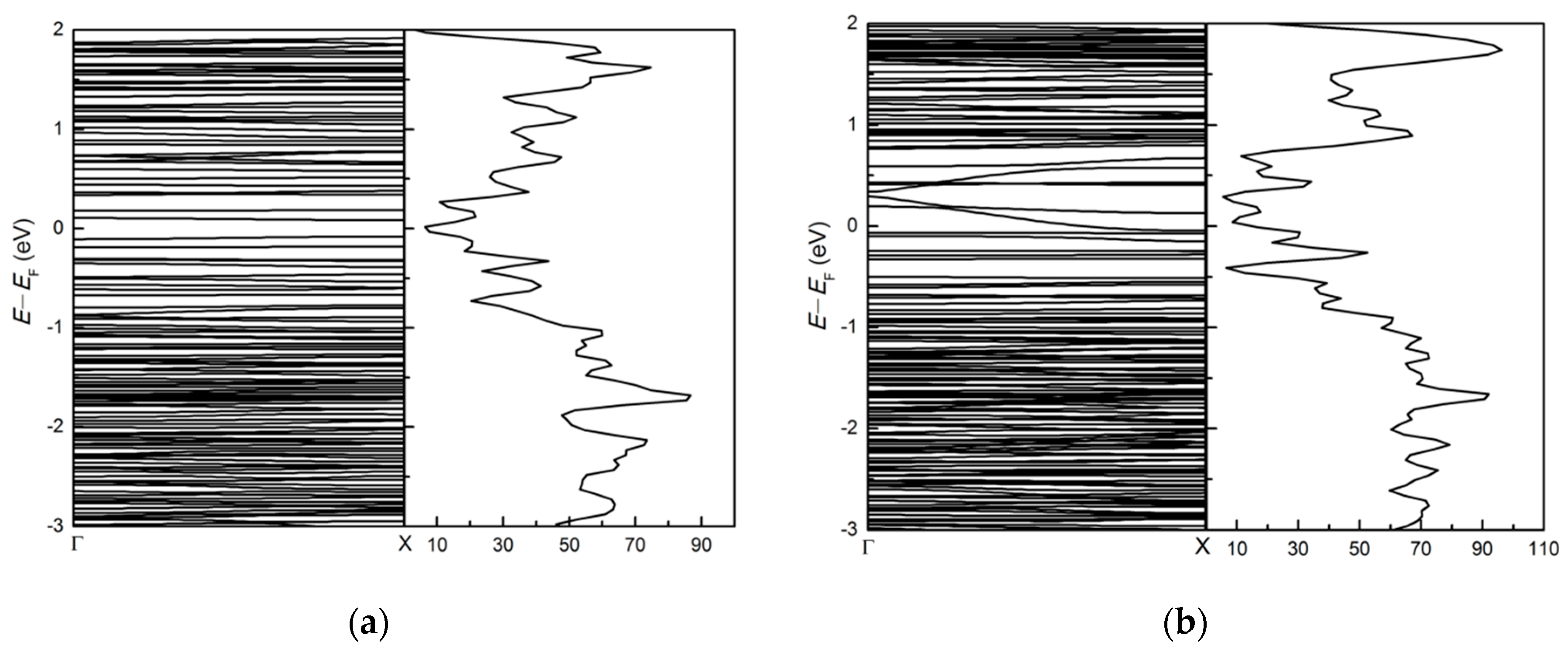
3.1.3. Armchair (MoS2)m/(WS2)n Lateral Nanoribbons

Figure 3 shows the structure of armchair MoS2-WS2 lateral superlattice nanoribbon. The vertical red arrow line marks the width of armchair nanoribbon. We use the notation Na-ac-(MoS2)m/(WS2)n-NR to describe a (MoS2)m/(WS2)n armchair nanoribbon. Here the width of the armchair nanoribbon is characterized by the number of atomic layers Na in the width direction. The numbers m and n denote the numbers of MoS2 and WS2 layers in the superlattice period. The x-axis is the superlattice period direction and the y-axis is the width direction. The high-symmetry points Γ, X and Y in the Brillouin zone are marked.
Both the symmetric and asymmetric armchair nanoribbons may lower their energy via formation of corrugation [33] or the bond reconstruction mechanism, as is widely realized for semiconductor surfaces, particularly the (001) surface of diamond structure materials and the (110) surface of zincblende materials [54]. However, in this work we have not considered any possible reconstructions of geometries discussed in the text.
In order to examine the effect of edge modification on the electronic properties we first focus on the m = n = 3 superlattice structure (MoS2)3/(WS2)3. Symmetric (7-ac-(MoS2)3/(WS2)3-NR-sym) and asymmetric (8-ac-(MoS2)3/(WS2)3-NR-asym) nanoribbon structures are constructed. Bare, and H-, H-S-, H-O-passivated nanoribbons are investigated, shown in Figure 4. The 7-ac-(MoS2)3/(WS2)3-NR-sym has an odd number of atomic layers and 8-ac-(MoS2)3/(WS2)3-NR-asym has an even number of layers. For the H-passivated nanoribbon we add two H atoms to the edge Mo or W atom and one H atom to the edge S atom. For the H-S- and H-O-passivated nanoribbons, we add one S or O atom to the edge Mo or W atom and one H atom to the edge S atom.
After atomic relaxation, the structure of zigzag nanoribbon does not change much. But the structure of armchair nanoribbons, both symmetric and asymmetric, has changed a lot. Compared to the S atoms, the Mo and W atoms on the edge shrink to the inside of the armchair nanoribbons, and the hexagonal ring structure is twisted and deformed, as shown in Figure 5a,b. The stability of a nanoribbon was examined by evaluating the edge energy formula in Equation (1). With Eedge(asym) = +0.03 eV the asymmetric structure in Figure 4b is unstable. In contrast, with Eedge(sym) = −0.26 eV the symmetric structure in Figure 4a is clearly stable. Our estimates of edge energy for these MoS2/WS2 superlattice nanoribbons are similar in trend, but different in estimate, compared to the finding in [32] for MoS2 armchair nanoribbons of different period and width than considered in this work.
In contrast to zigzag nanoribbons, armchair (MoS2)3/(WS2)3 nanoribbons exhibit semiconducting property. Semiconducting nature of armchair MoS2 nanoribbons were previously established in [32,34]. Figure 5c,d shows the bands and dos of bare sym and asym (MoS2)3/(WS2)3 armchair nanoribbon structures. The direct band gap of sym and asym structures is about 0.47 eV and 0.53 eV, respectively. These band gap values are much smaller than the band gap of the (MoS2)3/(WS2)3 superlattice presented earlier, which is caused by the formation of surface dangling bonds along the y axis. There is quite a lot of similarity and some dissimilarity between the band structures of the sym and asym nanoribbons. In particular, a few bands close to the top of the valence band (3 or 4 curves below EV) are flat for the asym structure. There are also flat bands for the sym structure, but these are further below EV. These differences are due to W and Mo being different chemical species.
Using Equation (3) we find that H passivation stabilizes the symmetric as well the asymmetric nanoribbon structures. The stabilizing energy upon H passivation is −8.84 eV and −9.15 eV for the symmetric and asymmetric structures, respectively. That is, the asymmetric structure becomes more stable than the symmetric structure by 0.31 eV. For H-S and H-O co-passivation the relative stability energies of the asymmetric structure over the symmetric structure are, respectively, 0.31 eV and 0.36 eV. Our estimates of the results for the thin MoS2/WS2 nanoribbon are somewhat higher than those for the asymmetric MoS2 nanoribbon of different period and width considered in [34]. Energy gain results in passivating the armchair nanoribbon by H, H and S, and H and O are listed in Table 1.
The bands and dos of H-, H-S-, H-O-passivated 7-ac-(MoS2)3/(WS2)3-NR-sym structures are shown in Supplementary Materials Figure S1a–c. The direct band gap of the bare structure is 0.47 eV, which changes respectively to 0.63, 1.12, and 1.43 eV upon H-, H-S-, and H-O-passivation. This shows that the edge atom passivation can adjust the band gap of the armchair nanoribbon. The H-passivation opens up the band gap, but only by a small amount. The H-S and H-O passivations result in higher energy band gaps. However, the H-S-passivated structure has indirect energy band gap. The bad gap is 1.43 eV for H-O- passivation, which is close to the value for monolayer MoS2. This is consistent with previous reports, for example H and O edge-terminated armchair MoS2 exhibits a direct band gap of about 1.43 eV in [34]. We find that there is some difference in unoccupied states for the H-, H-S- and H-O-passivated 7-ac-(MoS2)3/(WS2)3-NR-sym armchair nanoribbon structures. In particular, the states around 0.75 eV for the H-passivated system have been removed for the H-S- and H-O- systems. The peak above EV around 0.75 eV has a much bigger contribution from the d orbital of edge Mo and W atoms of H-passivated 7-ac-(MoS2)3/(WS2)3-NR-sym (in Supplementary Materials Figure S2), but there are no contributions from the d orbital of edge Mo and W atoms for the H-S- and H-O- systems in the same energy range above EV (in Supplementary Materials Figures S3 and S4).
The band structure and dos for H-, H-S-, H-O-passivated 8-ac-(MoS2)3/(WS2)3-NR-asym structures are shown in Supplementary Materials Figure S5. The direct energy band gap is 0.53 eV and 0.52 eV for bare and H-passivation anr-asym, respectively, again similar to the results in [34] which quotes the band gap values of 0.61 eV and 0.60 eV for the bare and H-passivated structures, repectively. The H-S-, H-O-passivations produce larger and indirect energy band gaps. The indirect energy band gap is 1.07 eV and 1.35 eV for H-S-, H-O-passivated anr-asym, respectively. As for the 8-ac-(MoS2)3/(WS2)3-NR-asym structure, the states around 0.7 eV for the H-passivated system have been removed for the H-S- and H-O- systems. The peak above EV around 0.7 eV has a much bigger contribution from the d orbital of edge Mo and W atoms of H-passivated 8-ac-(MoS2)3/(WS2)3-NR-asym (in Supplementary Materials Figure S6), but there are no contributions from the d orbital of edge Mo and W atoms for the H-S- and H-O- systems above EV around 0.7 eV (in Supplementary Materials Figures S7 and S8).

3.2. MoS2/MoTe2 System

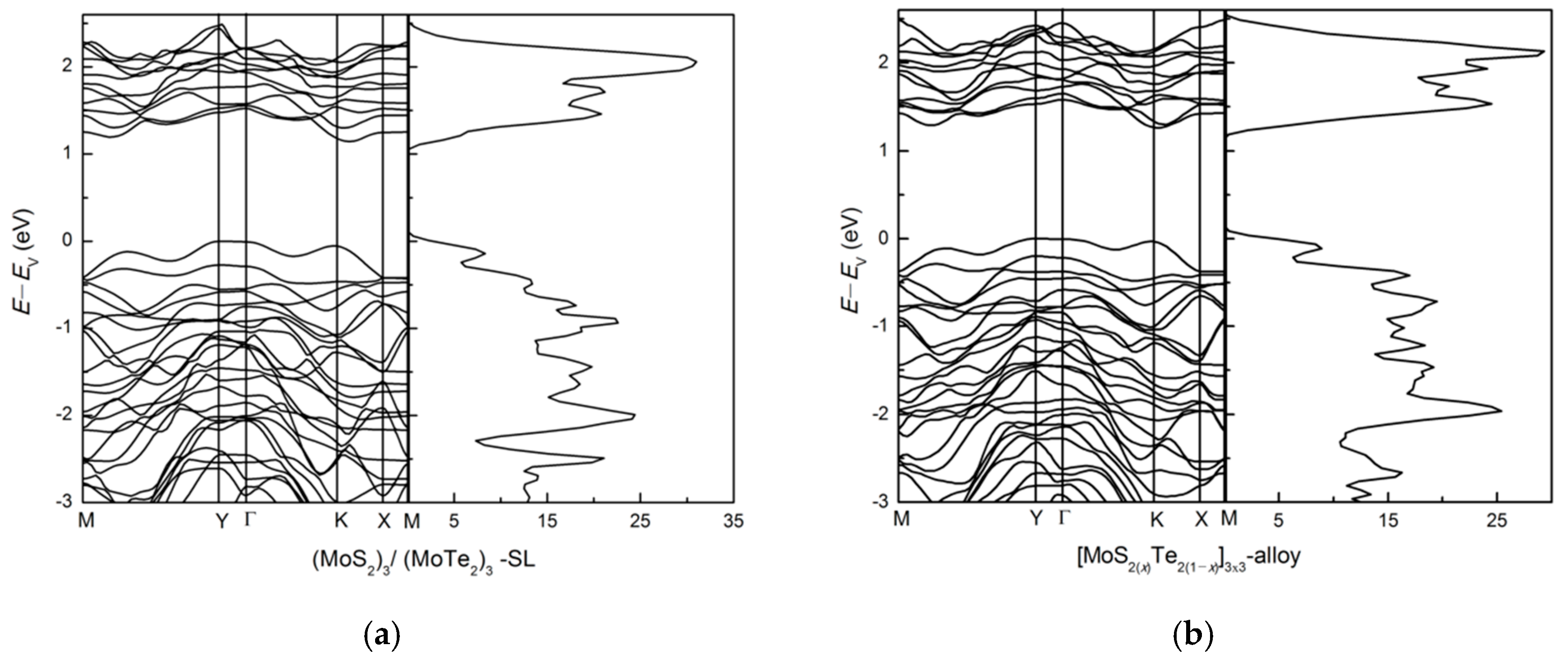
3.2.1. (MoS2)3/(MoTe2)3 Lateral Superlattice and Alloy

The (MoS2)3/(WS2)3 lateral superlattice and nanoribbon systems considered in the previous section contain two different cations: Mo and W. Because of the similarity in lattice constant and electronic structure of MoS2 and WS2 the superlattice and nanoribbon structures constructed from these do not exhibit any extraordinary features. In contrast, superlattice and nanoribbon structures using two TMDs with different anions, such as MoS2 and MoTe2, which have different lattice constants, are expected to exhibit pronounced features in their band structure.
To investigate such features, we first studied the band structure of the lateral superlattice (SL) as (MoS2)3/(MoTe2)3 and the alloy superlattice [MoS2(x)Te2(1−x)]3×3 (x = 0.5) using the same unit cell. The normal SL structure has the two bond lengths arranged periodically, whereas the alloy superlattice has the two bond lengths distributed randomly throughout the structure (we chose S and Te positions in a random manner). The total energy results show that the superlattice geometry (MoS2)3/(MoTe2)3 is energetically favorable and more stable than the separated constituents alloy geometry [MoS2(x)Te2(1−x)]3×3 (x = 0.5). The band structure and dos results are shown in Figure 6. The (MoS2)3/(MoTe2)3 superlattice is semiconductor with a band gap of 1.14 eV, close to that of monolayer MoTe2 (1.16 eV). The band gap of [MoS2(x)Te2(1−x)]3×3 (x = 0.5) is 1.26 eV, larger than that of the (MoS2)3/(MoTe2)3 superlattice. After alloying, the band edge of CBM is slightly increased, so that the band gap increases about 0.12 eV. The energy band near VBM is relatively flat along ΓY and dispersive along ΓX. Due to different bond length distributions there are some differences in the band structure for the two systems. The alloy superlattice has a slightly larger band gap and its energy bands show splitting at symmetry points, notably at the zone center Γ.

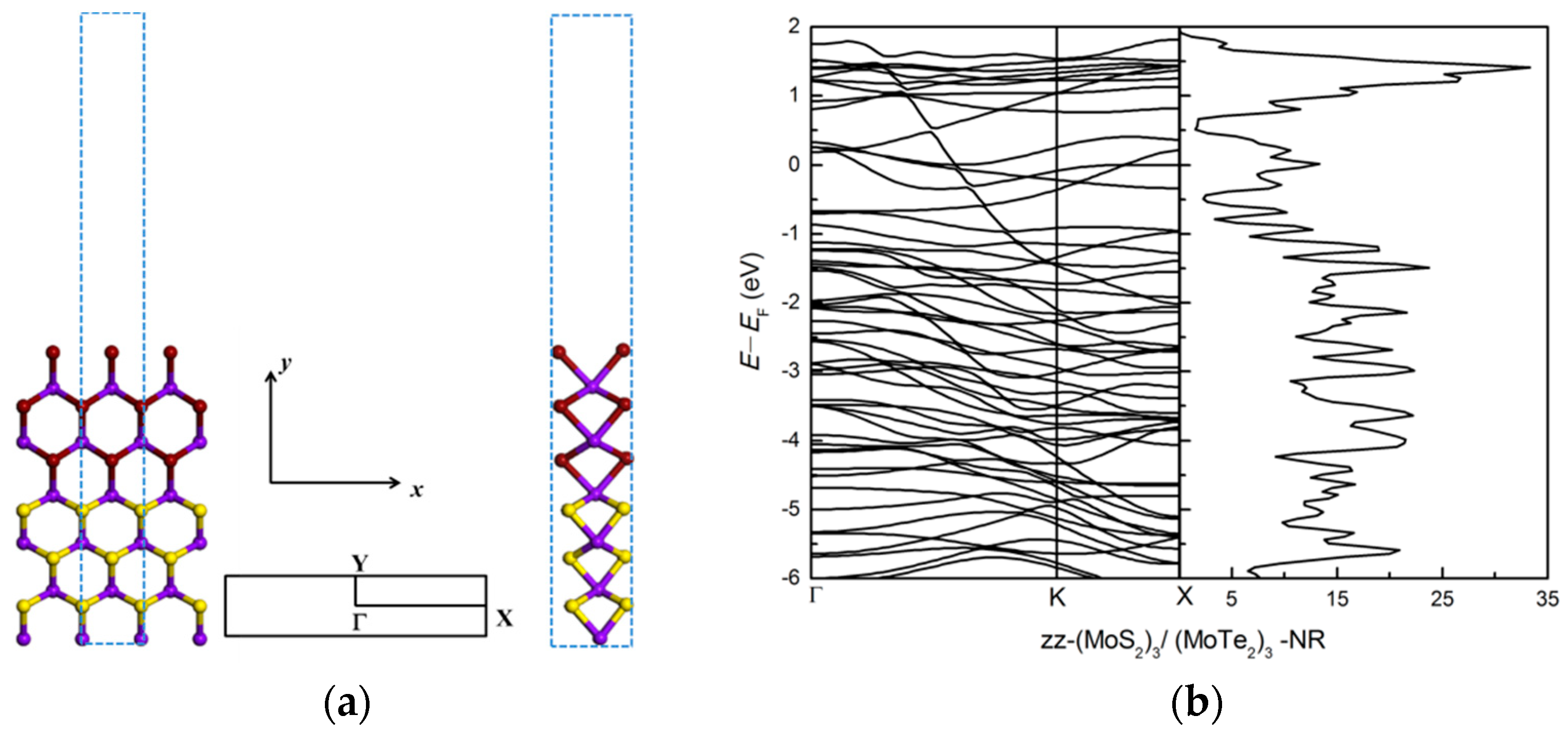
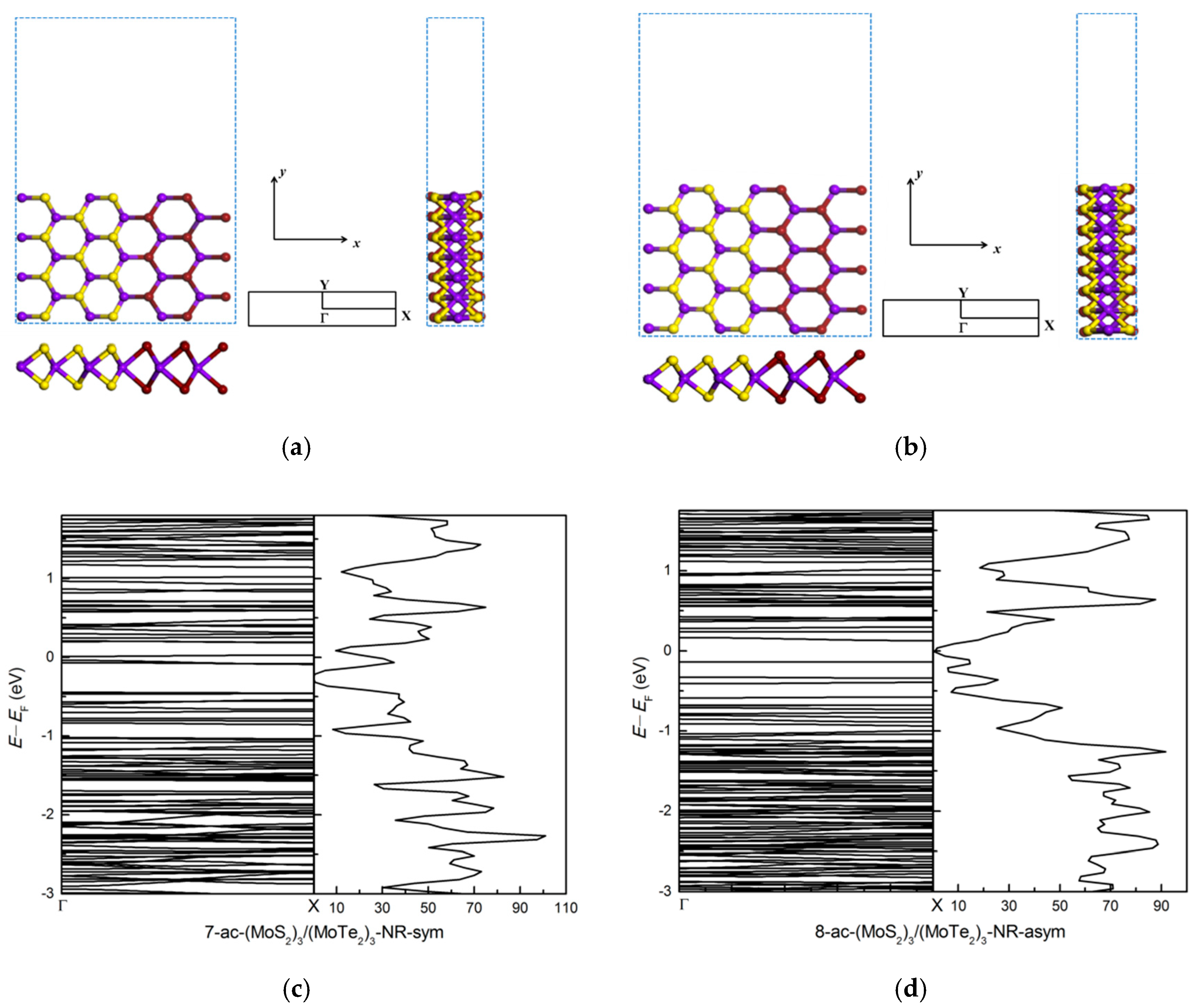
3.2.2. Zigzag and Armchair (MoS2)3/(MoTe2)3 Lateral Nanoribbons

Zigzag and armchair (MoS2)3/(MoTe2)3 lateral nanoribbons are investigated, with results shown in Figure 7 and Figure 8. After atomic relaxation, the structure of zigzag nanoribbon does not change much. But the structure of armchair nanoribbons has greatly changed. At the edge, compared to the anionic S atoms, the cationic Mo atoms move towards the ribbon and the anionic Te atoms move away from the ribbon, and the hexagonal ring structure is twisted and deformed. The Te atoms relax more than the S atoms.
The zigzag (MoS2)3/(MoTe2)3 nanoribbon is a metal (see Figure 7), similar to the zigzag (MoS2)3/(WS2)3 nanoribbon. However, in contrast to the zigzag (MoS2)3/(WS2)3 nanoribbon, the zigzag (MoS2)3/(MoTe2)3 nanoribbon is stable, with edge energy of −3.09 eV. The H-passivation energy is −0.34 eV.
The armchair (MoS2)3/(MoTe2)3 ribbon is stable in both symmetric and asymmetric structures, with edge energies, respectively, of −1.89 and −2.70 eV per edge atom. As shown in Table 1, the symmetric structure becomes more stable upon passivation, with energies, for H-, H-S and H-O passivations, of −8.48, −1.72 and −3.24 eV. The corresponding values for the asymmetric structure are −8.26, −1.50 and −3.10 eV.
The interface energy between the MoS2 and MoTe2 parts, using equation (2), is −5.89 eV, −3.48 eV and −4.08 eV for the zigzag (Figure 7a), symmetric armchair (Figure 8a) and asymmetric armchair (Figure 8b) structures, respectively. It is interesting that for the MoS2/MoTe2 nanoribbon system the interface energy shows large structural dependence, while we did not find any noticeable difference for different structures of the MoS2/WS2 nanoribbons. These differences are due to different amounts of the atomic relaxation at the interface and edges for the three types of nanoribbon structures considered here (see Table 2).
For the armchair (MoS2)3/(MoTe2)3 ribbon structure the edge Te atoms relax much more than the S atoms for the armchair (MoS2)3/(WS2)3 ribbon structure, as shown in Figure 5 and Figure 9. Following the practice adopted for semiconductor surface relaxation [54], we show in Table 2 the vertical displacements δ M o , δ W , δ S , δ T e and the tilt angles ω1 (for Mo-S bond), ω2 (for W-S bond), ω3 (for Mo-Te bond) for symmetric, asymmetric (MoS2)3/(WS2)3 and (MoS2)3/(MoTe2)3 armchair nanoribbons. There is larger vertical displacement for Mo, S, Te atoms for the (MoS2)3/(MoTe2)3 armchair nanoribbon than for Mo, W, S atoms in the (MoS2)3/(WS2)3 armchair nanoribbon. Especially Te atoms and Mo atoms connected to Te have large vertical displacements. Large vertical displacements lead to large tilt angles of about 48° and 50° for the Mo-Te bond in the symmetric and asymmetric structures, respectively. Structural changes cause changes in the band structure and electronic properties. This results in large reduction in the band gap upon (MoS2)3/(MoTe2)3 ribbon formation. Figure 8 shows the bands and dos of bare symmetric (7-ac-(MoS2)3/(MoTe2)3-NR-sym) and asymmetric (8-ac-(MoS2)3/(MoTe2)3-NR-asym) armchair nanoribbon structures. Both the 7-ac-(MoS2)3/(MoTe2)3-NR-sym and 8-ac-(MoS2)3/(MoTe2)3-NR-asym systems show metallic nature. This is different from 7-ac-(MoS2)3/(WS2)3-NR-sym and 8-ac-(MoS2)3/(WS2)3-NR-asym, which are semiconductors with band gaps of 0.47 eV for sym and 0.53 eV for asym structure.
The metallic bare symmetric armchair nanoribbon 7-ac-(MoS2)3/(MoTe2)3-NR-sym is acquires band gaps of 0.60, 0.90, and 0.76 eV for H-, H-S-, H-O-passivations, respectively, as shown in Figure 10. The H-passivated structure has direct energy band gap, but the H-S-, H-O-passivated structures have indirect energy band gap. The H-, H-S-, H-O-passivated structure opens up the band gap. The H-S-passivation produces the highest energy band gap, which is different from the (MoS2)3/(WS2)3 system. The unoccupied states of H-passivated structure are different from H-S- and H-O-passivated structures. The states around 0.75 eV for the H-passivated system decrease for H-O-passivated system and have been removed for the H-S- passivated systems. The peak above EV around 0.75 eV has a much bigger contribution from the d orbital of edge Mo atoms of H-passivated 7-ac-(MoS2)3/(MoTe2)3-NR-sym, but there are no contributions from the d orbital of edge Mo atoms for the H-S- systems in the same energy range above EV.
The metallic bare asymmetric MoS2/MoTe2 armchair nanoribbon (8-ac-(MoS2)3/(MoTe2)3-NR-asym) acquires band gap values of 0.46, 0.81, and 0.98 eV for H-, H-S-, H-O-passivated asymmetric MoS2/MoTe2 armchair nanoribbon, respectively, as shown in Figure 11. The H-passivation structure has direct energy band gap. The H-S-, H-O-passivation structure has indirect energy band gap. The gap opens up for the H-, H-S-, H-O-passivated structures. The H-O-passivation produces the highest energy band gaps, similar to the (MoS2)3/(WS2)3 system. As for the 8-ac-(MoS2)3/(MoTe2)3-NR-asym structure, the states around 0.6 eV for the H-passivated system have been removed for the H-S- and H-O- systems. The peak above EV around 0.6 eV has a much bigger contribution from the d orbital of edge Mo atoms of H-passivated 8-ac-(MoS2)3/(MoTe2)3-NR-asym, but there are no contributions from the d orbital of edge Mo atoms for the H-S- and H-O- systems above EV around 0.6 eV.

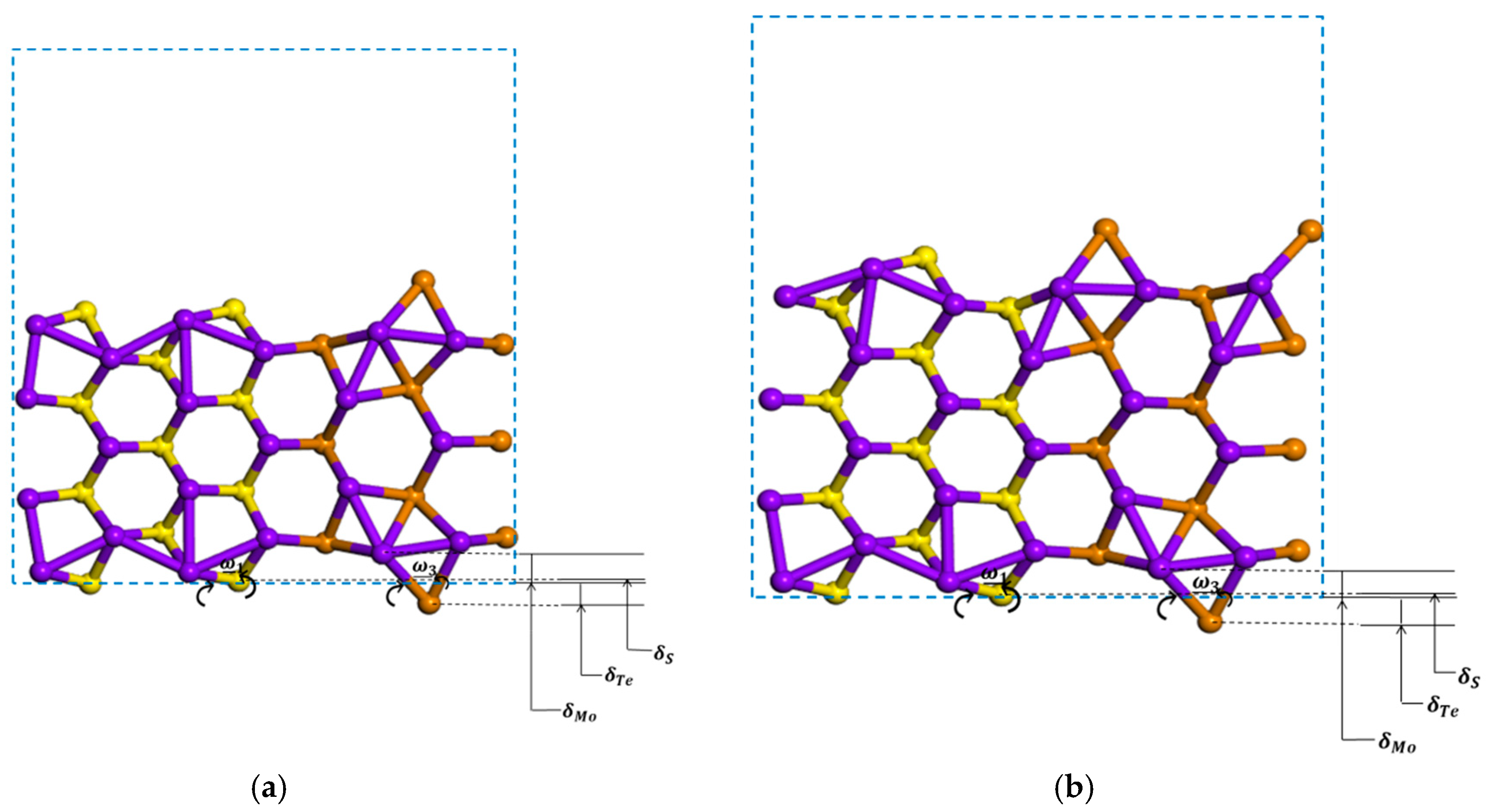
3.2.3. Symmetric and Asymmetric MoS2(x)Te2(1−x) Alloy (x = 0.5) Armchair Nanoribbons

The alloy has the two bond lengths Mo-S and Mo-Te distributed randomly throughout the structure (we chose S and Te positions in a random manner). Compared to bare symmetric and asymmetric (MoS2)3/(MoTe2)3 armchair nanoribbons, the asymmetric MoS2(x)Te2(1−x) alloy (x = 0.5) armchair nanoribbon and the symmetric MoS2(x)Te2(1−x) alloy (x = 0.5) armchair nanoribbon are still metallic. The results are shown in Figure 12. After alloying, the band edge of CBM of symmetric MoS2(x)Te2(1−x) alloy (x = 0.5) armchair nanoribbon (in Figure 12a) is slightly increased than that of symmetric (MoS2)3/(MoTe2)3 armchair nanoribbon (in Figure 8c). Due to different bond length distributions, there are some differences in the band structure for the two systems.

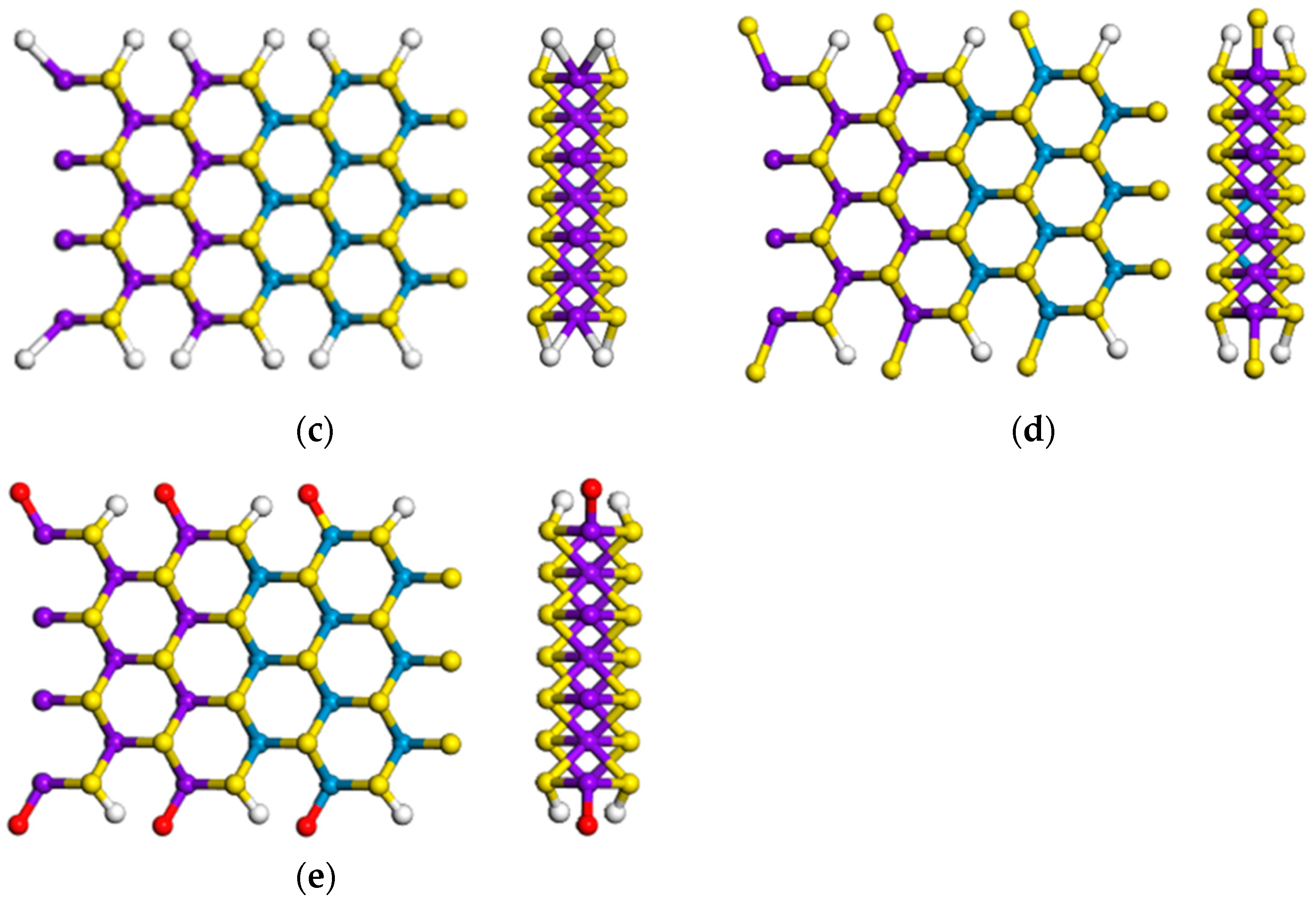
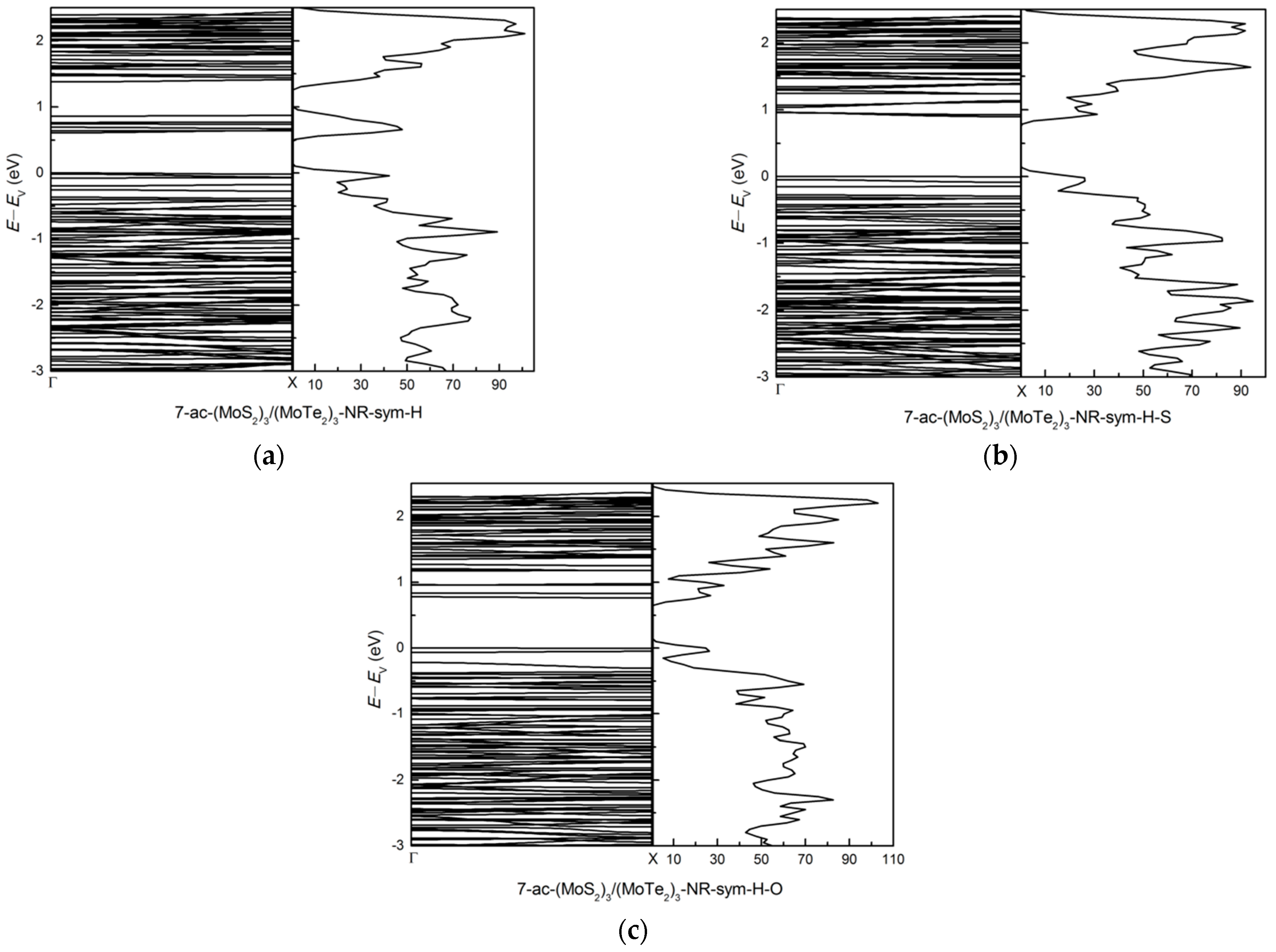
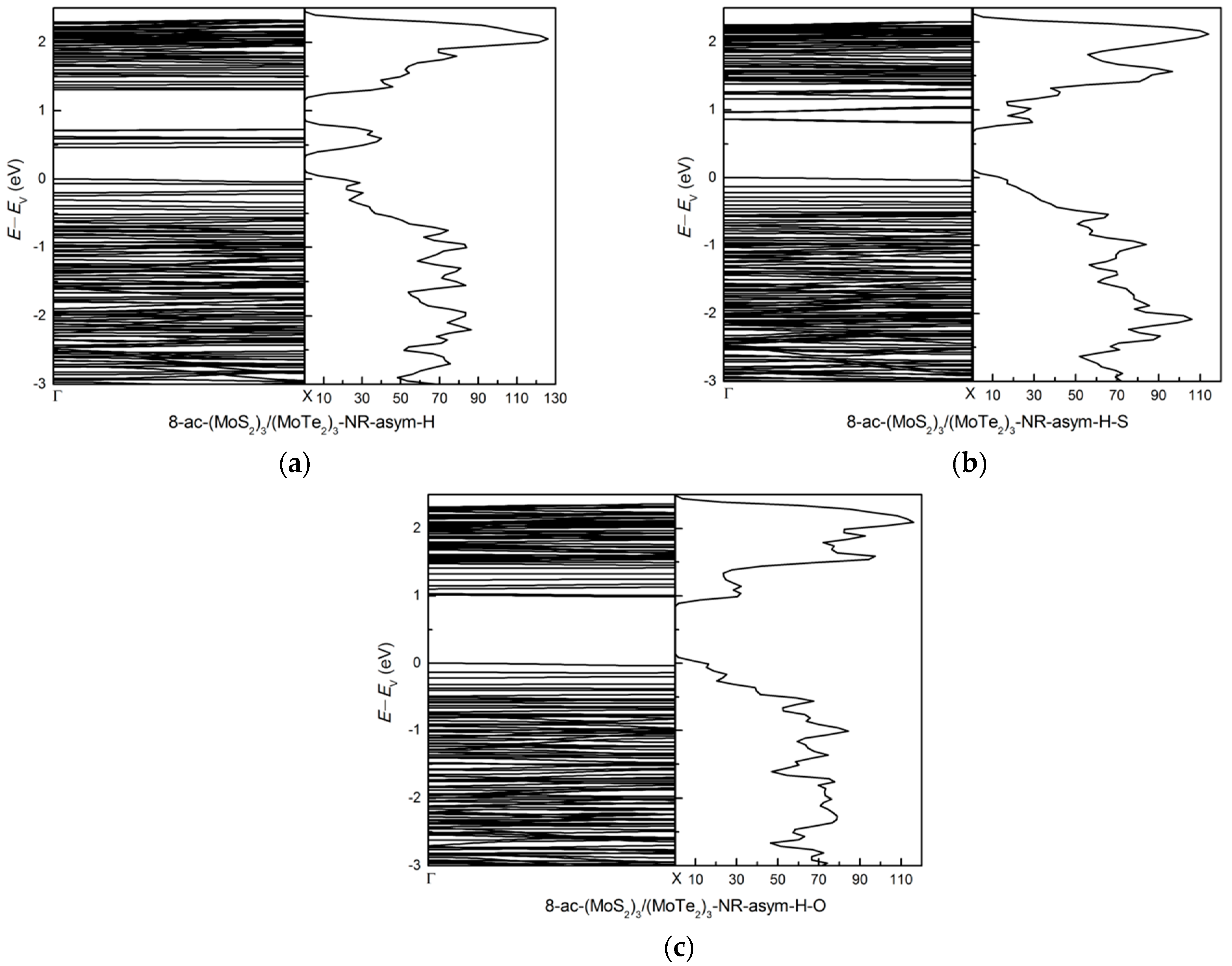
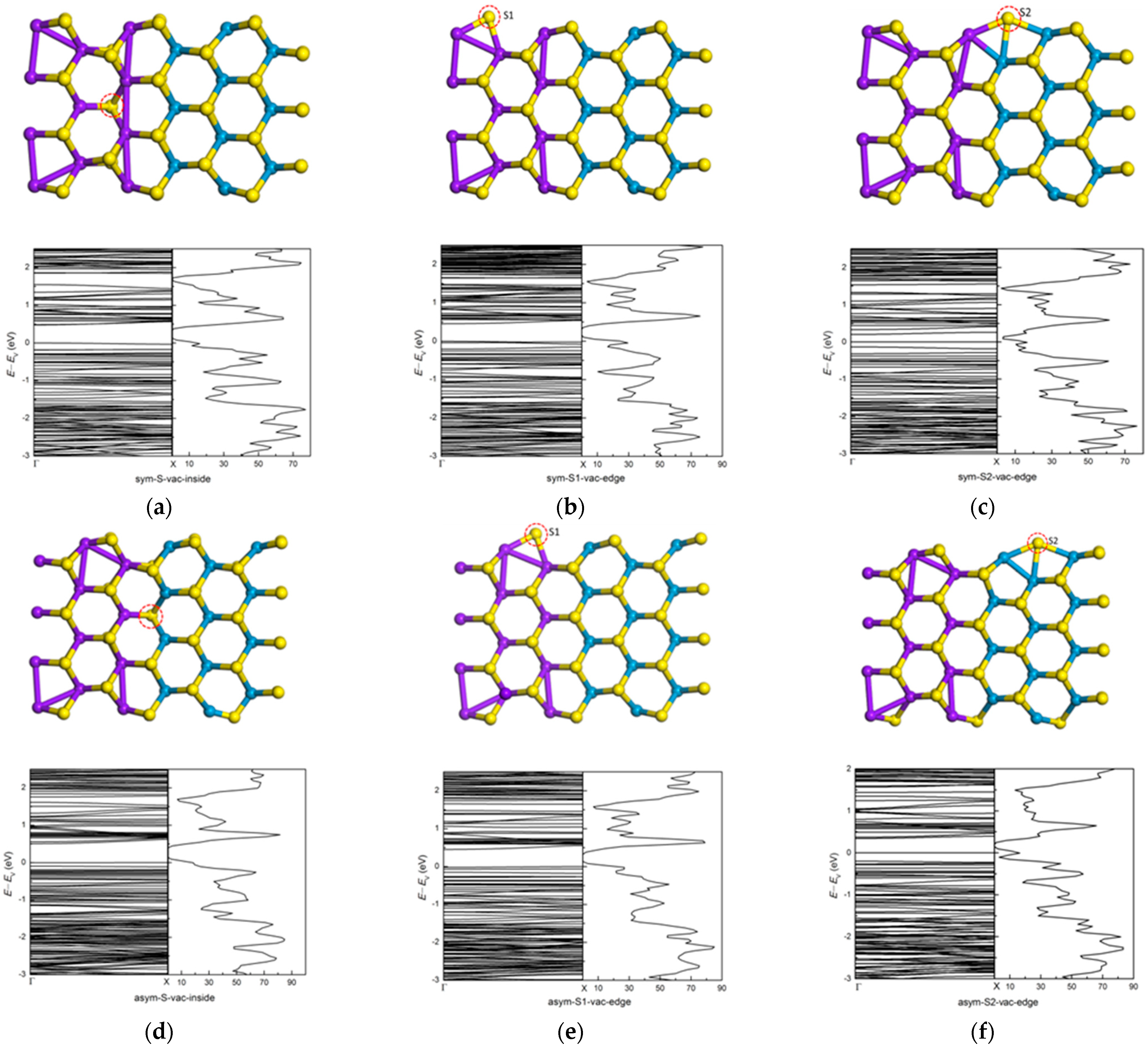
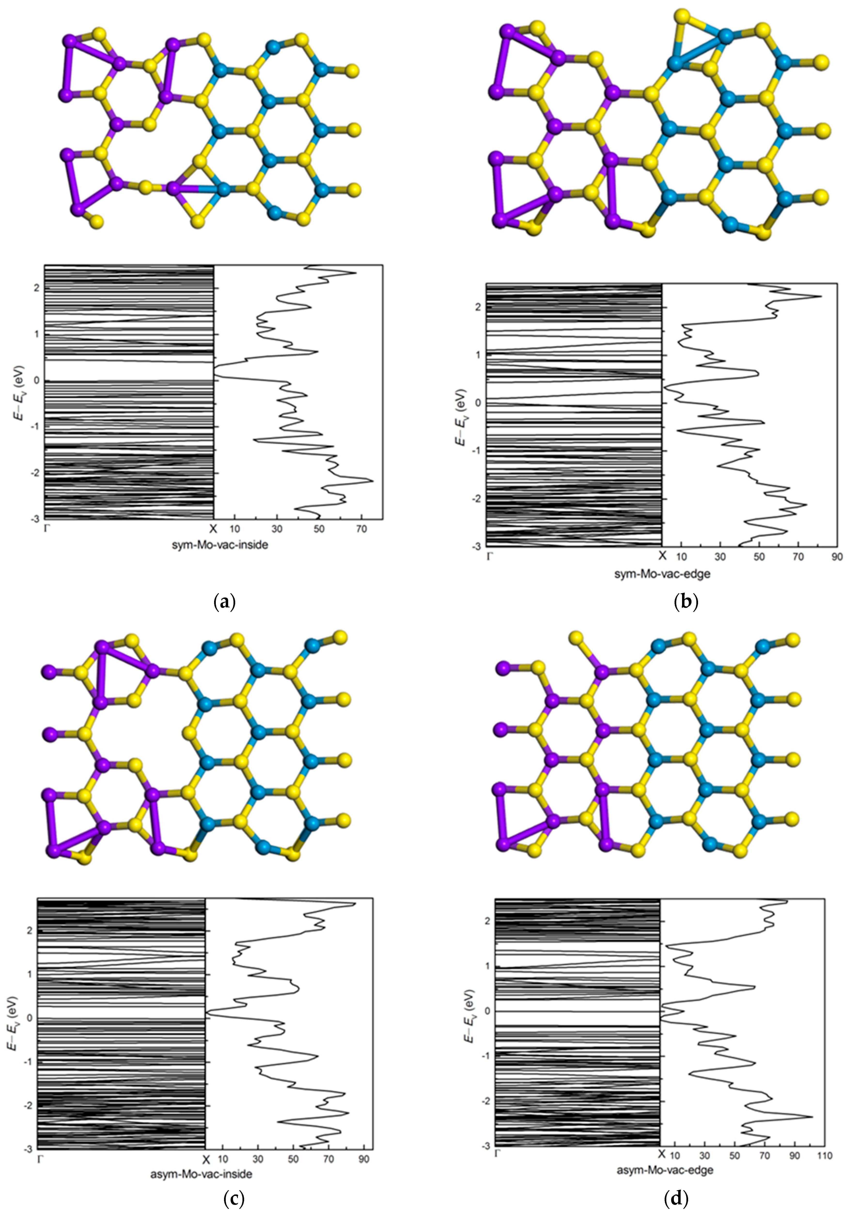
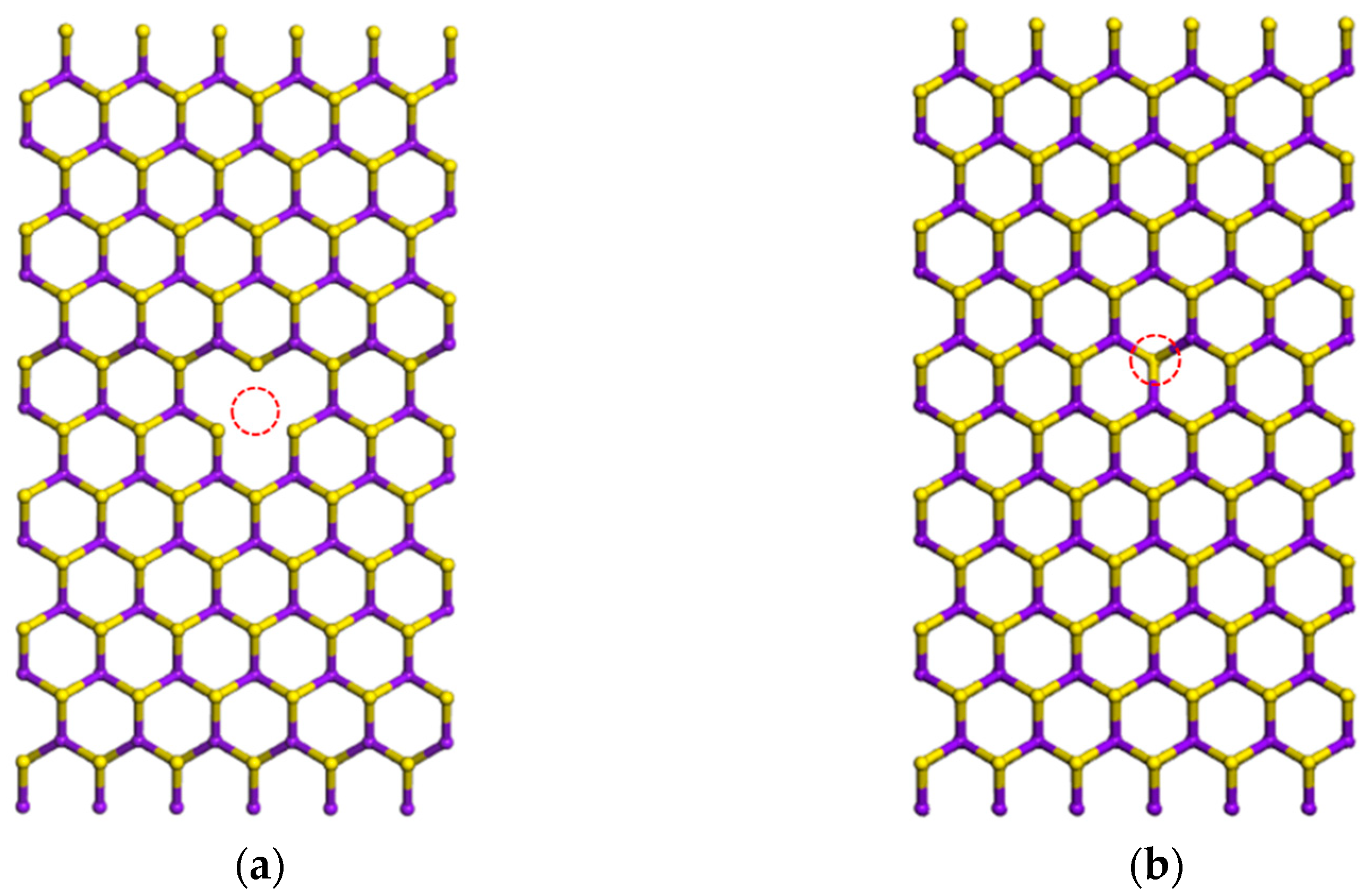
3.3. Effects of Atomic Vacancies in (MoS2)3/(WS2)3 Armchair Nanoribbon

Point defects in a material play an important role in its physical properties. For two-dimensional materials, defects, such as impurities and vacancies, can cause local deformation and stress and have impact on their electronic, magnetic and transportation properties [27,55,56,57,58]. We consider two cases: (1) a vacancy inside the ribbon and (2) a vacancy at the ribbon edge. There is also significant difference between sym and asym structures. Figure 13 shows the bands and dos of symmetric (7-ac-(MoS2)3/(WS2)3-NR-sym) and asymmetric (8-ac-(MoS2)3/(WS2)3-NR-asym) armchair nanoribbons with an interior and an edge S vacancy. Among the edge defects, one is the defect of S connected to Mo atom (S1), and the other is the defect of S connected to W atom (S2). The edge S2 vacancy both in the symmetric and asymmetric nanoribbon produces a much-reduced band gap. The band gap is 0.48 eV and 0.46 eV for inside S vacancy and edge S1 vacancy in the symmetric (MoS2)3/(WS2)3 armchair nanoribbon, which is similar to bare symmetric (MoS2)3/(WS2)3 armchair nanoribbon (0.47 eV). We can find similar bands and dos characters around the CBM and VBM with bare symmetric (MoS2)3/(WS2)3 armchair nanoribbon. The edge S2 vacancy in the symmetric (MoS2)3/(WS2)3 armchair nanoribbon reduces the band gap from 0.47 eV to 0.20 eV. For both inside and edge S1 vacancies in the asymmetric (MoS2)3/(WS2)3 armchair nanoribbon, the band gap only changes a little, being 0.51 eV and 0.45 eV, respectively. The edge S2 vacancy in the asymmetric (MoS2)3/(WS2)3 armchair nanoribbon reduces the band gap from 0.53 eV to 0.34 eV. The bands and dos change a lot. There are new energy levels in the band gap region. The peak around EV comes from the contribution of the d orbitals Mo and W atoms at the edges around the defect.
Figure 14 shows the bands and dos of symmetric (7-ac-(MoS2)3/(WS2)3-NR-sym) and asymmetric (8-ac-(MoS2)3/(WS2)3-NR-asym) armchair nanoribbons with inside and edge Mo vacancy. There is a clear difference in the band gap states between inside and edge Mo vacancy for symmetric structure, while there is only a little difference for asymmetric structure, inside and edge Mo vacancy both reduce the band gap. The band gap for inside Mo vacancy in symmetric (MoS2)3/(WS2)3 armchair nanoribbons is 0.40 eV. The p orbital of S atom and d orbital of Mo atoms around Mo vacancy have more contribution below the EV. The edge Mo vacancy in symmetric (MoS2)3/(WS2)3 armchair nanoribbons changes the band gap from 0.47 eV to 0.10 eV. The p orbital of S atom around Mo vacancy has more contribution below the EV than that of bare symmetric (MoS2)3/(WS2)3 armchair nanoribbon. Inside and edge Mo vacancies in asymmetric (MoS2)3/(WS2)3 armchair nanoribbons both change the band gap: the value decreases to 0.27 eV and 0.26 eV, respectively. There are new energy levels around 0.28 eV and 0.35 eV for inside Mo vacancies in asymmetric (MoS2)3/(WS2)3 armchair nanoribbon. The peak comes from the contribution of the p orbitals of S atoms around the Mo defect. The new energy level around EV mainly comes from the contribution of the d orbitals of edge W atom, and there is less contribution the p orbitals of the S atoms around the Mo defect.
There is strong vacancy-vacancy interaction in the thin-period nanoribbons considered above. In order to get a realistic understanding of the role of a single vacancy for band gap changes, we made bulk vacancy calculations using a large unit cell for MoS2 including 216 atoms. We created a Mo vacancy (or S vacancy) somewhere in the middle of the unit cell, as shown in Figure 15a,b. Vacancies in neighboring unit cells will be ’reasonably far’ to interact and we get vacancy related flat electronic bands inside the bulk band gap, and pdos will allow us to find out the chemical and orbital signature of that band. For Mo vacancy, impurity energy levels around 0.00 eV, 0.35 eV, 0.73 eV are found to be located near the valence band maximum (VBM) and exhibit strong local characteristics, shown in Supplementary Materials Figure S9. The energy levels at 0.00 eV and 0.35 eV are doubly degenerate. The valance band maximum (VBM) level comes from the p orbital of S atoms around Mo vacancy. The bottom of the conduction (CBM) level mainly comes from d orbitals of Mo atoms and a small part is composed of the p orbitals of S atoms. Thus, the impurity energy levels come from the d orbitals of Mo atoms and p orbitals of S atoms around the Mo vacancy (see Supplementary Materials Figure S10). For S vacancy, there is a doubly degenerate impurity energy level around 1.26 eV, shown in Supplementary Materials Figure S11. This impurity energy level comes from the d orbitals of Mo atoms around the S vacancy (see Supplementary Materials Figure S12).

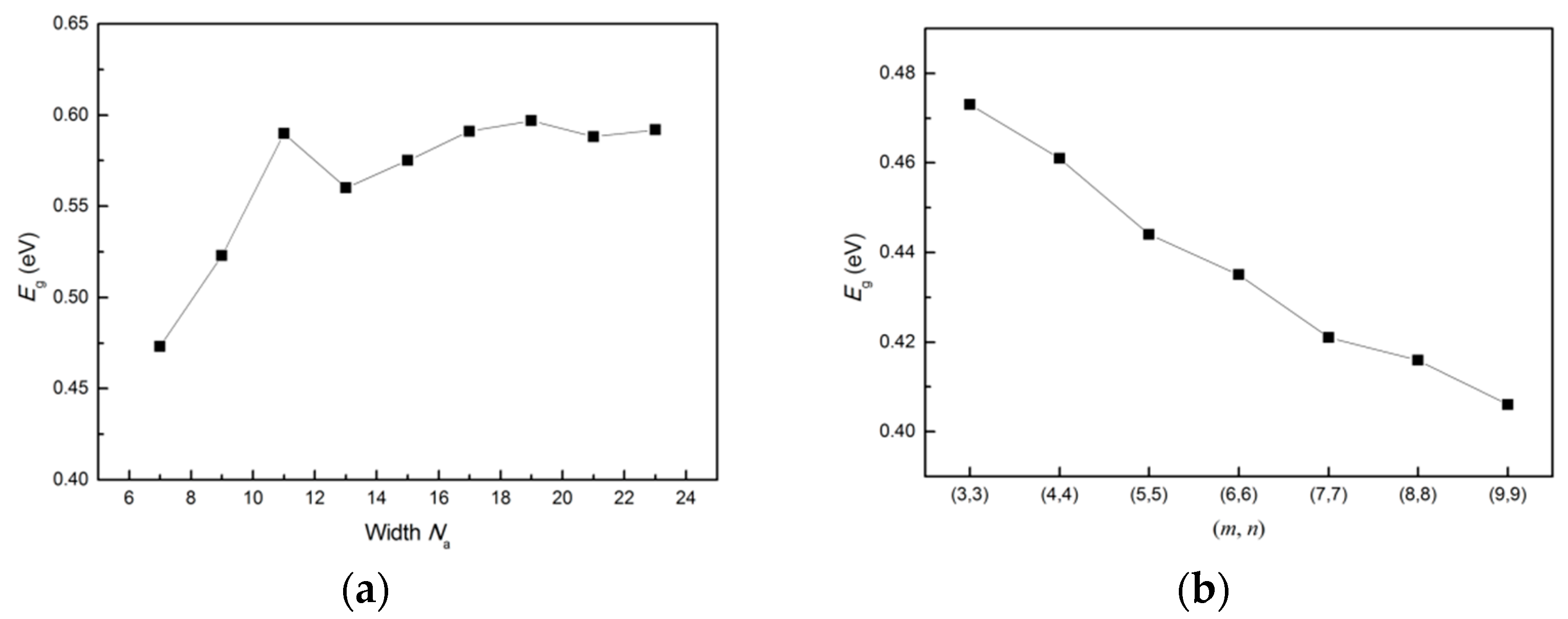
3.4. Band Gap Variation with Ribbon Width and Period

We now investigate how the band gap changes as we fix the period size and change the width for the armchair (MoS2)m(WS2)n lateral nanoribbon. We change the width Na from 7 to 23 and obtain the relation between band gap and width as shown in Figure 16a. The band gap is oscillating as we increase the width and fix the period as (m, n) = (3, 3), and finally converges to a value about 0.59 eV, which are in agreement with the previous calculations for the armchair MoS2 and WS2 nanoribbons in [26,27,28,30,59]. Similarly, we investigate how the gap changes as we fix the width and change the period. With change in the superlattice period (m, n), the relationship between the band gap and superlattice period is shown in Figure 16b. It is not the same as increasing the width, as the band gap decreases with increasing superlattice period. This is due to reduction in the confinement effect with increase in period size from (m, n) = (3, 3) until (m, n) = (9, 9).

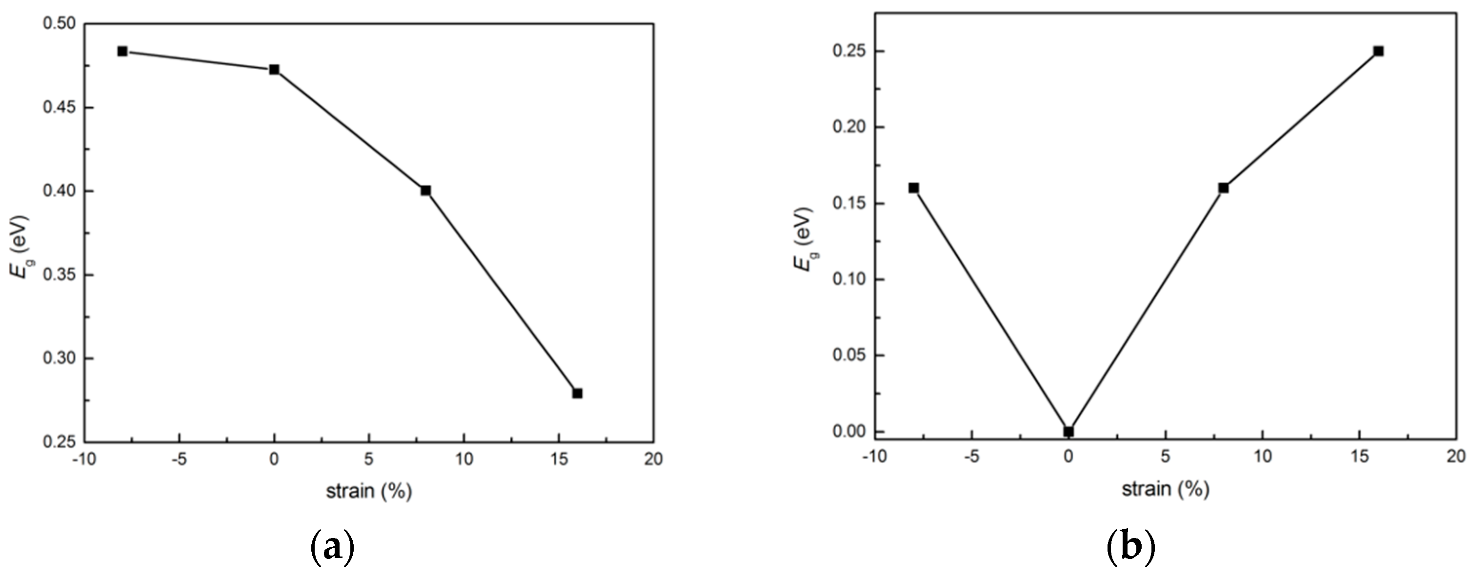
3.5. Bang Gap Variation with Biaxial Strain

Application of strain can tune electronic properties of materials. We examine the effect of biaxial strain on the band gap of the nanoribbons. The electronic band structures of 7-ac-(MoS2)3/(WS2)3-NR-sym, 7-ac-(MoS2)3/(MoTe2)3-NR-sym armchair nanoribbons under tensile and compressive biaxial strain have been studied. We applied different values of biaxial strain by changing lattice constant. The band gap under strain is shown in Figure 17. The energy gap of 7-ac-(MoS2)3/(WS2)3-NR-sym increases under compressive strain and decreases under tensile strain, which is similar to the results obtained previously for monolayer MoS2 [42]. The energy gap of 7-ac-(MoS2)3/(MoTe2)3-NR-sym increases under both the compressive and tensile biaxial strains, which is different from the 7-ac-(MoS2)3/(MoTe2)3-NR-sym system. When the system is stretched or compressed, the relative position changes between the atoms, which affects the bonding properties and the coupling between different orbitals, so the band structure changes. The edge states play an important role in nanoribbon. The Te atom has a higher atomic number and lower electronegativity than the S atom. After atomic relaxation, the structures of 7-ac-(MoS2)3/(WS2)3-NR-sym and 7-ac-(MoS2)3/(MoTe2)3-NR-sym are very different, especially at the edge of the nanoribbon as discussed earlier, resulting in a big difference in the band structure with strain.

4. Conclusions

(MoS2)3/(WS2)3 and (MoS2)3/(MoTe2)3 lateral monolayer superlattices, and their zigzag and armchair nanoribbons were studied using DFT calculations. The structural, edge atom modification, vacancy effect and biaxial strain effect of (MoS2)3/(WS2)3 and (MoS2)3/(MoTe2)3 nanoribbons were investigated. The bare zig-zag and asymmetric (MoS2)3/(WS2)3 nanoribbons are unstable, but can be stabilized by H passivation. The bare symmetric (asymmetric) structure is found to be stable (unstable). Both the symmetric and asymmetric structures are stable when passivated by H atoms, or co-passivated by H and S, or by H and O atoms; however, the asymmetric structure is relatively more stable. In contrast to the (MoS2)3/(WS2)3 nanoribbons, zig-gag and armchair (MoS2)3/(MoTe2)3 nanoribbons are stable with or without passivation. Because of large lattice mismatch the band structure of (MoS2)3/(MoTe2)3 superlattice is quite different from that of (MoS2)3/(WS2)3. The band gaps open up when the (MoS2)3/(WS2)3 and (MoS2)3/(MoTe2)3 armchair nanoribbons are passivated by H, S and O atoms. In particular, (MoS2)3/(WS2)3 ANR-H-O exhibits a remarkably large band gap change. The band gap of the (MoS2)3/(WS2)3 nanoribbon oscillates as we increase the width and fix the period as (m, n) = (3, 3), and finally converges to a value about 0.59 eV. When we fix the width and change the period, the band gap decreases with increasing superlattice period. The band gap with the edge S vacancy connecting to the W atom is much smaller than the S vacancy connecting to the Mo atom. In contrast, inside and edge Mo vacancies both reduce the band gap. The electronic orbitals of atoms around the Mo vacancy play an important role in characterizing the VBM and CBM and impurity levels. Under tensile and compressive biaxial strain, the structures of 7-ac-(MoS2)3/(WS2)3-NR-sym and 7-ac-(MoS2)3/(MoTe2)3-NR-sym are very different, resulting in a big difference in the band structure with strain.

Supplementary Materials

The supplementary material contains the band structure, dos and pdos of H-, H-S- and H-O-passivated symmetric and asymmetric (MoS2)3/(MoTe2)3 armchair nanoribbons. The band structure, dos and pdos of MoS2 SL with a Mo or S vacancy in the middle. The following are available online at https://www.mdpi.com/2079-4991/11/2/534/s1, Figure S1: The band structure and dos: (a) 7-ac-(MoS2)3/(WS2)3-NR-sym-H, (b) 7-ac-(MoS2)3/(WS2)3-NR-sym-H-S and (c) 7-ac-(MoS2)3/(WS2)3-NR-sym-H-O, Figure S2: (a) The relaxed geometry of 7-ac-(MoS2)3/(WS2)3-NR-sym-H, edge and inside atoms for Mo and W are labeled. The partial density of states (pdos) for (b) inside Mo6 atom; (c) edge Mo10 atom; (d) edge Mo11 atom; (e) inside W15 atom; (f) edge W21 atom of 7-ac-(MoS2)3/(WS2)3-NR-sym-H nanoribbon, Figure S3: (a) The relaxed geometry of 7-ac-(MoS2)3/(WS2)3-NR-sym-H-S, edge and inside atoms for Mo and W are labeled. The partial density of states (pdos) for (b) inside Mo6 atom; (c) edge Mo10 atom; (d) edge Mo11 atom; (e) inside W15 atom; (f) edge W21 atom of 7-ac-(MoS2)3/(WS2)3-NR-sym-H-S nanoribbon, Figure S4: (a) The relaxed geometry of 7-ac-(MoS2)3/(WS2)3-NR-sym-H-O, edge and inside atoms for Mo and W are labeled. The partial density of states (pdos) for (b) inside Mo6 atom; (c) edge Mo10 atom; (d) edge Mo11 atom; (e) inside W15 atom; (f) edge W21 atom of 7-ac-(MoS2)3/(WS2)3-NR-sym-H-O nanoribbon, Figure S5: The band structure and dos: (a) 8-ac-(MoS2)3/(WS2)3-NR-asym-H, (b) 8-ac-(MoS2)3/(WS2)3-NR-asym-H-S and (c) 8-ac-(MoS2)3/(WS2)3-NR-asym-H-O, Figure S6: (a) The relaxed geometry of 8-ac-(MoS2)3/(WS2)3-NR-asym-H, edge and inside atoms for Mo and W are labeled. The partial density of states (pdos) for (b) inside Mo9 atom; (c) edge Mo11 atom; (d) inside W16 atom; (e) edge W22 atom of 8-ac-(MoS2)3/(WS2)3-NR-asym-H nanoribbon, Figure S7: (a) The relaxed geometry of 8-ac-(MoS2)3/(WS2)3-NR-asym-H-S, edge and inside atoms for Mo and W are labeled. The partial density of states (pdos) for (b) inside Mo9 atom; (c) edge Mo11 atom; (d) inside W16 atom; (e) edge W22 atom of 8-ac-(MoS2)3/(WS2)3-NR-asym-H-S nanoribbon, Figure S8: (a) The relaxed geometry of 8-ac-(MoS2)3/(WS2)3-NR-asym-H-O, edge and inside atoms for Mo and W are labeled. The partial density of states (pdos) for (b) inside Mo9 atom; (c) edge Mo11 atom; (d) inside W16 atom; (e) edge W22 atom of 8-ac-(MoS2)3/(WS2)3-NR-asym-H-O nanoribbon, Figure S9: The band structure and dos of MoS2 SL with a Mo vacancy in the middle, Figure S10: (a) The geometry of MoS2 SL with a Mo vacancy in the middle and the atoms around Mo vacancy are labeled. The partial density of states (pdos) for atoms around Mo vacancy: (b) Mo25 atom; (c) Mo26 atom; (d) Mo28 atom; (e) Mo30 atom; (f) Mo44 atom; (g) Mo47 atom; (h) S106 atom; (i) S118 atom; (j) S180 atom of MoS2 SL with a Mo vacancy in the middle, Figure S11: The band structure and dos of MoS2 SL with a S vacancy in the middle, Figure S12: (a) The geometry of MoS2 SL with a S vacancy in the middle and the atoms around S vacancy are labeled. The partial density of states (pdos) for atoms around S vacancy: (b) Mo25 atom; (c) Mo27 atom; (d) Mo28 atom; (e) S180 atom of MoS2 SL with a S vacancy in the middle.

Author Contributions

Conceptualization, G.P.S.; methodology, J.W. and G.P.S.; investigation, J.W. and G.P.S.; resources, G.P.S. and J.W.; writing—original draft preparation, J.W. and G.P.S.; writing—review and editing, G.P.S. and J.W.; visualization, J.W. and G.P.S.; supervision, G.P.S.; funding acquisition, J.W. All authors have read and agreed to the published version of the manuscript.

Funding

Jinhua Wang is supported by China Scholarship Council (CSC).

Data Availability Statement

No data sets were generated or analyzed during the current study.

Acknowledgments

Computational work was carried out using the Ceres cluster at Exeter University. This research was supported by the Tianjin Municipal Education Commission, grant number JWK1704.

Conflicts of Interest

The authors declare no conflict of interest.

References

  1. Geim, A.K.; Novoselov, K.S. The rise of graphene. Nat. Matter. 2007, 6, 183–191. [Google Scholar] [CrossRef]
  2. Li, X.S.; Cai, W.W.; An, J.H.; Kim, S.; Nah, J.; Yang, D.X.; Piner, R.; Velamakanni, A.; Jung, I.; Tutuc, E.; et al. Large-Area Synthesis of High-Quality and Uniform Graphene Films on Copper foils. Science 2009, 324, 1312–1314. [Google Scholar] [CrossRef] [PubMed] [Green Version]
  3. Oughaddou, H.; Enriquez, H.; Tchalala, M.R.; Yildirim, H.; Mayne, A.J.; Bendounan, A.; Dujardin, G.; Ali, M.A.; Kara, A. Silicene, a promising new 2D material. Prog. Surf. Sci. 2015, 90, 46–83. [Google Scholar]
  4. Song, L.; Ci, L.; Lu, H.; Sorokin, P.B.; Jin, C.; Ni, J.; Kvashnin, A.G.; Kvashnin, D.G.; Lou, J.; Yakobson, B.I.; et al. Large Scale Growth and Characterization of Atomic Hexagonal Boron Nitride Layers. Nano Lett. 2010, 10, 3209–3215. [Google Scholar] [CrossRef] [PubMed]
  5. Liu, H.; Neal, A.T.; Zhu, Z.; Luo, Z.; Xu, X.; Tomnek, D.; Ye, P.D. Phosphorene: An unexplored 2D semiconductor with a high hole mobility. ACS Nano 2014, 8, 4033–4041. [Google Scholar] [CrossRef] [Green Version]
  6. Kotekar-Patil, D.; Deng, J.; Wong, S.L.; Lau, C.S.; Goh, K.E.J. Single layer MoS2 nanoribbon field effect transistor. Appl. Phys. Lett. 2019, 114, 013508. [Google Scholar] [CrossRef] [Green Version]
  7. Kobayashi, K.; Yamauchi, J. Electronic structure and scanning-tunneling- microscopy image of molybdenum dichalcogenide surfaces. Phys. Rev. B 1995, 51, 17085–17095. [Google Scholar] [CrossRef]
  8. Davelou, D.; Kopidakis, G.; Kaxiras, E.; Remediakis, I.N. Nanoribbon edges of transition-metal dichalcogenides: Stability and electronic properties. Phys. Rev. B 2017, 96, 165436. [Google Scholar] [CrossRef] [Green Version]
  9. Gusakova, J.; Wang, X.; Shiau, L.L.; Krivosheeva, A.; Shaposhnikov, V.; Borisenko, V.; Gusakov, V.; Tay, B.K. Electronic Properties of Bulk and Monolayer TMDs: Theoretical Study within DFT Framework (GVJ-2e Method). Phys. Stat. Sol. A 2017, 214, 1700218. [Google Scholar] [CrossRef]
  10. Butler, S.Z.; Hollen, S.M.; Cao, L.; Cui, Y.; Gupta, J.A.; Gutiérrez, H.R.; Heinz, T.F.; Hong, S.S.; Huang, J.; Ismach, A.F.; et al. Progress, challenges, and opportunities in two-dimensional materials beyond graphene. ACS Nano 2013, 7, 2898–2926. [Google Scholar] [CrossRef]
  11. Radisavljevic, B.; Radenovic, A.; Brivio, J.; Giacometti, V.; Kis, A. Single-layer MoS2 transistors. Nat. Nanotechnol. 2011, 6, 147–150. [Google Scholar] [CrossRef] [PubMed]
  12. Mak, K.F.; Lee, C.; Hone, J.; Shan, J.; Heinz, T.F. Atomically Thin MoS2: A New Direct-Gap Semiconductor. Phys. Rev. Lett. 2010, 105, 136805. [Google Scholar] [CrossRef] [PubMed] [Green Version]
  13. Albe, K.; Klein, A. Density-functional-theory calculations of electronic band structure of single-crystal and single layer WS2. Phys. Rev. B 2002, 66, 73413. [Google Scholar] [CrossRef]
  14. Böker, T.; Severin, R.; Müller, A.; Janowitz, C.; Manzke, R. Band structure of MoS2, MoSe2, and α-MoTe2: Angle-resolved photoelectron spectroscopy and ab initio calculations. Phys. Rev. B 2001, 64, 235305. [Google Scholar] [CrossRef] [Green Version]
  15. Conley, H.J.; Wang, B.; Ziegler, J.I.; Haglund, R.F.; Pantelides, S.T.; Bolotin, K.I. Bandgap Engineering of Strained Monolayer and Bilayer MoS2. Nano Lett. 2013, 13, 3626–3630. [Google Scholar] [CrossRef] [PubMed] [Green Version]
  16. Kam, K.K.; Parkinson, B.A. Detailed Photocurrent Spectroscopy of the Semiconducting Group VI Transition Metal Dichalcogenides. J. Phys. Chem. 1982, 86, 463–467. [Google Scholar] [CrossRef]
  17. Duan, X.; Wang, C.; Shaw, J.C.; Cheng, R.; Chen, Y.; Li, H.; Wu, X.; Tang, Y.; Zhang, Q.; Pan, A.; et al. Lateral epitaxial growth of two-dimensional layered semiconductor heterojunctions. Nat. Nanotechnol. 2014, 9, 1024–1030. [Google Scholar] [CrossRef]
  18. Zhang, Z.; Chen, P.; Duan, X.; Zang, K.; Luo, J.; Duan, X. Robust epitaxial growth of two-dimensional heterostructures, multiheterostructures, and superlattices. Science 2017, 357, 788–792. [Google Scholar] [CrossRef] [Green Version]
  19. Oh, J.; Kim, Y.; Chung, S.; Kim, H.; Son, J.G. Fabrication of a MoS2/Graphene nanoribbon heterojunction network for improved thermoelectric properties. Adv. Mater. Interfaces 2019, 6, 1901333. [Google Scholar] [CrossRef]
  20. Xie, S.; Tu, L.; Han, Y.; Huang, L.; Kang, K.; Lao, K.U.; Poddar, P.; Park, C.; Muller, D.A.; DiStasio, R.A., Jr.; et al. Coherent, atomically thin transition-metal dichalcogenide superlattices with engineered strain. Science 2018, 359, 1131–1136. [Google Scholar] [CrossRef] [Green Version]
  21. Ding, G.; He, J.; Gao, G.Y.; Yao, K. Two-dimensional MoS2-MoSe2 lateral superlattice with minimized lattice thermal conductivity. J. Appl. Phys. 2018, 124, 165101. [Google Scholar] [CrossRef]
  22. Li, X.D.; Yu, S.; Wu, S.Q.; Wen, Y.H.; Zhou, S.; Zhu, Z.Z. Structural and Electronic Properties of Superlattice Composed of Graphene and Monolayer MoS2. J. Phys. Chem. C 2013, 117, 15347–15353. [Google Scholar] [CrossRef]
  23. Chen, Y.; Cui, P.; Ren, X.; Zhang, C.; Jin, C.; Zhang, Z.; Shih, C.K. Fabrication of MoSe2 nanoribbons via an unusual morphological phase transition. Nature Commun. 2017, 8, 15315. [Google Scholar] [CrossRef] [Green Version]
  24. Zan, W.; Zhang, Z.; Yang, Y.; Yao, X.; Li, S.; Yakobson, B.I. Width-dependent phase crossover in transition metal dichalcogenide nanoribbons. Nanotechnology 2019, 30, 075701. [Google Scholar] [CrossRef]
  25. Li, Q.; Newberg, J.T.; Walter, E.C.; Hemminger, J.C.; Penner, R.M. Polycrystalline Molybdenum Disulfide (2H-MoS2) Nano- and Microribbons by Electrochemical/Chemical Synthesis. Nano Lett. 2004, 4, 277–281. [Google Scholar] [CrossRef]
  26. Li, Y.F.; Zhou, Z.; Zhang, S.B.; Chen, Z.F. MoS2 Nanoribbons: High Stability and Unusual Electronic and Magnetic Properties. J. Am. Chem. Soc. 2008, 130, 16739–16744. [Google Scholar] [CrossRef]
  27. Ataca, C.; Sahin, H.; Akturk, E.; Ciraci, S. Mechanical and Electronic Properties of MoS2 Nanoribbons and Their Defects. J. Phys. Chem. C 2011, 115, 3934–3941. [Google Scholar] [CrossRef] [Green Version]
  28. Ghosh, B.; Gupta, A. Effect of nanoribbon width and strain on the electronic properties of the WS2 nanoribbon. J. Electron. Devices 2014, 20, 1746–1754. [Google Scholar] [CrossRef] [Green Version]
  29. Erdogan, E.; Popov, I.H.; Enyashin, A.N.; Seifert, G. Transport properties of MoS2 nanoribbons: Edge priority. Eur. Phys. J. B 2012, 85, 33. [Google Scholar] [CrossRef]
  30. Fei, J.; Meng, L.; Nie, T.; Luan, Y. Electronic properties of 1T-MoS2 nanoribbon and its homojunction nanoribbon. Phys. Stat. Sol. B 2017, 254, 1600728. [Google Scholar] [CrossRef]
  31. López-Urías, F.; Elías, A.L.; Perea-López, N.; Gutiérrez, H.R.; Terrones, M.; Terrones, H. Electronic, magnetic, optical, and edge-reactivity properties of semiconducting and metallic WS2 nanoribbons. 2D Mater. 2015, 2, 015002. [Google Scholar] [CrossRef]
  32. Pan, H.; Zhang, Y.W. Edge-dependent structural, electronic and magnetic properties of MoS2 nanoribbons. J. Mater. Chem. 2012, 22, 7280. [Google Scholar] [CrossRef]
  33. Parija, A.; Choi, Y.H.; Liu, Z.; Andrews, J.L.; De Jesus, L.R.; Fakra, S.C.; Al-Hashimi, M.; Batteas, J.D.; Prendergast, D.; Banerjee, S. Mapping catalytically relevant edge electronic states of MoS2. ACS Cent. Sci. 2018, 4, 493–503. [Google Scholar] [CrossRef] [Green Version]
  34. Zhang, L.; Wan, L.; Yu, Y.; Wang, B.; Xu, F.; Wei, Y.; Zhao, Y. Modulation of Electronic Structure of Armchair MoS2 Nanoribbon. J. Phys. Chem. C 2015, 119, 22164–22171. [Google Scholar] [CrossRef]
  35. Wang, R.; Zhou, X.; Xu, X.; Hu, J.; Pan, J. The indirect–direct band gap tuning in armchair MoS2 nanoribbon by edge passivation. J. Phys. D: Appl. Phys. 2017, 50, 095102. [Google Scholar] [CrossRef]
  36. DavoodianIdalik, M.; Kordbacheh, A.; Velashjerdi, F. Structural, electronic and transport properties of an edge terminated armchair MoS2 nanoribbon with N, O and F atoms. AIP Adv. 2019, 9, 035144. [Google Scholar] [CrossRef] [Green Version]
  37. Moghadasi, A.; Roknabadi, M.R.; Ghorbani, S.R.; Modarresi, M. Electronic and phononic modulation of MoS2 under biaxial strain. Physica B 2017, 526, 96–101. [Google Scholar] [CrossRef]
  38. Dong, L.; Namburu, R.R.; O’Regan, T.P.; Dubey, M.; Dongare, A.M. Theoretical study on strain-induced variations in electronic properties of monolayer MoS2. J. Mater. Sci. 2014, 49, 6762–6771. [Google Scholar] [CrossRef]
  39. Soni, H.R.; Fyta, M. Two-Dimensional Metallic/Semiconducting MoS2 under Biaxial Strain. ACS Appl. Nano Mater. 2018, 1, 5562–5570. [Google Scholar] [CrossRef]
  40. Chen, S.F.; Wu, Y.R. Electronic properties of MoS2 nanoribbon with strain using tight-binding method. Phys. Stat. Sol. B 2017, 254, 1600565. [Google Scholar] [CrossRef]
  41. Lloyd, D.; Liu, X.; Christopher, J.W.; Cantley, L.; Wadehra, A.; Kim, B.L.; Goldberg, B.B.; Swan, A.K.; Bunch, J.S. Band Gap Engineering with Ultralarge Biaxial Strains in Suspended Monolayer MoS2. Nano Lett. 2016, 16, 5836–5841. [Google Scholar] [CrossRef] [Green Version]
  42. Lu, P.; Wu, X.; Guo, W.; Zeng, X.C. Strain-dependent electronic and magnetic properties of MoS2 monolayer, bilayer, nanoribbons and nanotubes. Phys. Chem. Chem. Phys. 2012, 14, 13035–13040. [Google Scholar] [CrossRef] [PubMed]
  43. Su, X.; Ju, W.; Zhang, R.; Guo, C.; Zheng, J.; Yong, Y.; Li, X. Bandgap engineering of MoS2/MX2 (MX2 = WS2, MoSe2 and WSe2) heterobilayers subjected to biaxial strain and normal compressive strain. RSC Adv. 2016, 6, 18319. [Google Scholar] [CrossRef]
  44. Guo, H.; Lu, N.; Wang, L.; Wu, X.; Zeng, X.C. Tuning electronic and magnetic properties of early transition-metal dichalcogenides via tensile strain. J. Phys. Chem. C 2014, 118, 7242–7249. [Google Scholar] [CrossRef] [Green Version]
  45. Xi, J.; Zhao, T.; Wang, D.; Shuai, Z. Tunable electronic properties of two-dimensional transition metal dichalcogenide alloys: A First-Principles prediction. J. Phys. Chem. Lett. 2014, 5, 285–291. [Google Scholar] [CrossRef]
  46. Johari, P.; Shenoy, V.B. Tuning the electronic properties of semiconducting transition metal dichalcogenides by applying mechanical strains. ACS Nano 2012, 6, 5449–5456. [Google Scholar] [CrossRef] [PubMed]
  47. He, K.; Poole, C.; Mak, K.F.; Shan, J. Experimental demonstration of continuous electronic structure tuning via strain in atomically thin MoS2. Nano Lett. 2013, 13, 2931–2936. [Google Scholar] [CrossRef] [Green Version]
  48. Giannozzi, P.; Baroni, S.; Bonini, N.; Calandra, M.; Car, R.; Cavazzoni, C.; Ceresoli, D.; Chiarotti, G.L.; Cococcioni, M.; Dabo, I.; et al. QUANTUM ESPRESSO: A modular and open-source software project for quantum simulations of materials. J. Phys. Condens. Matter 2009, 21, 395502. [Google Scholar] [CrossRef]
  49. Giannozzi, P.; Andreussi, O.; Brumme, T.; Bunau, O.; Nardelli, M.B.; Calandra, M.; Car, R.; Cavazzoni, C.; Ceresoli, D.; Cococcioni, M.; et al. Advanced capabilities for materials modelling with quantum ESPRESSO. J. Phys. Condens. Matter 2017, 29, 465901. [Google Scholar] [CrossRef] [Green Version]
  50. Rappe, A.M.; Rabe, K.M.; Kaxiras, E.; Joannopoulos, J.D. Optimized pseudopotentials. Phys. Rev. B 1990, 41, 1227. [Google Scholar] [CrossRef] [PubMed]
  51. Perdew, J.P.; Burke, K.; Ernzerhof, M. Generalized gradient approximation made Simple. Phys. Rev. Lett. 1996, 77, 3865. [Google Scholar] [CrossRef] [PubMed] [Green Version]
  52. Han, S.W.; Kwon, H.; Kim, S.K.; Ryu, S.; Yun, W.S.; Kim, D.H.; Hwang, J.H.; Kang, J.S.; Baik, J.; Shin, H.J.; et al. Band-gap Transition Induced by Interlayer Van der Waals Interaction in MoS2. Phys. Rev. B 2011, 84, 045409. [Google Scholar] [CrossRef]
  53. Lu, N.; Guo, H.; Wang, L.; Wu, X.; Zeng, X.C. van der Waals trilayers and superlattices: Modification of electronic structures of MoS2 by intercalation. Nanoscale 2014, 6, 4566. [Google Scholar] [CrossRef] [PubMed] [Green Version]
  54. Srivastava, G.P. Theoretical Modelling of Semiconductor Surfaces; World Scientific: Singapore, 1999. [Google Scholar]
  55. Li, X.M.; Long, M.Q.; Cui, L.L.; Yang, K.W.; Zhang, D.; Ding, J.F.; Xu, H. Effects of line defects on spin-dependent electronic transport of zigzag MoS2 nanoribbons. AIP Adv. 2016, 6, 015015. [Google Scholar] [CrossRef] [Green Version]
  56. Ataca, C.; Ciraci, S. Functionalization of Single-Layer MoS2 Honeycomb Structures. J. Phys. Chem. C 2011, 115, 13303–13311. [Google Scholar] [CrossRef] [Green Version]
  57. Wang, Y.; Zhang, K.; Xie, G. Remarkable suppression of thermal conductivity by point defects in MoS2 nanoribbons. Appl. Surf. Sci. 2016, 360, 107–112. [Google Scholar] [CrossRef]
  58. Han, Y.; Zhou, J.; Dong, J. Electronic and magnetic properties of MoS2 nanoribbons with sulfurline vacancy defects. Appl. Surf. Sci. 2015, 346, 470–476. [Google Scholar] [CrossRef]
  59. Xiao, S.L.; Yu, W.Z.; Gao, S.P. Edge preference and band gap characters of MoS2 and WS2 nanoribbons. Surf. Sci. 2016, 653, 107–112. [Google Scholar] [CrossRef]
Figure 1. (a) The atomic structure of the lateral (MoS2)3/(WS2)3 superlattice. The blue rectangle shows the repeat unit cell and the high-symmetry points in Brillouin zone are marked, (b) The electronic band structure and density of states (dos) of the superlattice. Purple ball represents Mo atoms, blue ball represents W atoms, yellow ball represents S atoms.
Nanomaterials 11 00534 g001
Figure 2. The atomic structure of zz-(MoS2)3/(WS2)3-NR and H-passivated of zz-(MoS2)3/(WS2)3 -NR are shown in (a,b), respectively. The blue dotted rectangle shows the repeat unit cell in (a) and the high-symmetry points in Brillouin zone are marked. In panels (c,d) we show the electronic band structure and density of states (dos) of bare and H-passivated systems, respectively.
Nanomaterials 11 00534 g002
Figure 3. (a)The structure of armchair MoS2-WS2 superlattice nanoribbon. The m and n represent the components of MoS2 and WS2 in the lateral superlattice period. The x-axis and y-axis denote the period and width Na directions, respectively. (b) The high-symmetry points Γ, X and Y in Brillouin zone.
Nanomaterials 11 00534 g003
Figure 4. Top and side view of armchair (MoS2)3/(WS2)3 nanoribbons: (a) 7-ac-(MoS2)3/(WS2)3-NR-sym, (b) 8-ac-(MoS2)3/(WS2)3-NR-asym, (c) 7-ac-(MoS2)3/(WS2)3-NR-sym-H, (d) 7-ac-(MoS2)3/(WS2)3-NR-sym -H-S, (e) 7-ac-(MoS2)3/(WS2)3-NR-sym-H-O. The blue dotted rectangle shows the unit cell of armchair nanoribbon with a vacuum region along the y axis in (a,b). And (ce) have the same vacuum region as in (a,b). Grey represents H atoms, red represents O atoms.
Nanomaterials 11 00534 g004aNanomaterials 11 00534 g004b
Figure 5. (a) The relaxed geometry of armchair (MoS2)3/(WS2)3 nanoribbons: (a) 7-ac-(MoS2)3/(WS2)3-NR-sym, (b) 8-ac-(MoS2)3/(WS2)3-NR-asym. The δ M o , δ W , δ S are the vertical displacement of the edge-layer Mo, W, S atoms which are relative to unrelaxed structures, respectively. The ω1 and ω2 are the angle of tilt of Mo-S bond and W-S bond from the horizontal line. The band structure and dos: (c) 7-ac-(MoS2)3/(WS2)3-NR-sym and (d) 8-ac-(MoS2)3/(WS2)3-NR-asym.
Nanomaterials 11 00534 g005
Figure 6. The band structure and dos: (a) (MoS2)3/(MoTe2)3 lateral superlattice and (b) [MoS2(x)Te2(1−x)]3x3 alloy superlattice.
Nanomaterials 11 00534 g006
Figure 7. (a) The atomic structure of zz-(MoS2)3/(MoTe2)3-NR. The blue dotted rectangle shows the repeat unit cell in (a) and the high-symmetry points in Brillouin zone are marked. (b) The electronic band structure and density of states (dos). Purple ball represents Mo atoms, brown ball represents Te atoms, yellow ball represents S atoms.
Nanomaterials 11 00534 g007
Figure 8. Top and side view of bare armchair (MoS2)3/(MoTe2)3 nanoribbons: (a) 7-ac-(MoS2)3/(MoTe2)3-NR-sym, (b) 8-ac-(MoS2)3/(MoTe2)3-NR-asym. The blue dotted rectangular shows the unit cell of armchair nanoribbon with a vacuum region along the y axis in (a,b); (c,d) show the bands and dos of bare 7-ac-(MoS2)3/(MoTe2)3-NR-sym and 8-ac-(MoS2)3/(MoTe2)3-NR-asym armchair nanoribbon structures.
Nanomaterials 11 00534 g008
Figure 9. The relaxed geometries of 7-ac-(MoS2)3/(MoTe2)3-NR-sym (a) and 8-ac-(MoS2)3/(MoTe2)3-NR-asym (b). δ M o , δ S , δ T e are the vertical displacements of the edge-layer Mo, S, Te atoms relative to unrelaxed structures, respectively. ω1 and ω3 are the tilt angles for the Mo-S and Mo-Te bonds from the horizontal line.
Nanomaterials 11 00534 g009
Figure 10. The band structure and dos: (a) 7-ac-(MoS2)3/(MoTe2)3-NR-sym-H, (b) 7-ac-(MoS2)3/(MoTe2)3-NR-sym-H-S and (c) 7-ac-(MoS2)3/(MoTe2)3-NR-sym-H-O.
Nanomaterials 11 00534 g010
Figure 11. The band structure and dos: (a) 8-ac-(MoS2)3/(MoTe2)3-NR-asym-H, (b) 8-ac-(MoS2)3/(MoTe2)3-NR-asym-H-S and (c) 8-ac-(MoS2)3/(MoTe2)3-NR-asym-H-O.
Nanomaterials 11 00534 g011
Figure 12. The band structure and dos of (a) symmetric and (b) asymmetric MoS2(x)Te2(1−x) alloy (x = 0.5) armchair nanoribbons.
Nanomaterials 11 00534 g012
Figure 13. The relaxed geometry, band structure and dos of symmetric and asymmetric (MoS2)3/(WS2)3 armchair nanoribbons with a S vacancy: (a) symmetric structure with inside S vacancy, (b) symmetric structure with edge S1 vacancy and (c) symmetric structure with edge S2 vacancy, (d) asymmetric structure with inside S vacancy, (e) asymmetric structure with edge S1 vacancy and (f) asymmetric structure with edge S2 vacancy.
Nanomaterials 11 00534 g013
Figure 14. The relaxed geometry, band structure and dos of symmetric and asymmetric (MoS2)3/(WS2)3 armchair nanoribbons with Mo vacancy. (a) symmetric structure with inside Mo vacancy and (b) symmetric structure with edge Mo vacancy. (c) asymmetric structure with inside Mo vacancy and (d) asymmetric structure with edge Mo vacancy.
Nanomaterials 11 00534 g014
Figure 15. The atomic structure of MoS2 SL unit cell: (a) with a Mo vacancy in the middle, (b) with a S vacancy in the middle. The red circle represents the Mo vacancy and S vacancy, respectively.
Nanomaterials 11 00534 g015
Figure 16. (a) Band gap variation in armchair nanoribbons Na-ac-(MoS2)3/(WS2)3-NR-sym (7 ≤ Na ≤ 23) as a function of nanoribbon width Na. (b) Band gap variation in armchair nanoribbons 7-ac-(MoS2)m/(WS2)n-NR-sym as a function of superlattice period (m, n) in the range (3, 3) ≤ (m, n) ≤ (9, 9).
Nanomaterials 11 00534 g016
Figure 17. Band gap variation under strain for: (a) 7-ac-(MoS2)3/(WS2)3-NR-sym (left column) and (b) 7-ac-(MoS2)3/(MoTe2)3 -NR-sym (right column).
Nanomaterials 11 00534 g017
Table 1. Edge, interface and passivation energies per interface unit cell of zig-zag and armichair (MoS2)3/(MoW2)3 and (MoS2)3/(MoTe2)3 superlattice nanoribbons. See Equations (1)–(3) for the energy definitions.
SystemEdge Energy
(eV)
Interface Energy
(eV)
Passivation Energy
(eV)
zz-(MoS2)3/(WS2)3-NR+0.89−2.27
zz-(MoS2)3/(WS2)3-NR-H −0.59
7-ac-(MoS2)3/(WS2)3-NR-sym−0.26−2.28
7-ac-(MoS2)3/(WS2)3-NR-sym-H −8.84
7-ac-(MoS2)3/(WS2)3-NR-sym-H-S −2.13
7-ac-(MoS2)3/(WS2)3-NR-sym-H-O −3.86
8-ac-(MoS2)3/(WS2)3-NR-asym+3.10−2.28
8-ac-(MoS2)3/(WS2)3-NR-asym-H −9.15
8-ac-(MoS2)3/(WS2)3-NR-asym-H-S −2.44
8-ac-(MoS2)3/(WS2)3-NR-asym-H-O −4.22
zz-(MoS2)3/(MoTe2)3-NR−3.09−5.89
zz-(MoS2)3/(MoTe2)3-NR-H −0.34
7-ac-(MoS2)3/(MoTe 2)3-NR-sym−1.89−3.48
7-ac-(MoS2)3/(MoTe 2)3-NR-sym-H −8.48
7-ac-(MoS2)3/(MoTe 2)3-NR-sym-H-S −1.72
7-ac-(MoS2)3/(MoTe 2)3-NR-sym-H-O −3.24
8-ac-(MoS2)3/(MoTe2)3-NR-asym−2.70−4.08
8-ac-(MoS2)3/(MoTe2)3-NR-asym-H −8.26
8-ac-(MoS2)3/(MoTe2)3-NR-asym-H-S −1.50
8-ac-(MoS2)3/(MoTe2)3-NR-asym-H-O −3.10
Table 2. The vertical displacements δ W ,   δ S , δ T e and the tilt angles ω1 (for Mo-S bond), ω2 (for W-S bond), ω3 (for Mo-Te bond) for symmetric, asymmetric (MoS2)3/(WS2)3 and (MoS2)3/(MoTe2)3 armchair nanoribbons. δ M o S , δ W S and δ M o T e are defined as | δ M o - δ S |, | δ W - δ S | and | δ M o - δ T e |, respectively (see Figure 5 and Figure 9).
Systems δ M o
(Å)
δ W
(Å)
δ S
(Å)
δ T e
(Å)
δ M o s
(Å)
δ W s
(Å)
δ M o T e
(Å)
ω1ω2ω3
(MoS2)3/(WS2)3
_ANR
sym0.2660.271−0.074 (S-Mo)
−0.086 (S-W)
0.3400.357 10°12°
asym0.2750.277−0.077 (S-Mo)
−0.088 (S-W)
0.3520.365 11°13°
(MoS2)3/(MoTe2)3
_ANR
sym0.469 (Mo-S)
1.020 (Mo-Te)
0.114−0.8030.355 1.82311° 48°
asym0.509 (Mo-S)
0.969 (Mo-Te)
0.057−0.8690.452 1.83816° 50°
Publisher’s Note: MDPI stays neutral with regard to jurisdictional claims in published maps and institutional affiliations.

