Article

Interface Trap-Induced Temperature Dependent Hysteresis and Mobility in β-Ga2O3 Field-Effect Transistors

1
Department of Electrical and Computer Engineering, Ajou University, Suwon 16499, Korea
2
School of Electronic Engineering, Soongsil University, Seoul 06938, Korea
*
Authors to whom correspondence should be addressed.
Nanomaterials 2021, 11(2), 494; https://doi.org/10.3390/nano11020494
Submission received: 5 January 2021 / Revised: 12 February 2021 / Accepted: 15 February 2021 / Published: 16 February 2021
(This article belongs to the Special Issue Transport and Noise Behavior of Nanoelectronic Devices)

Abstract

:
Interface traps between a gate insulator and beta-gallium oxide (β-Ga2O3) channel are extensively studied because of the interface trap charge-induced instability and hysteresis. In this work, their effects on mobility degradation at low temperature and hysteresis at high temperature are investigated by characterizing electrical properties of the device in a temperature range of 20–300 K. As acceptor-like traps at the interface are frozen below 230 K, the hysteresis becomes negligible but simultaneously the channel mobility significantly degrades because the inactive neutral traps allow additional collisions of electrons at the interface. This is confirmed by the fact that a gate bias adversely affects the channel mobility. An activation energy of such traps is estimated as 170 meV. The activated trap charges’ trapping and de-trapping processes in response to the gate pulse bias reveal that the time constants for the slow and fast processes decrease due to additionally activated traps as the temperature increases.

1. Introduction

Beta-gallium oxide (β-Ga2O3) is a promising material for power semiconductors due to its superior electrical characteristics, such as a direct wide bandgap (4.6–4.9 eV) [1,2,3,4], a high electric breakdown field (~8 MV/cm) [5,6,7], a high electron saturation velocity (~2×107 cm/s) [8], high carrier mobility (~100 cm2/V·s) [9,10,11], and thermal/chemical stability [12,13,14]. Furthermore, β-Ga2O3 exhibits the highest Baliga figure of merit (BFoM; defined as εμEG3, where ε is the dielectric constant, μ is the mobility, and EG is the bandgap of the semiconductor) [15,16,17] among wide bandgap semiconductors: the BFoM represents a material parameter related to device power dissipation and the value of β-Ga2O3 is approximately ten times and four times higher than those of silicon carbide and gallium nitride, respectively [18,19].
Owing to these attractive characteristics, β-Ga2O3 has attracted much interest in a variety of potential applications such as high power transistors [5,7,10], chemical sensors [20], solar-blind ultraviolet (UV) detectors [13,21,22], UV astronomy, and space communication which require practical operation in harsh environments [12]. Thus, in recent times, doping methods [11,23], metal contacts [11,24], and large-area film deposition [9,25,26] of β-Ga2O3 have been actively investigated. In particular, the study of the interface characteristics between the gate insulator and the channel is of great significance because the charge trapping at the interface is a more fatal component in β-Ga2O3 field-effect transistors (FETs) than bulk traps, and consequently inhibits the high performance and reliability of the devices [27]. Therefore, understanding and controlling the defects at the interface is a critical step in the application of β-Ga2O3-based devices. Recent studies have reported on the observation of interface traps in β-Ga2O3 metal-oxide-semiconductor (MOS) capacitors and FETs using various gate insulators [8,27,28]. However, previous studies have not revealed the role of the interface traps in practical devices such as FETs or explicitly described their consequences on device operation.
Herein, we show that the interface trap induces hysteretic behavior in β-Ga2O3 FETs at high temperatures and also mobility degradations at low temperatures. To analyze the mobility degradation and hysteresis, a bottom-gate β-Ga2O3 FET was fabricated on SiO2 in this study. The trapping/de-trapping processes at the interface between β-Ga2O3 and SiO2 and their effects on the mobility in the β-Ga2O3 FET were studied by analyzing temperature-dependent electrical characteristics in the temperature range of 20–300 K. Additionally, trap-related parameters including the activation trap energy of the interface traps and the trapped charge densities were extracted by means of temperature-dependent hysteresis and transient analysis. This work will expand our understanding of the temperature-dependent characteristics and physical origin of the trap charges in β-Ga2O3 FETs.

2. Experiments

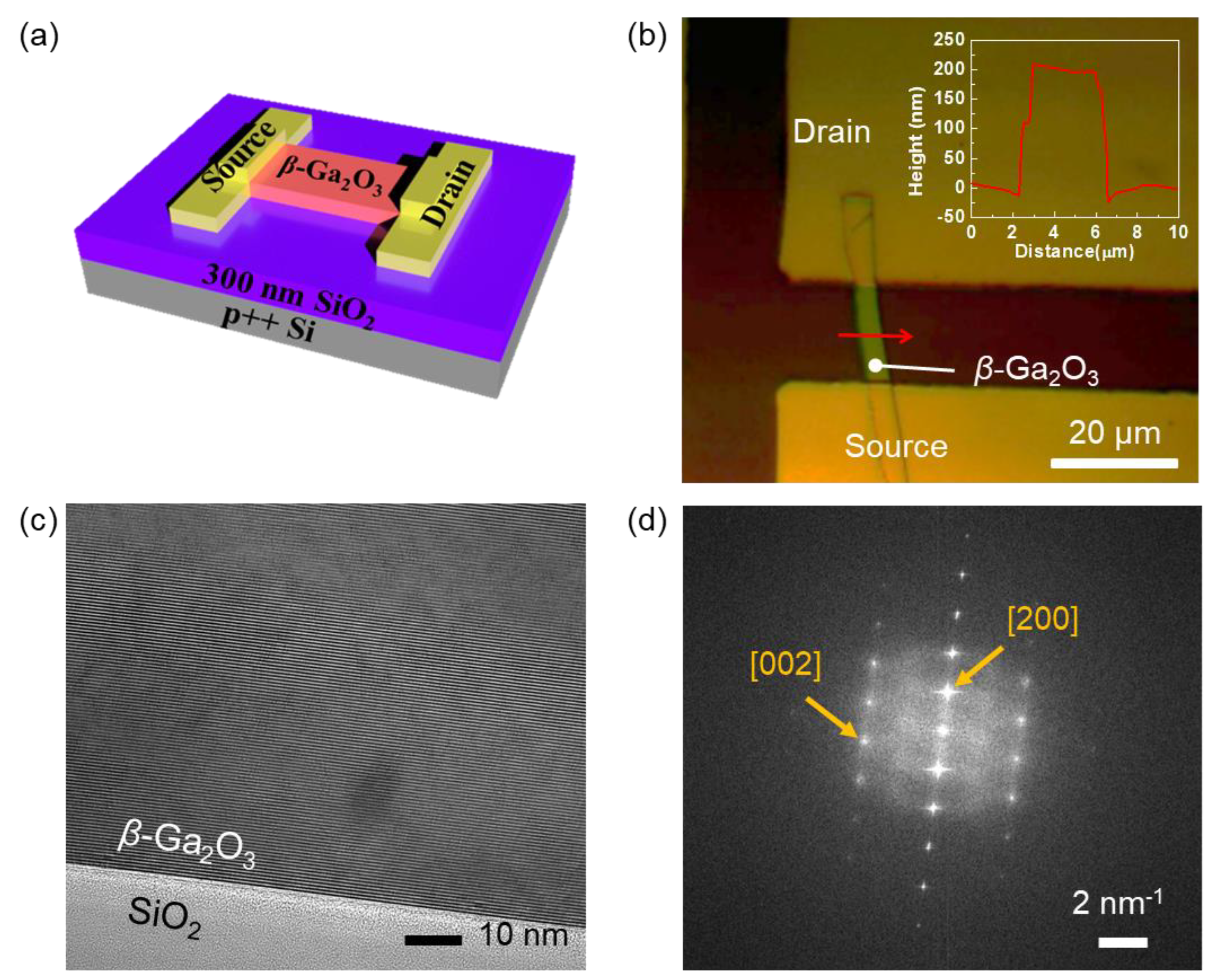
2.1. Device Fabrication

The (−201) surface β-Ga2O3 bulk substrate with unintentional n-type doping was purchased from Tamura Corporation, Japan. Multi-layer β-Ga2O3 flakes were mechanically transferred using a conventional scotch tape method from the β-Ga2O3 bulk substrate onto a heavily doped p-type Si substrate with thermally grown 300 nm SiO2. The source and drain electrodes were defined on top of the Ga2O3 flakes by photolithography, 20/100 nm Ti/Au electron-beam evaporation, and a conventional lift-off process. The fabricated device was annealed at 450 °C in nitrogen ambient for 1 min using a rapid thermal process to improve contact resistance.

2.2. Temperature-Dependent Electrical Measurements

The fabricated device was mounted in a liquid helium closed-cycle cryostat (Janis Research, CCS-150, Woburn, MA, USA). Temperature-dependent electrical characteristic measurements were carried out in a high vacuum (<10−3 Pa) with a semiconductor parameter analyzer (Keithley, 4200A-SCS, Solon, OH, USA) to identify the intrinsic effects without ambient environmental effects like water and oxygen molecules. To obtain the transfer curves, the gate bias (VGS) was swept from −40 to 10 V (forward sweep) and then back to −40 V (backward sweep) while maintaining drain bias (VDS) values of 0.5 and 1 V. The output characteristics were measured by sweeping VDS from 0 to 10 V while varying the VGS (−15, −10, −5, 0, 5, and 10 V). The transient response was measured by the alternate VGS at a fixed VDS of 1 V. To reach equilibrium, we first applied VGS of 10 V for 600 s until IDS was saturated. Gate pulses were then changed from 10 V to 0 V and maintained for 150 s, and vice versa.

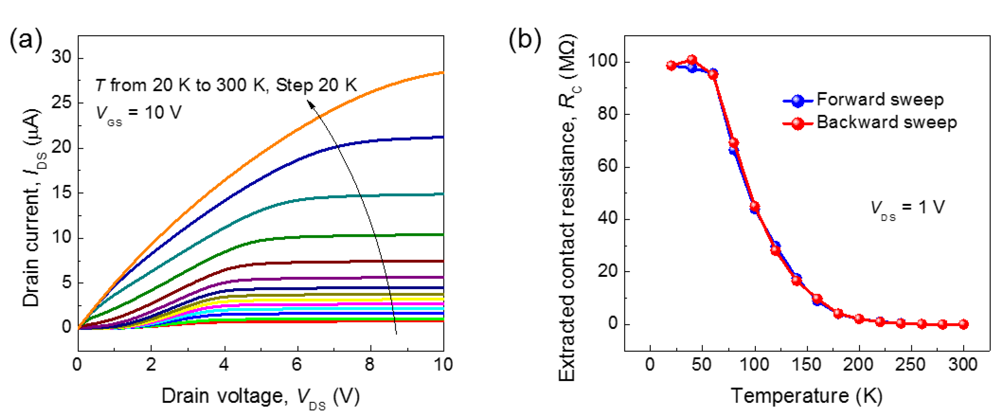
2.3. Contact Resistance, Mobility, and Threshold Voltage Extraction

The contact resistance (RC) was calculated as follows: RC = L·θ/(W·COX·μ0), where θ is the effective mobility attenuation factor, W is the channel width, L is the channel length, COX is the capacitance of the SiO2, and μ0 is the low-field mobility [29]. The low-field mobility was extracted from the Y-function, given by Y = (μ0·COX·VDS·W/L)0.5(VGSVth,Y), where Vth,Y was the threshold voltage extracted from Y-function. The effective mobility attenuation factor was extracted as follows:
I DS = ( μ 0 1   +   θ ( V G S     V t h , Y )   ) C ox W L ( V G S     V t h , Y ) V D S
We extracted the contact resistance and the mobility from the same transfer curve measured at VDS = 1 V. The mobility was extracted from the transfer characteristics. To observe the mobility except for the effect of contact resistance, we first extracted the actually applied drain voltage in the channel (VDS,CH) as follows: VDS,CH = VDSRC × IDS. Subsequently, the field-effect mobility was calculated as μFE = L·gm/(W·COX·VDS,CH), where gm is the transconductance. We estimated the threshold voltage as the x-intercept of the tangential line at the maximum slope on the transfer curve on a linear scale (Figure S1 in Supplementary Materials).

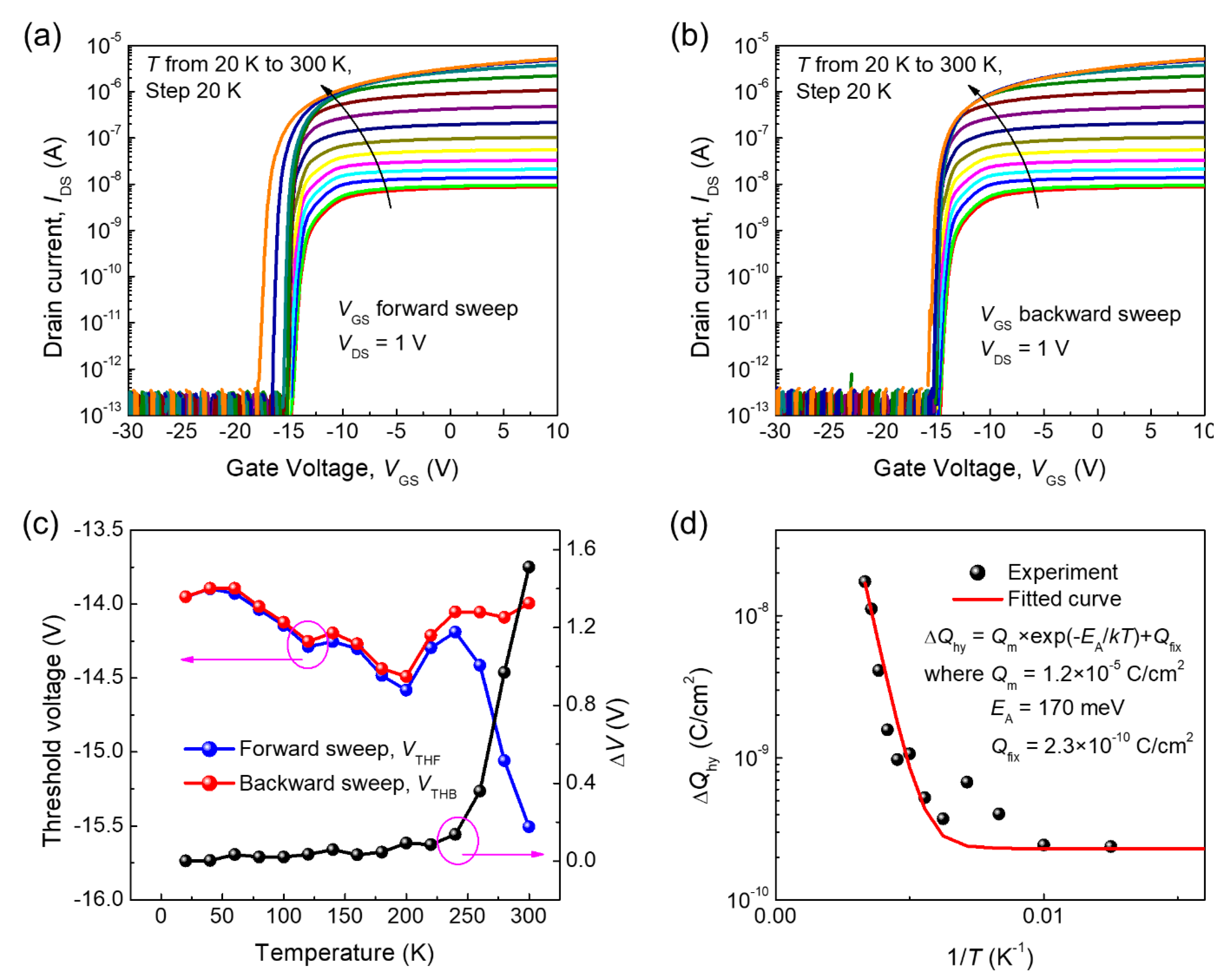
2.4. The Interface Trap Density, the Amount of Charge, Time-Dependent Trapped Charge Density Changes, and Trap Parameter Extraction

The interface trap density is estimated from SS = ln(10)·kT/q·(1+(CS+Cit)/COX), where SS is the subthreshold swing, CS is the capacitance of β-Ga2O3 conducting channel and Cit = q2 × Dit is the capacitance induced by the interface trap density [4,30]. The amount of charge trapped and de-trapped by the interface trap is extracted as ΔQhy = COX × ΔV. To determine the activation energy of the interface trap, ΔQhy was fitted by ΔQhy = Qm × exp(−EA/kBT) + Qfix, where Qm is the maximum charge density, kB is the Boltzmann constant, and Qfix is the temperature-independent fixed charge density [30].
The time-dependent density of the trapped charges changes is expressed as Qit(t) – Qit(0) = – (IDS(t) – IDS(0))ε·ε0/q·tOX·gm, where Qit(t) is the density of trapped charges (Qit) as a function of time, Qit(0) is Qit at the time changed the gate pulses, IDS(t) is IDS as a function of time, IDS(0) is IDS at the edge of gate pulses, ε is the relative dielectric constant of the oxide, ε0 is the permittivity of vacuum, and tOX is the thickness of the oxide. The transient Qit(t) – Qit(0) is fitted with a bi-exponential equation: Qit(t) – Qit(0) = Q1·exp(–t/τit1) + Q2·exp(–t/τit2), where Q1 and Q2 are the density of trapped charges and τit1 and τit2 are the time constants [26].

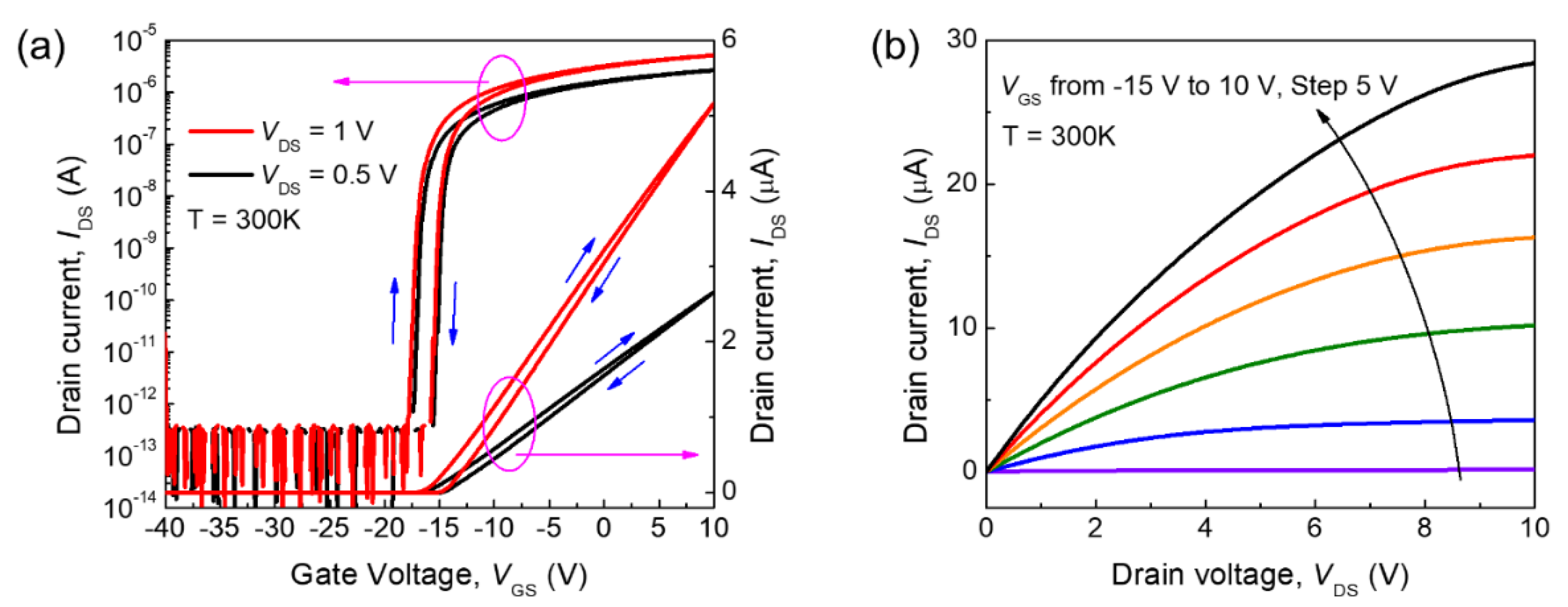
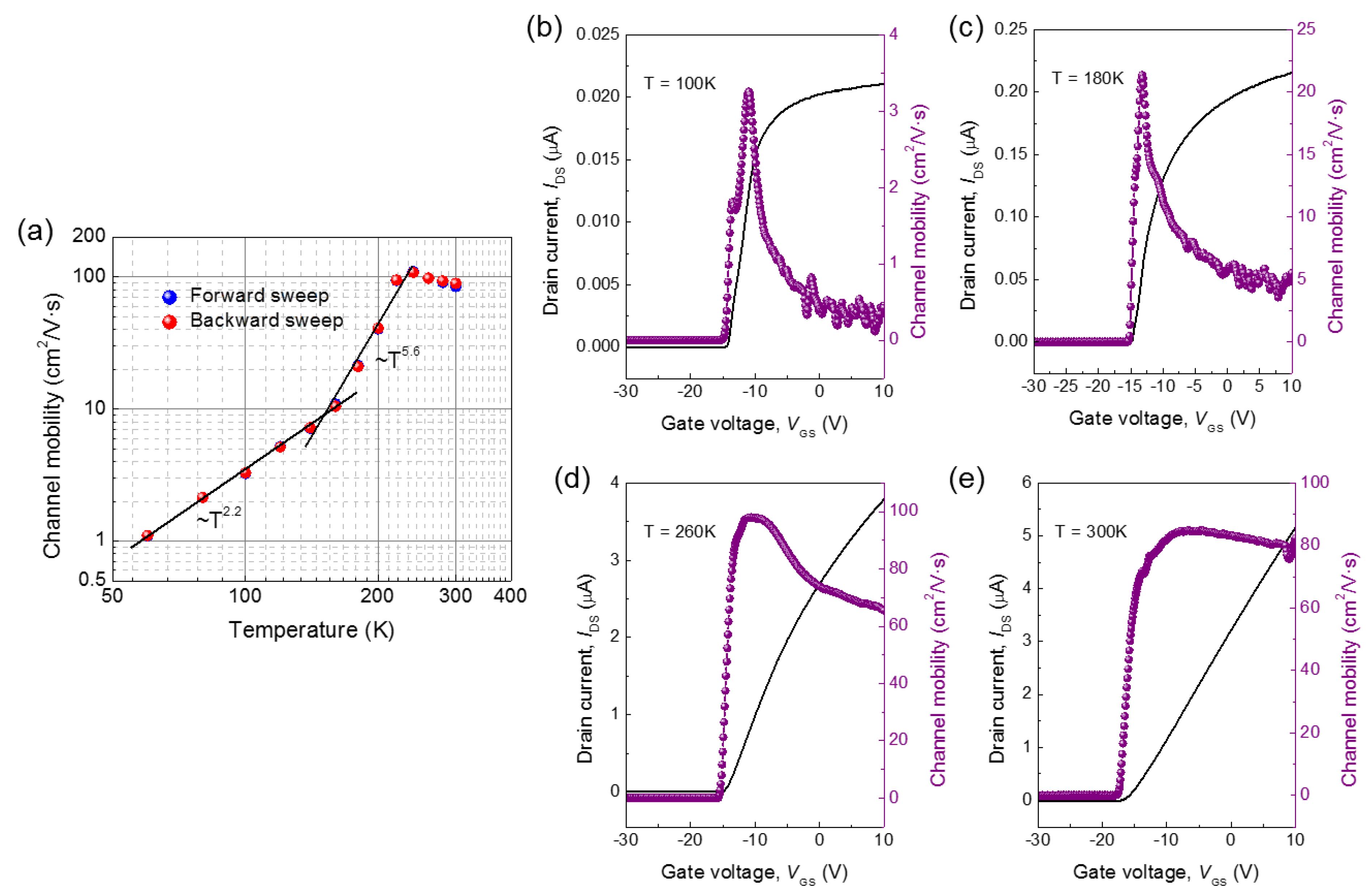
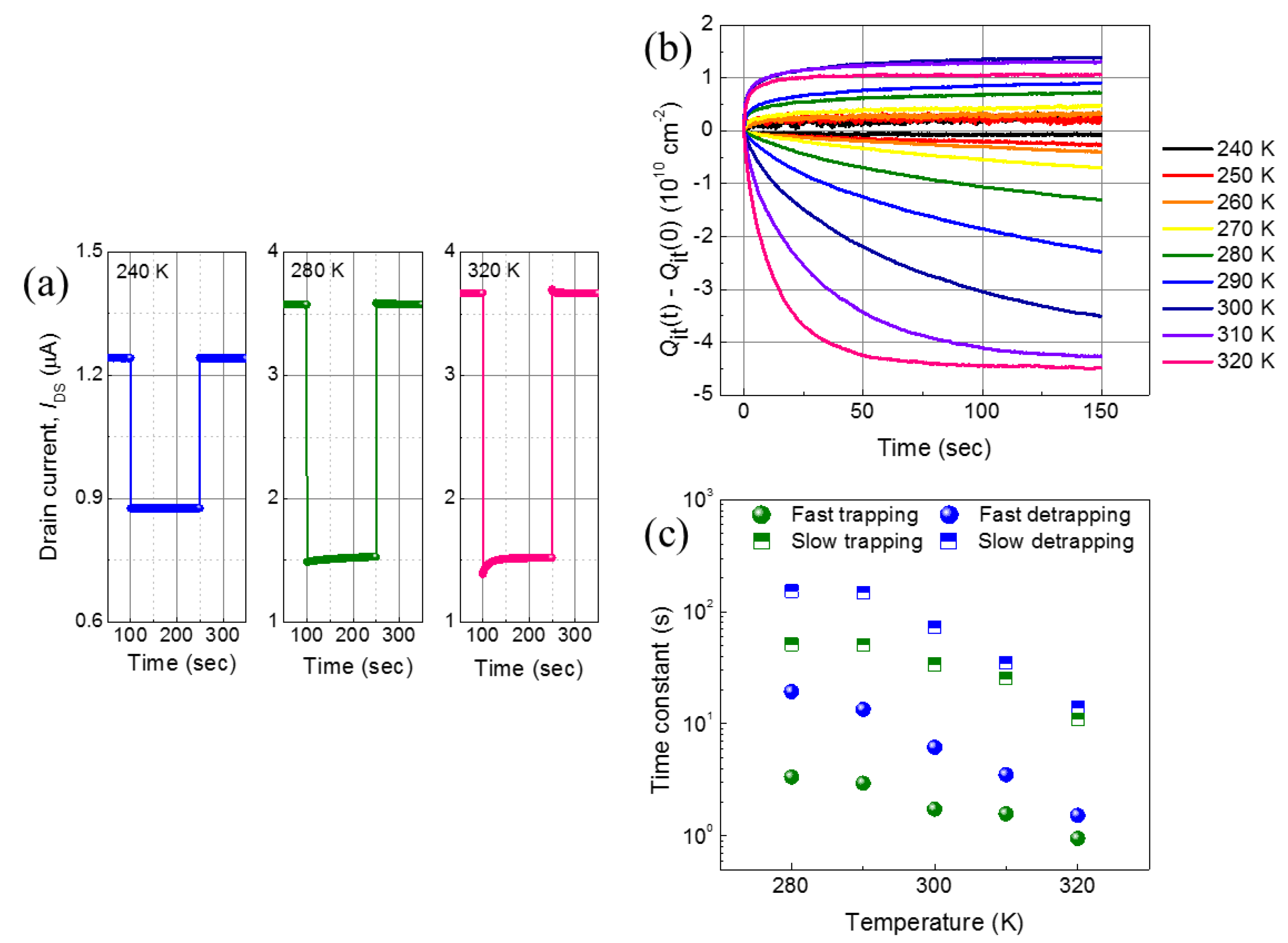
3. Results and Discussion

The schematic in Figure 1a shows the fabricated β-Ga2O3 FET on a heavily doped p-type Si substrate as the bottom gate with SiO2 gate insulator. SiO2 is potentially of a higher dielectric reliability in FETs due to the larger conduction band offset between SiO2 and Ga2O3 compared to Al2O3 and Ga2O3 [28]. Figure 1b shows an optical microscope image of the fabricated β-Ga2O3 device, and we measured W as 3.3 μm and L as 15 μm. A thickness of the β-Ga2O3 channel layer was measured as approximately 200 nm using atomic force microscopy (the inset in Figure 1b). A cross-sectional high resolution transmission electron microscopy (HR-TEM) image in Figure 1c represents the smooth interface between β-Ga2O3 and SiO2. Mechanical exfoliation of β-Ga2O3 and subsequent transfer on SiO2 did not result in any damage or defect, and a high quality of crystalline was preserved in the fabricated device. The selective-area diffraction pattern was also characterized as shown in Figure 1d. [200] and [002] directions in monoclinic crystal structure were indicated, and the channel surface was confirmed as the β-Ga2O3(100) plane.
The fabricated β-Ga2O3 FET was characterized by measuring its current-voltage characteristics. Figure 2a,b presents the measured transfer and output characteristics at room temperature, respectively. The fabricated device operates in depletion mode. We extracted the mobility, subthreshold swing, and threshold voltage of the device at room temperature from the transfer characteristics. At VDS = 1 V, maximum μFE of the β-Ga2O3 FET were 83.5 and 88.3 cm2/V·s, SS were 180 and 130 mV/dec, and threshold voltages (Vth) were −15.5 and −14 V for forward and backward sweeps, respectively, and an ON/OFF ratio (ION/IOFF) of approximately 107 was observed. Hysteresis (~1.5 V), a threshold voltage difference in the transfer curves depending on the sweep directions, was observed. The Dit was estimated to be approximately 1.44 × 1011 cm–2eV–1 from SS at 300 K. The Dit extracted in this work is similar to the previously other reports [27,28]. We also confirmed Ohmic contact behaviors from good linearity of the output curves near 0 V (Figure S2 in Supplementary Materials).
The temperature-dependent hysteretic behaviors of two-dimensional materials were previously reported by our group [30], and in general, it is prevalent that the interface traps and associated charges are responsible for it. Therefore, to investigate the origin of the hysteresis in the β-Ga2O3 FET in detail, its temperature dependence was characterized. Figure 3a,b presents the respective transfer curves for forward and backward sweeps at various temperatures from 20–300 K, and two properties were observed from the temperature-dependent transfer curves. First, the drain on-current (above the threshold) decreased by approximately three orders of magnitude as the temperature varied from 300 to 20 K. Decreasing the temperature would have contributed to the mobility decrease, and a detailed discussion on this follows later on. Second, as the temperature increased, the threshold voltage in the forward sweep shifted more toward a negative value than the one in the backward sweep. In other words, the hysteresis increased as the temperature increased.
To analyze the hysteresis, we extracted the threshold voltage from the temperature-dependent transfer curves. Figure 3c shows the variations of the Vth (left) in the forward (VTHF, blue) and backward (VTHB, red) sweeps. For consistency, we applied the same method to extract the threshold voltages for different temperatures. Thus, despite the monotonic left-shift of the transfer curves as the temperature increased, the additional change of slope on a linear scale made the variations of the extracted threshold voltage look more or less random and uncorrelated with temperature. Since the degree of hysteresis (ΔV) is defined as the difference between VTHF and VTHB, any artifact made while obtaining an individual threshold voltage would be canceled out. As shown in Figure 3c, the variations in ΔV below 230 K were almost negligible but started to increase at around 230 K and rose sharply above 230 K due to the thermal activation of the interface traps and the associated charges responsible for the hysteresis. For a more quantitative analysis, the ΔQhy trapped and de-trapped by the interface trap was extracted and then fitted by an Arrhenius plot, as shown in Figure 3d. The best fit of ΔQhy was obtained with the fitting parameter values of Qm = 1.2×10⁻⁵ C/cm2, EA = 170 meV, and Qfix = 2.3×10⁻¹⁰ C/cm2 (see the Methods section for more detail). The interface trap is partially active at room temperature even if the activation energy of 170 meV is six to seven times greater than the thermal energy at room temperature. Qfix, the charge density irrespective of the temperature, is five orders of magnitude smaller than Qm. In other words, most of the interface trap charges responsible for the hysteresis are governed by the temperature. In addition to the temperature-dependent hysteresis, the drain current (IDS) decreased in the transfer curve because the mobility is reduced with decreasing temperature, and this temperature-dependent current drop was also observed in the output characteristics. As shown in Figure 4a, the saturation IDS decreased and the slope in the linear region decreased with decreasing temperature, due to an increase in contact resistance (RC) and a decrease in mobility. As can be seen, the IDS no longer showed linear dependence on the bias near the low VDS as the temperature decreased, and the RC values were no longer negligible at low temperature. We extracted the RC from the modified Ghibaudo Y-function method [29] and the mobility by considering the finite RC (see the Methods section for more details). The temperature-dependent RC was calculated for forward and backward sweeps of the transfer curve, as shown in Figure 4b. RC was 6.3 kΩ at 300 K and then rapidly increased up to 100.8 MΩ as the temperature decreased, possibly because of the reduced thermal energies of carriers for thermionic emission over the Schottky barrier.
The maximum channel mobilities (μCH) at various temperatures considering the effect of the contact resistance are plotted on a log-log scale in Figure 5a. It is worth noting that the channel mobility steeply decreased as the temperature decreased below 230 K. At low temperature (generally below 100 K), the mobility reduced due to the impurity scattering and became proportional to Tγ (γ = 1.5) as the reported Hall mobility [23,25,31,32] but here it decreased more quickly with γ at approximately 2.2 (T = ~150 K) and 5.6 (T = 150–230 K). Thus we cannot explain this mobility degradation by the impurity scattering, and the surface related scattering would be responsible for it. In Figure 5b–e, the transfer curves at T = 100, 180, 260, and 300 K are plotted on a linear scale, respectively, and the extracted channel mobilities in each are also shown alongside. Implausibly, IDS at 100 K rapidly saturated at just above the threshold whereas that at 300 K increased linearly. That is to say, the channel mobility became less affected by the gate bias as the temperature increased. Interestingly, the channel mobility started to decrease below 230 K (the temperature that coincides with the hysteresis becoming invisible). Therefore, these trends contributed to the interplay between interface scattering and the effect of acceptor-like traps at the interface between β-Ga2O3 and SiO2 [27]. At temperatures below 230 K, the acceptor-like traps were frozen and electrically neutral, allowing more electrons to drift along the vicinity of the interface. The interface scattering became predominant over any other scatterings including ionized impurity scattering, and mobility steeply decreased. This can also be envisioned by the strong gate bias dependence of the channel mobility at low temperature, as discussed earlier (Figure 5b), and the previous reports of strong mobility degradation by the surface effects in β-Ga2O3 thin-films at low temperatures [33].
We also carried out a time-domain analysis on the capture and release of charges by the traps at the interface by measuring the transient response to observe the behaviors of the traps [34]. As shown in Figure 6a, as soon as VGS dropped, IDS sharply dropped and then slowly increased because the captured carriers were released from the interface traps. At the rising edge of VGS, IDS popped up and then slowly decreased while maintaining VGS because of the electrons captured by the acceptor-like traps at the interface. As the temperature increased, these phenomena noticeably appeared because more of the acceptor-like traps were activated. We calculated the transient changes of the trapped charge density for the temperature from 240 to 320 K, as shown in Figure 6b; as the temperature increased, the changes of trapped and de-trapped charge density also increased. The transient changes were not observed below 240 K because of negligible variation by the trapped charge. Figure 6c shows temperature-dependent time constants extracted by fitting Figure 6b with a bi-exponential equation [35]. All of the time constants for the slow and fast processes decreased as the temperature increased because the activated traps were more abundant and the electrons were more thermally energized. We also observed that the charge trapping processes were faster than the charge de-trapping processes. The detailed time constants are available in the Supplementary Materials (Table S1).

4. Conclusions

In summary, we investigated the effect of interface traps on the degradation of channel mobility and hysteresis in a bottom-gated β-Ga2O3 FET at low temperature. Temperature-dependent electrical characterizations were performed on the device in the temperature range of 20–300 K, and variations in threshold voltage and field-effect mobility and the degree of hysteresis were analyzed. The activation energy of the interface trap between β-Ga2O3 and SiO2 was estimated as 170 meV, and there was no observable hysteresis below 230 K. As the acceptor-like traps at the interface are frozen and inactive at low temperature, the hysteresis disappears and it was simultaneously found that the channel mobility sharply decreases. This was understood as the frozen charged traps allow the channel electrons to collide at the interface, which was also confirmed by the vulnerability of mobility to gate bias at low temperature. Furthermore, the charge trapping and de-trapping processes at the interface were studied in the time-domain by switching the gate bias. At higher temperatures, the extracted time constants for the slow and fast processes became shorter due to more activated traps. We believe that understanding the role of the interface traps between the gate insulator and β-Ga2O3 could help to optimize the fabrication and operation of β-Ga2O3-based devices in a variety of circumstances, particularly in harsh environments in space and military applications.

Supplementary Materials

The following are available online at https://www.mdpi.com/2079-4991/11/2/494/s1, Figure S1. Transfer curve for VDS = 1 V in a linear scale at 180 K, Figure S2. Output curves of IDS-low VDS at room temperature, Table S1. The density of the trapped and de-trapped charges and the time constants.

Author Contributions

Conceptualization: G.Y. and J.H.; methodology: Y.P. and J.M.; formal analysis: Y.P.; investigation: Y.P.; writing—original draft preparation: Y.P. and J.M.; writing—review and editing: G.Y. and J.H.; visualization: Y.P. and J.M.; supervision: G.Y. and J.H.; project administration: J.H.; funding acquisition: J.H. All authors have read and agreed to the published version of the manuscript.

Funding

This study was supported by the Industrial Strategic Technology Development Program (20000300) funded by the Ministry of Trade, Industry, and Energy (MOTIE, Republic of Korea), and Human Resources Program in Energy Technology of the Korea Institute of Energy Technology Evaluation and Planning, granted financial resource from the MOTIE, Republic of Korea (no. 20184030202220).

Data Availability Statement

The data presented in this study are available on request from thecorresponding author.

Conflicts of Interest

The authors declare no conflict of interest. The funders had no role in the design of the study; in the collection, analyses, or interpretation of data; in the writing of the manuscript; or in the decision to publish the results.

References

  1. Kim, M.; Seo, J.-H.; Singisetti, U.; Ma, Z. Recent advances in free-standing single crystalline wide band-gap semiconductors and their applications: GaN, SiC, ZnO, β-Ga2O3, and diamond. J. Mater. Chem. C 2017, 5, 8338–8354. [Google Scholar] [CrossRef]
  2. Bhuiyan, M.A.; Zhou, H.; Jiang, R.; Zhang, E.X.; Fleetwood, D.M.; Ye, P.D.; Ma, T. Charge Trapping in Al2O3/β-Ga2O3-Based MOS Capacitors. IEEE Electron Device Lett. 2018, 39, 1022–1025. [Google Scholar] [CrossRef]
  3. Nagarajan, L.; De Souza, R.A.; Samuelis, D.; Valov, I.; Börger, A.; Janek, J.; Becker, K.-D.; Schmidt, P.C.; Martin, M. A chemically driven insulator–metal transition in non-stoichiometric and amorphous gallium oxide. Nat. Mater. 2008, 7, 391–398. [Google Scholar] [CrossRef] [Green Version]
  4. Zhou, H.; Maize, K.; Noh, J.; Shakouri, A.; Ye, P.D. Thermodynamic Studies of β-Ga2O3 Nanomembrane Field-Effect Transistors on a Sapphire Substrate. ACS Omega 2017, 2, 7723–7729. [Google Scholar] [CrossRef] [PubMed] [Green Version]
  5. Ma, J.; Lee, O.; Yoo, G. Effect of Al2O3 Passivation on Electrical Properties of β-Ga2O3 Field-Effect Transistor. IEEE J. Electron Devices Soc. 2019, 7, 512–516. [Google Scholar] [CrossRef]
  6. Pozina, G.; Forsberg, M.; Kaliteevski, M.A.; Hemmingsson, C. Emission properties of Ga2O3 nano-flakes: Effect of excitation density. Sci. Rep. 2017, 7, 42132. [Google Scholar] [CrossRef] [Green Version]
  7. Ma, J.; Lee, O.; Yoo, G. Abnormal Bias-Temperature Stress and Thermal Instability of β-Ga2O3 Nanomembrane Field-Effect Transistor. IEEE J. Electron Devices Soc. 2018, 6, 1124–1128. [Google Scholar] [CrossRef]
  8. Polyakov, A.Y.; Smirnov, N.B.; Shchemerov, I.V.; Chernykh, S.V.; Oh, S.; Pearton, S.J.; Ren, F.; Kochkova, A.; Kim, J. Defect States Determining Dynamic Trapping-Detrapping in β-Ga2O3 Field-Effect Transistors. ECS J. Solid State Sci. Technol. 2019, 8, Q3013–Q3018. [Google Scholar] [CrossRef]
  9. Higashiwaki, M.; Sasaki, K.; Murakami, H.; Kumagai, Y.; Koukitu, A.; Kuramata, A.; Masui, T.; Yamakoshi, S. Recent progress in Ga2O3 power devices. Semicond. Sci. Technol. 2016, 31, 34001. [Google Scholar] [CrossRef]
  10. Higashiwaki, M.; Sasaki, K.; Kuramata, A.; Masui, T.; Yamakoshi, S. Gallium oxide (Ga2O3) metal-semiconductor field-effect transistors on single-crystal β-Ga2O3 (010) substrates. Appl. Phys. Lett. 2012, 100, 13504. [Google Scholar] [CrossRef]
  11. Sasaki, K.; Higashiwaki, M.; Kuramata, A.; Masui, T.; Yamakoshi, S. Si-Ion Implantation Doping in β-Ga2O3and Its Application to Fabrication of Low-Resistance Ohmic Contacts. Appl. Phys. Express 2013, 6, 86502. [Google Scholar] [CrossRef]
  12. Tak, B.R.; Garg, M.; Kumar, A.; Gupta, V.; Singh, R. Gamma Irradiation Effect on Performance of β-Ga2O3 Metal-Semiconductor-Metal Solar-Blind Photodetectors for Space Applications. ECS J. Solid State Sci. Technol. 2019, 8, Q3149–Q3153. [Google Scholar] [CrossRef]
  13. Oh, S.; Kim, J.; Ren, F.; Pearton, S.J.; Kim, J. Quasi-two-dimensional β-gallium oxide solar-blind photodetectors with ultrahigh responsivity. J. Mater. Chem. C 2016, 4, 9245–9250. [Google Scholar] [CrossRef]
  14. Guo, D.; An, Y.; Cui, W.; Zhi, Y.; Zhao, X.; Lei, M.; Li, L.; Li, P.; Wu, Z.; Tang, W. Epitaxial growth and magnetic properties of ultraviolet transparent Ga2O3/(Ga1−xFex)2O3 multilayer thin films. Sci. Rep. 2016, 6, 25166. [Google Scholar] [CrossRef] [PubMed] [Green Version]
  15. Zhou, H.; Alghmadi, S.; Si, M.; Qiu, G.; Ye, P.D. Al2O3/β-Ga2O3(-201) Interface Improvement Through Piranha Pretreatment and Postdeposition Annealing. IEEE Electron Device Lett. 2016, 37, 1411–1414. [Google Scholar] [CrossRef]
  16. Baliga, B.J. Power semiconductor device figure of merit for high-frequency applications. IEEE Electron Device Lett. 1989, 10, 455–457. [Google Scholar] [CrossRef]
  17. Wang, H.; Wang, F.; Zhang, J. Power Semiconductor Device Figure of Merit for High-Power-Density Converter Design Applications. IEEE Trans. Electron Devices 2008, 55, 466–470. [Google Scholar] [CrossRef]
  18. Swinnich, E.; Hasan, M.N.; Zeng, K.; Dove, Y.; Singisetti, U.; Mazumder, B.; Seo, J.-H. Flexible β-Ga2O3 Nanomembrane Schottky Barrier Diodes. Adv. Electron. Mater. 2019, 5, 1800714. [Google Scholar] [CrossRef]
  19. Kim, J.; Mastro, M.A.; Tadjer, M.J.; Kim, J. Quasi-Two-Dimensional h-BN/β-Ga2O3 Heterostructure Metal–Insulator–Semiconductor Field-Effect Transistor. ACS Appl. Mater. Interfaces 2017, 9, 21322–21327. [Google Scholar] [CrossRef]
  20. Hoefer, U.; Frank, J.; Fleischer, M. High temperature Ga2O3-gas sensors and SnO2-gas sensors: A comparison. Sens. Actuators B Chem. 2001, 78, 6–11. [Google Scholar] [CrossRef]
  21. Huang, J.R.; Hsu, W.C.; Chen, Y.J.; Wang, T.B.; Lin, K.W.; Chen, H.I.; Liu, W.C. Comparison of hydrogen sensing characteristics for Pd/GaN and Pd/Al0.3Ga0.7As Schottky diodes. Sens. Actuators B Chem. 2006, 117, 151–158. [Google Scholar] [CrossRef]
  22. You, A.; Be, M.A.Y.; In, I. High-performance metal-semiconductormetal deep-ultraviolet photodetectors based on homoepitaxial diamond thin film. Appl. Phys. Lett. 2006, 89, 113509. [Google Scholar]
  23. Moser, N.; McCandless, J.; Crespo, A.; Leedy, K.; Green, A.; Neal, A.; Mou, S.; Ahmadi, E.; Speck, J.; Chabak, K.; et al. Ge-Doped β-Ga2O3 MOSFETs. IEEE Electron Device Lett. 2017, 38, 775–778. [Google Scholar] [CrossRef]
  24. Züttel, A. Materials for hydrogen storage. Mater. Today 2003, 6, 24–33. [Google Scholar] [CrossRef]
  25. Zhang, Y.; Alema, F.; Mauze, A.; Koksaldi, O.S.; Miller, R.; Osinsky, A.; Speck, J.S. MOCVD grown epitaxial β-Ga2O3 thin film with an electron mobility of 176 cm2/V s at room temperature. APL Mater. 2018, 7, 22506. [Google Scholar] [CrossRef] [Green Version]
  26. Sbrockey, N.M.; Salagaj, T.; Coleman, E.; Tompa, G.S.; Moon, Y.; Kim, M.S. Large-Area MOCVD Growth of Ga2O3 in a Rotating Disc Reactor. J. Electron. Mater. 2015, 44, 1357–1360. [Google Scholar] [CrossRef]
  27. Bae, H.; Noh, J.; Alghamdi, S.; Si, M.; Ye, P.D. Ultraviolet Light-Based Current–Voltage Method for Simultaneous Extraction of Donor- and Acceptor-Like Interface Traps in β-Ga2O3 FETs. IEEE Electron Device Lett. 2018, 39, 1708–1711. [Google Scholar] [CrossRef]
  28. Jayawardena, A.; Ramamurthy, R.P.; Ahyi, A.C.; Morisette, D.; Dhar, S. Interface trapping in (2¯01) β-Ga2O3 MOS capacitors with deposited dielectrics. Appl. Phys. Lett. 2018, 112, 192108. [Google Scholar] [CrossRef]
  29. Chang, H.-Y.; Zhu, W.; Akinwande, D. On the mobility and contact resistance evaluation for transistors based on MoS2 or two-dimensional semiconducting atomic crystals. Appl. Phys. Lett. 2014, 104, 113504. [Google Scholar] [CrossRef]
  30. Park, Y.; Baac, H.W.; Heo, J.; Yoo, G. Thermally activated trap charges responsible for hysteresis in multilayer MoS2 field-effect transistors. Appl. Phys. Lett. 2016, 108, 83102. [Google Scholar] [CrossRef]
  31. Kabilova, Z.; Kurdak, C.; Peterson, R.L. Observation of impurity band conduction and variable range hopping in heavily doped (010) β-Ga2O3. Semicond. Sci. Technol. 2019, 34, 03LT02. [Google Scholar] [CrossRef]
  32. Irmscher, K.; Galazka, Z.; Pietsch, M.; Uecker, R.; Fornari, R. Electrical properties of β-Ga2O3 single crystals grown by the Czochralski method. J. Appl. Phys. 2011, 110, 63720. [Google Scholar] [CrossRef]
  33. Ahrling, R.; Boy, J.; Handwerg, M.; Chiatti, O.; Mitdank, R.; Wagner, G.; Galazka, Z.; Fischer, S.F. Transport Properties and Finite Size Effects in β-Ga2O3 Thin Films. Sci. Rep. 2019, 9, 13149. [Google Scholar] [CrossRef] [PubMed]
  34. Zhang, W.; Zhang, Y.; Mao, W.; Ma, X.; Zhang, J.; Hao, Y. Influence of the Interface Acceptor-Like Traps on the Transient Response of AlGaN/GaN HEMTs. IEEE Electron Device Lett. 2013, 34, 45–47. [Google Scholar] [CrossRef]
  35. Guo, Y.; Wei, X.; Shu, J.; Liu, B.; Yin, J.; Guan, C.; Han, Y.; Gao, S.; Chen, Q. Charge trapping at the MoS2-SiO2 interface and its effects on the characteristics of MoS2 metal-oxide-semiconductor field effect transistors. Appl. Phys. Lett. 2015, 106, 103109. [Google Scholar] [CrossRef]
Figure 1. (a) Schematic of the β-Ga2O3 field-effect transistor, (b) Optical microscopy image of the fabricated field-effect transistor. The β-Ga2O3 channel thickness along the red line was characterized by atomic force microscopy, and the profile is shown in the inset. (c) Cross-sectional HR-TEM image of the interface between β-Ga2O3 channel and SiO2 insulator. (d) Selective area electron diffraction pattern of the β-Ga2O3.
Nanomaterials 11 00494 g001
Figure 2. Characteristics of the fabricated β-Ga2O3 field-effect transistor: (a) transfer characteristics for VDS = 0.5 (black line) and 1 V (red line) at room temperature (VGS was swept from –40 to 10 V (forward sweep) and then back to –40 V (backward sweep)), and (b) output characteristics for VGS = –15, –10, –5, 0, and 5 V at room temperature of the fabricated β-Ga2O3 field-effect transistor.
Nanomaterials 11 00494 g002
Figure 3. Transfer characteristics of the fabricated β-Ga2O3 field-effect transistor: (a) forward sweep and (b) backward sweep at various temperatures from 20 to 300 K, (c) the temperature-dependent threshold voltage in the forward (blue) and backward (red) sweeps and the temperature-dependent degree of hysteresis (black; the difference between the threshold voltages in the forward and backward sweeps), and (d) Arrhenius plots of the ΔQhy trapped and de-trapped by the interface traps (the red solid line is the best fit of ΔQhy).
Nanomaterials 11 00494 g003
Figure 4. (a) Output characteristics at a gate bias (VGS) of 10 V in the temperature range of 20–300 K and (b) extracted contact resistance at VDS = 1 V of the fabricated β-Ga2O3 field-effect transistor in the forward (blue) and backward (red) sweeps.
Nanomaterials 11 00494 g004
Figure 5. (a) Maximum channel mobilities at various temperatures (T = 60–300 K) on a log-log scale (the black solid lines are the fitted channel mobilities proportional to approximately T2.2 (T = ~150 K) and T5.6 (T = 150–230 K)) and (be) transfer curves on a linear scale for T = 100, 180, 260, and 300 K with the extracted channel mobilities of the fabricated β-Ga2O3 field-effect transistor.
Nanomaterials 11 00494 g005
Figure 6. (a) Transient responses of IDS to the VGS changes at T = 240, 280, and 320 K, (b) changes of trapped charge density as a function of time from 240 to 320 K, and (c) the extracted temperature-dependent time constants for the slow and fast processes of the fabricated β-Ga2O3 field-effect transistor.
Nanomaterials 11 00494 g006
Publisher’s Note: MDPI stays neutral with regard to jurisdictional claims in published maps and institutional affiliations.

