
Three-Layer PdO/CuWO4/CuO System for Hydrogen Gas Sensing with Reduced Humidity Interference


Abstract
:1. Introduction
2. Materials and Methods
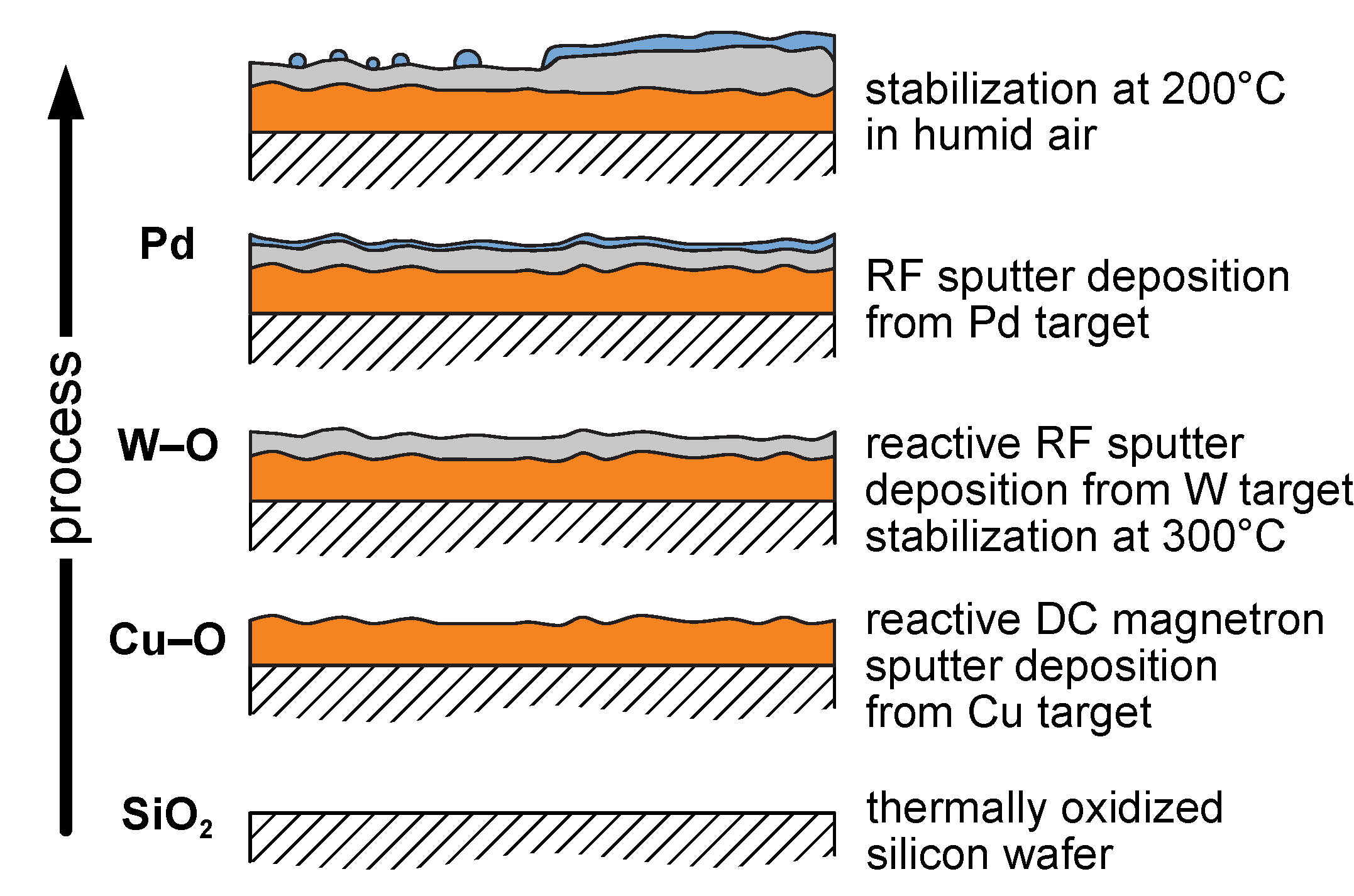
2.1. Material Synthesis
2.2. Material Analyses and Sensing Measurements
3. Results and Discussion
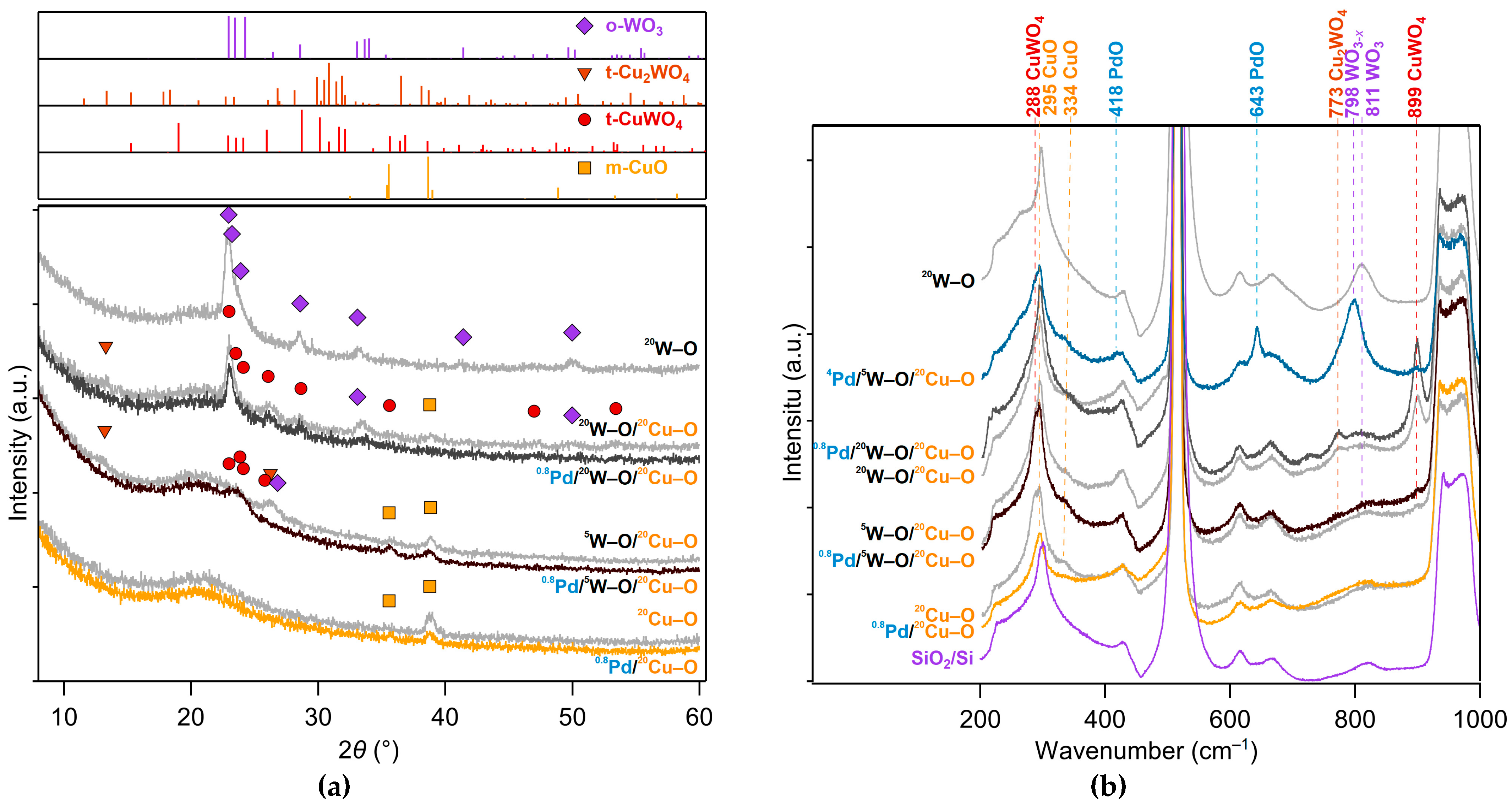
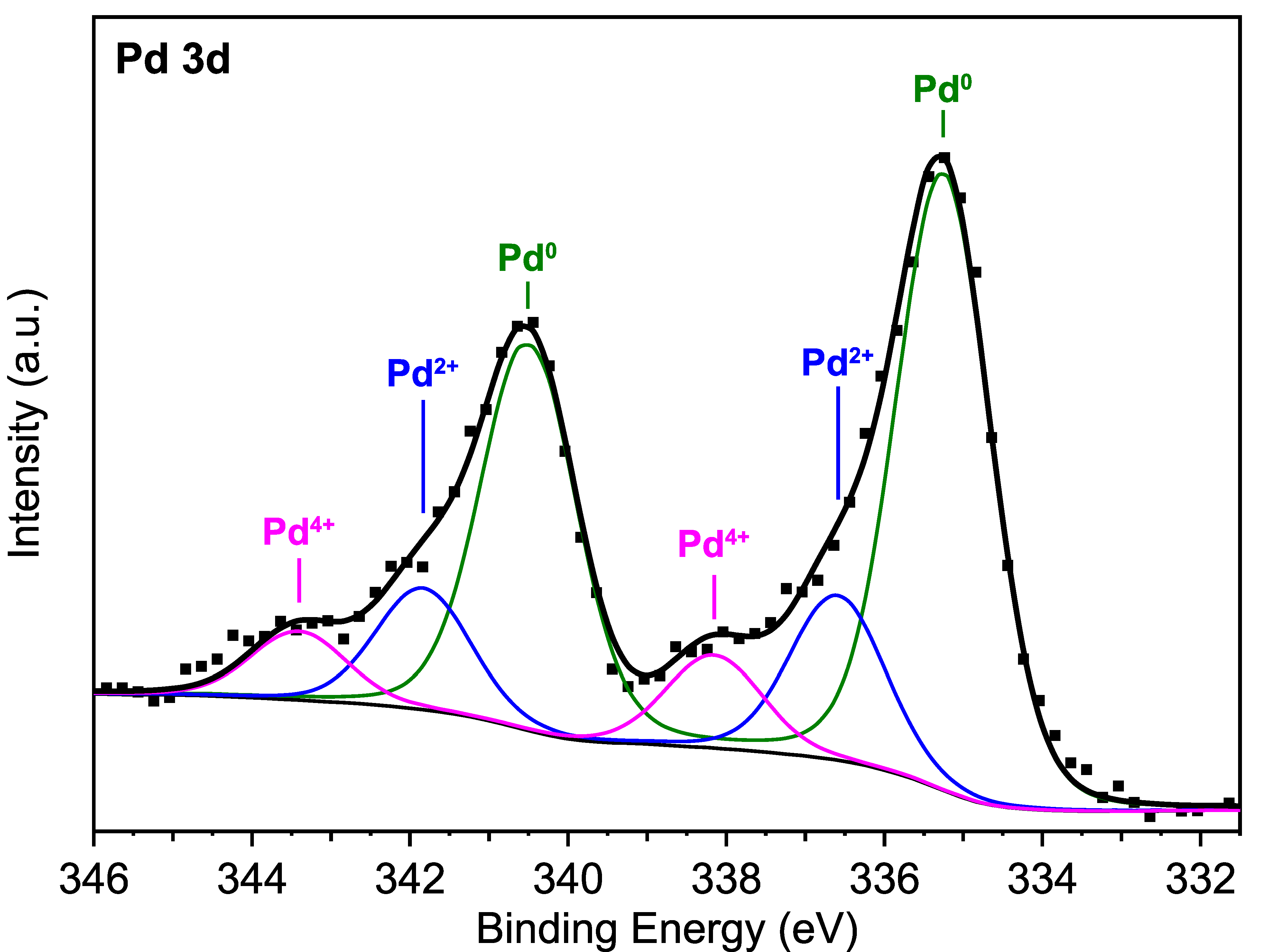
3.1. Structure
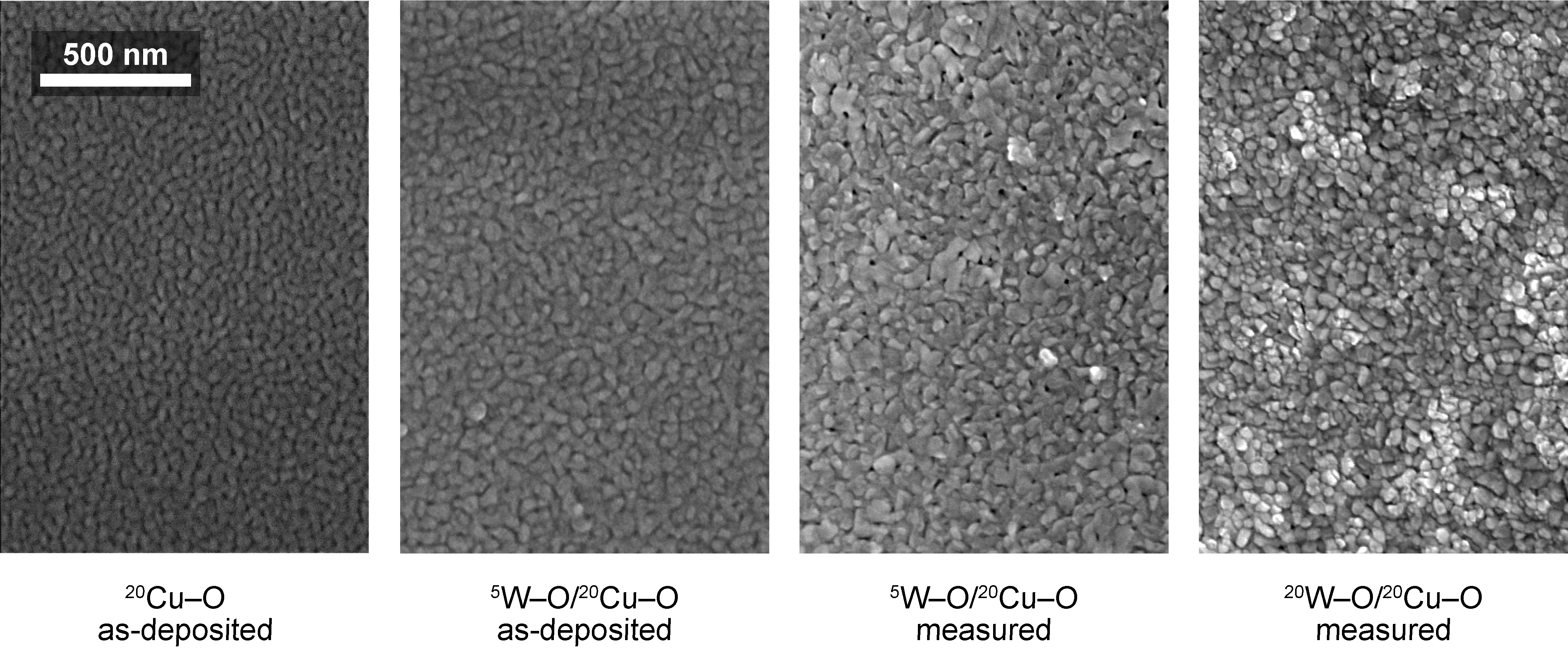
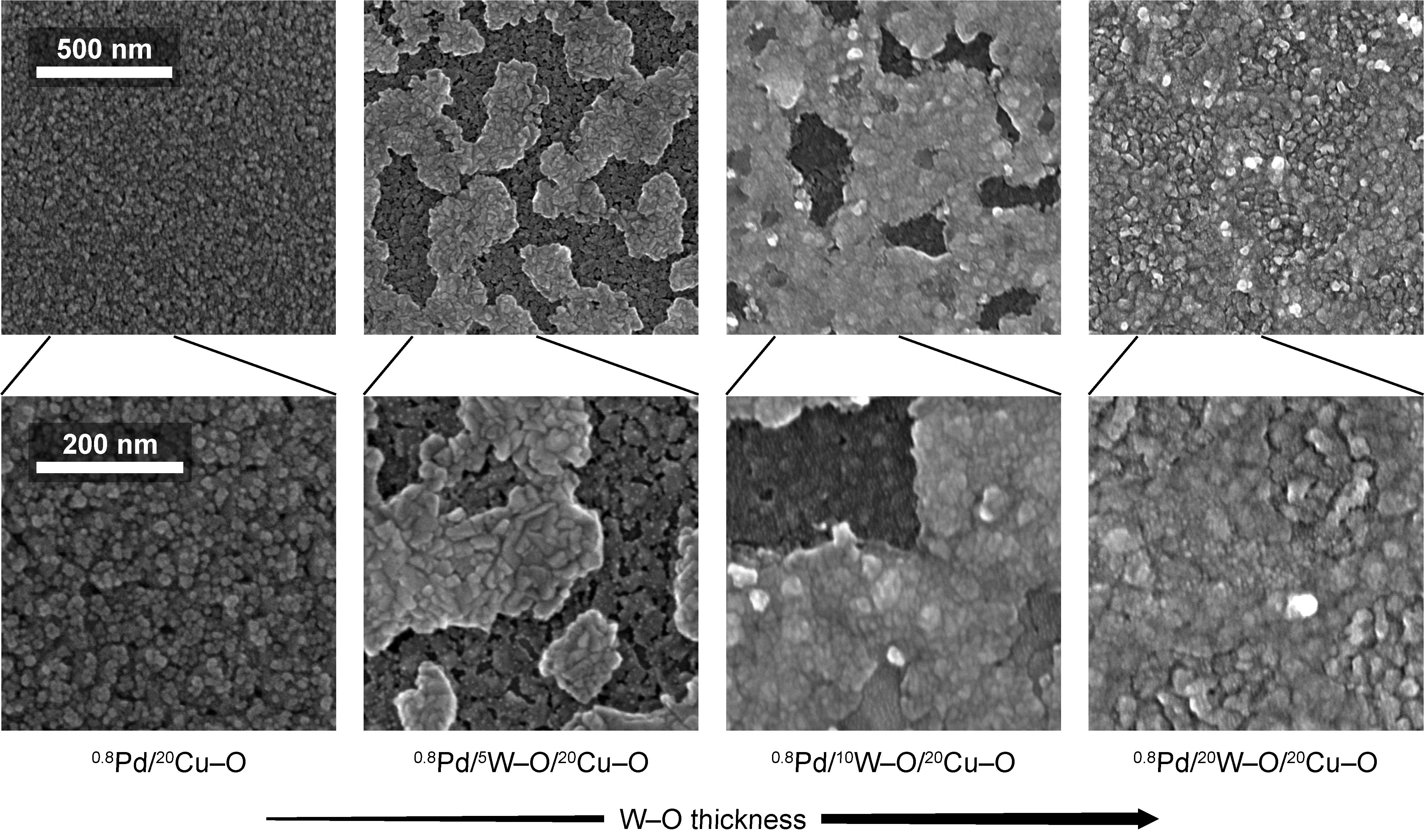
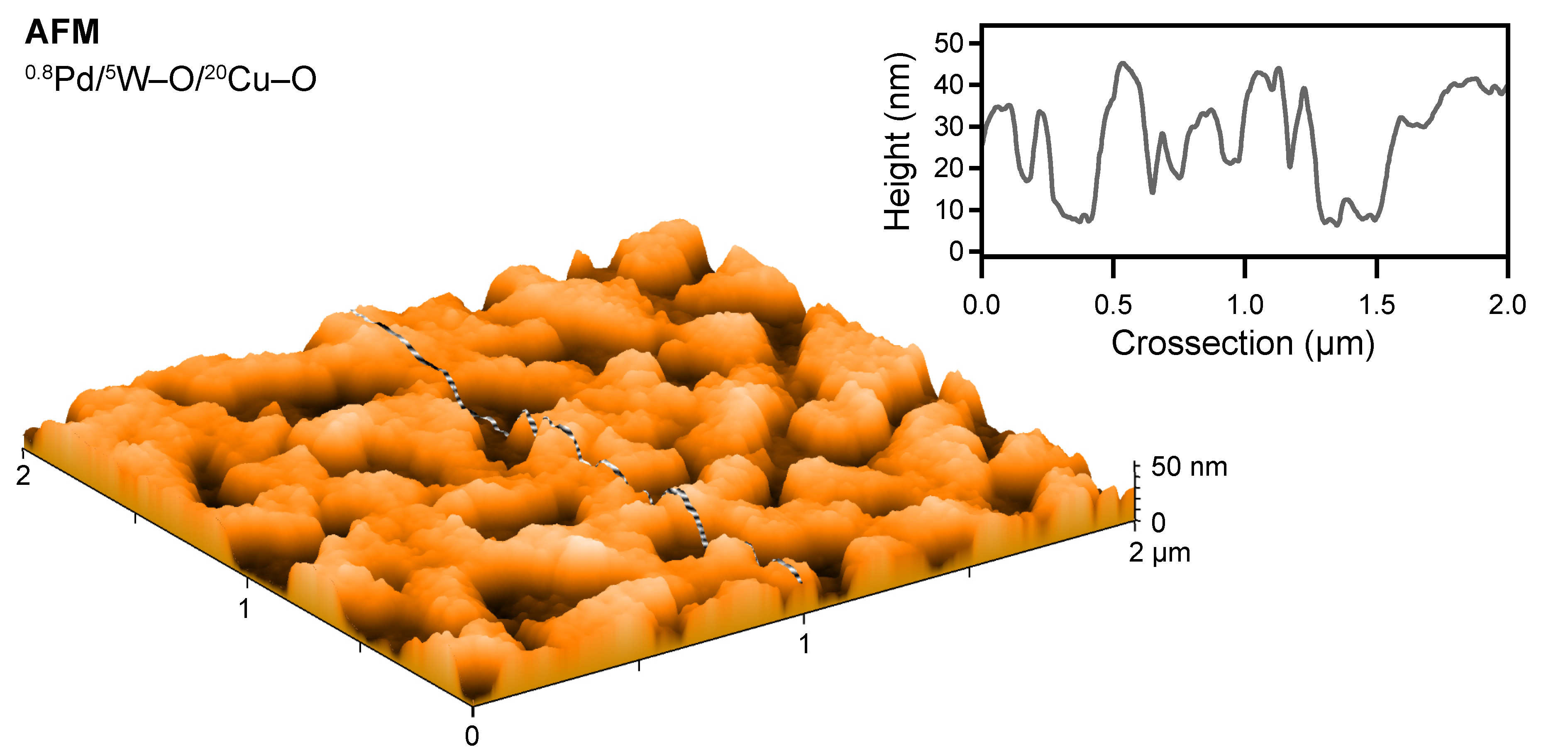
3.2. Surface Morphology
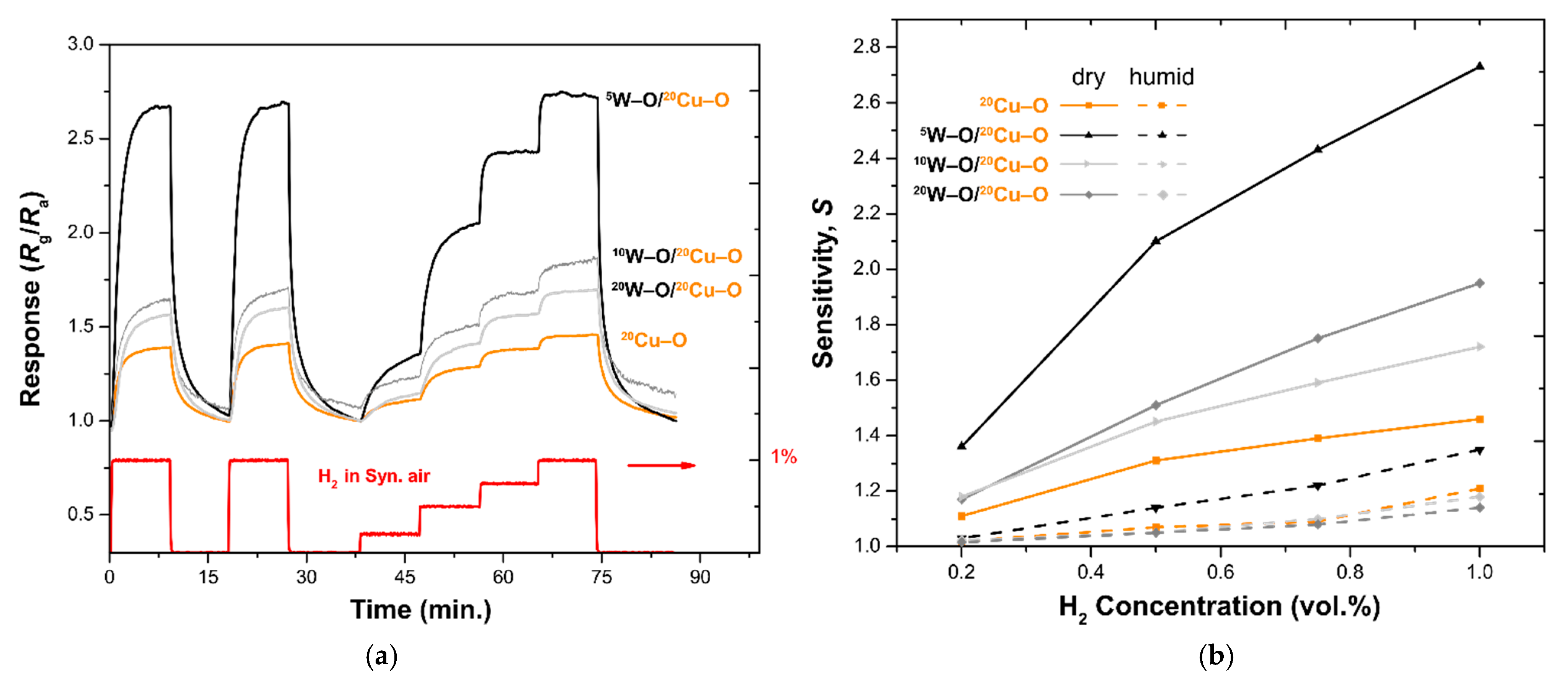
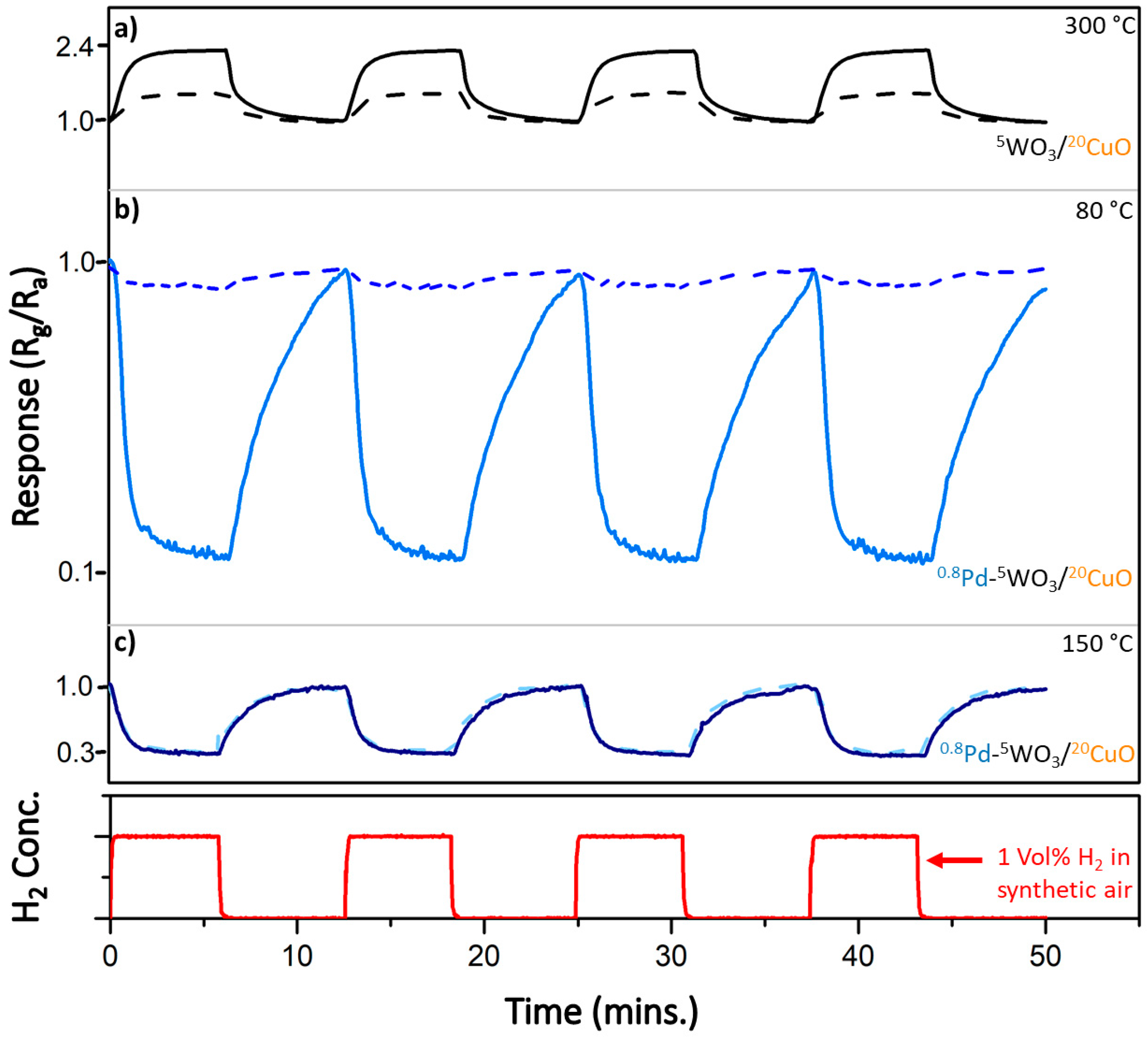
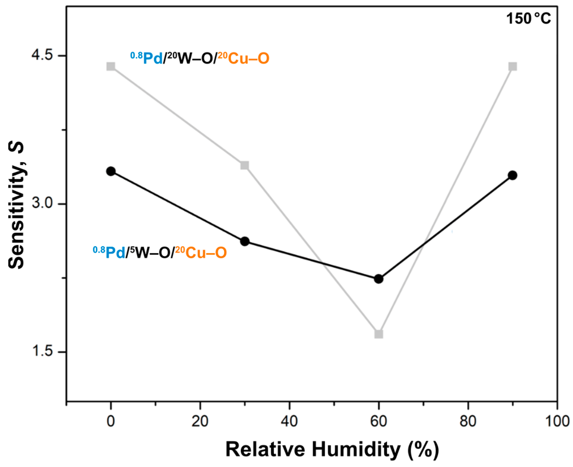
3.3. Sensing Response
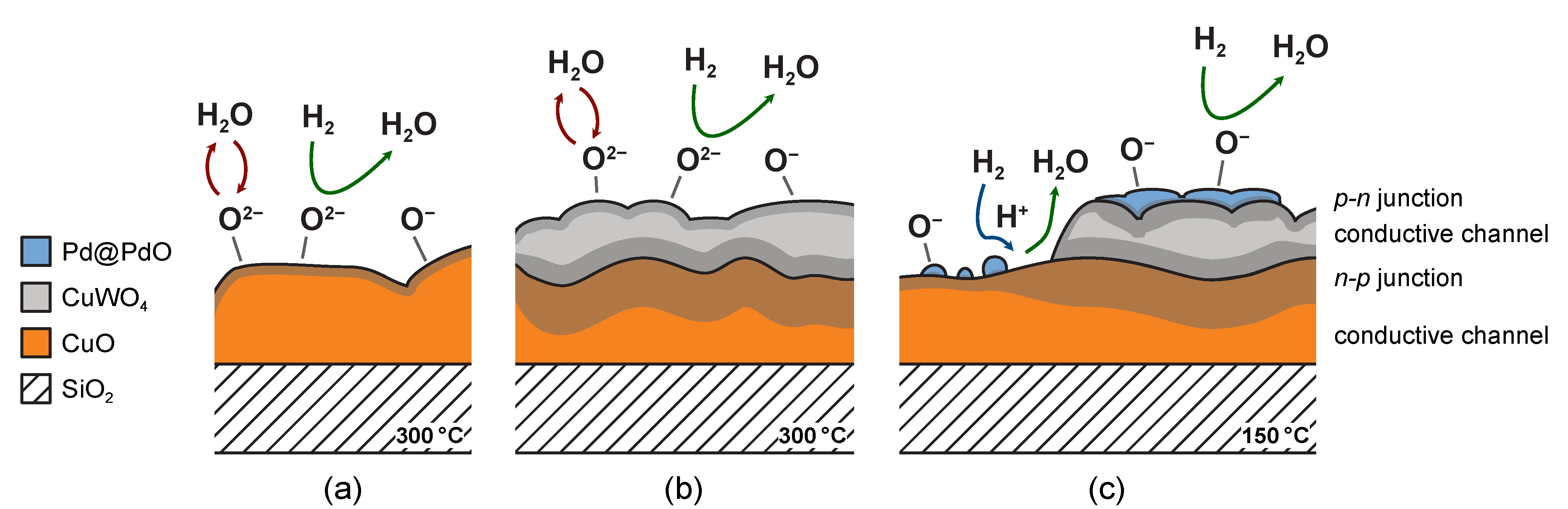
- (i)
- (ii)
- PdO favors the adsorption of oxygen over the hydroxyl groups [53].
- (iii)
- PdO forms another heterojunction (p–n) with the topmost layer of copper tungstate.
4. Conclusions
Supplementary Materials
Author Contributions
Funding
Data Availability Statement
Acknowledgments
Conflicts of Interest
Appendix A
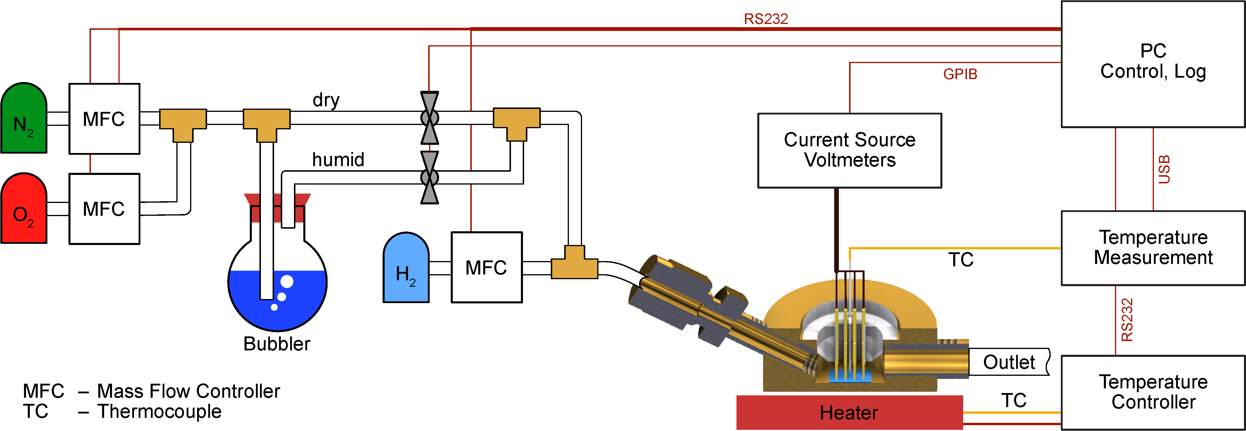
Gas Sensing Testing System Description

Appendix B
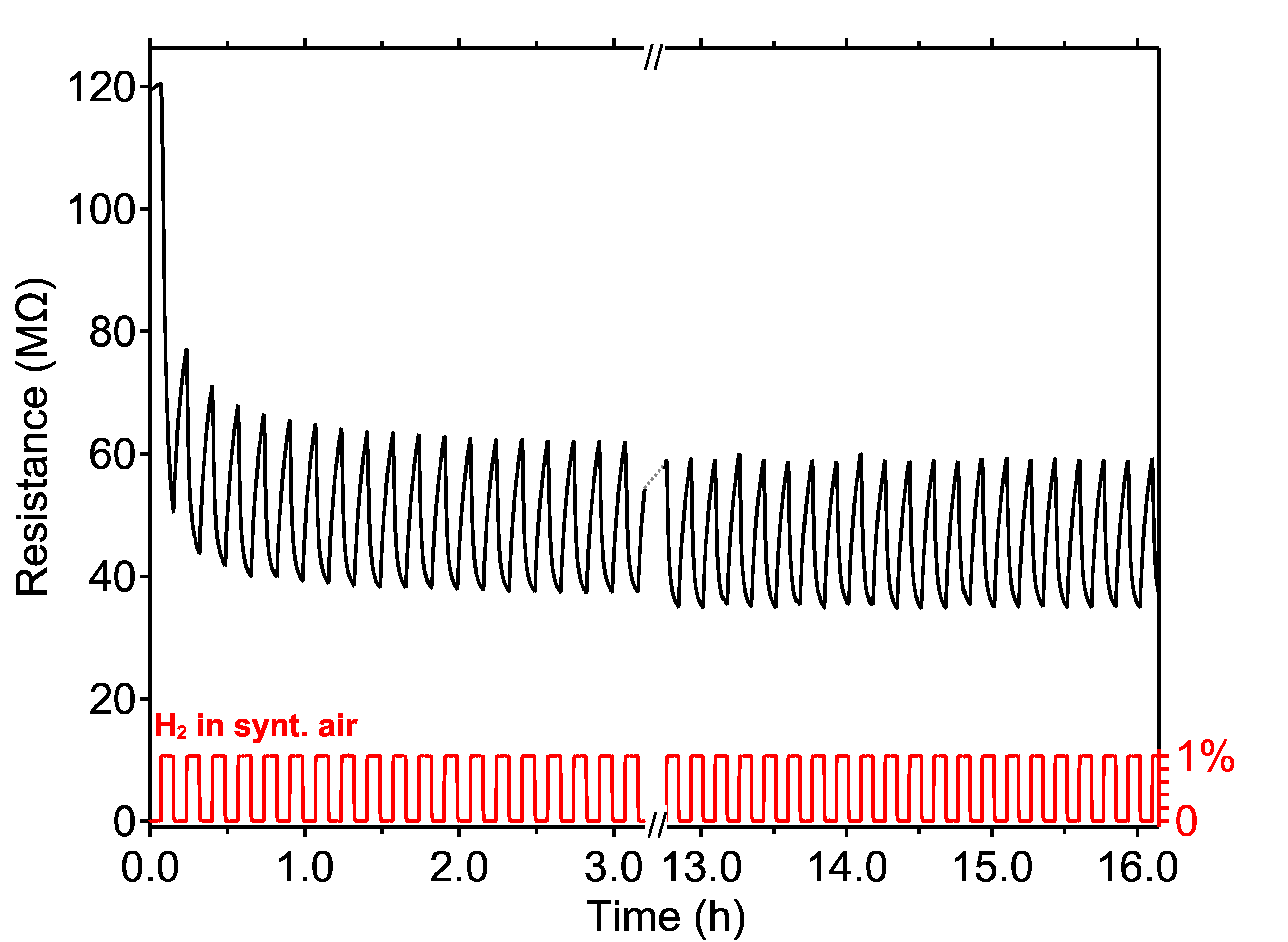
Stabilization Curve

References
- Liu, Y.; Xiao, S.; Du, K. Chemiresistive Gas Sensors Based on Hollow Heterojunction: A Review. Adv. Mater. Interfaces 2021, 8, 1–21. [Google Scholar] [CrossRef]
- Steinhauer, S. Gas sensors based on copper oxide nanomaterials: A review. Chemosensors 2021, 9, 51. [Google Scholar] [CrossRef]
- Nasiri, N.; Clarke, C. Nanostructured chemiresistive gas sensors for medical applications. Sensors 2019, 19, 462. [Google Scholar] [CrossRef] [PubMed] [Green Version]
- Srinivasan, P.; Ezhilan, M.; Kulandaisamy, A.J.; Babu, K.J.; Rayappan, J.B.B. Room temperature chemiresistive gas sensors: Challenges and strategies—A mini review. J. Mater. Sci. Mater. Electron. 2019, 30, 15825–15847. [Google Scholar] [CrossRef]
- Mridha, S.; Basak, D. Investigation of a p-CuO/n-ZnO thin film heterojunction for H2 gas-sensor applications. Semicond. Sci. Technol. 2006, 21, 928–932. [Google Scholar] [CrossRef]
- Liu, Y.; Lai, P.T.; Tang, W.M. Improved hydrogen-sensing performance of Pd/WO3/SiC Schottky diode by La doping. In Proceedings of the 2016 IEEE International Conference on Electron Devices and Solid-State Circuits (EDSSC), Hong Kong, China, 3–5 August 2016; pp. 338–341. [Google Scholar]
- Maziarz, W. TiO2/SnO2 and TiO2/CuO thin film nano-heterostructures as gas sensors. Appl. Surf. Sci. 2019, 480, 361–370. [Google Scholar] [CrossRef]
- Moseley, P.T. Progress in the development of semiconducting metal oxide gas sensors: A review. Meas. Sci. Technol. 2017, 28, 082001. [Google Scholar] [CrossRef]
- Boudiba, A.; Zhang, C.; Olivier, M.; Debliquy, M.; Snyders, R.; Roussel, P. Sensing mechanism of hydrogen sensors based on Pd loaded tungsten oxide (Pd-WO3). In Proceedings of the 14th International Meeting on Chemical Sensors—IMCS 2012, Nuremberg, Germany, 20–23 May 2012; pp. 795–797. [Google Scholar]
- Ghasempour, R.; Mortazavi, S.Z.; Iraji Zad, A.; Rahimi, F. Hydrogen sensing properties of multi-walled carbon nanotube films sputtered by Pd. Int. J. Hydrogen Energy 2010, 35, 4445–4449. [Google Scholar] [CrossRef]
- Haviar, S.; Čapek, J.; Batková, Š.; Kumar, N.; Dvořák, F.; Duchoň, T.; Fialová, M.; Zeman, P. Hydrogen gas sensing properties of WO3 sputter-deposited thin films enhanced by on-top deposited CuO nanoclusters. Int. J. Hydrogen Energy 2018, 43, 22756–22764. [Google Scholar] [CrossRef]
- Mattoni, G.; de Jong, B.; Manca, N.; Tomellini, M.; Caviglia, A.D. Single-Crystal Pt-Decorated WO3 Ultrathin Films: A Platform for Sub-ppm Hydrogen Sensing at Room Temperature. ACS Appl. Nano Mater. 2018, 1, 3446–3452. [Google Scholar] [CrossRef] [Green Version]
- Takahashi, H.; Okazaki, S.; Nishijima, Y.; Arakawa, T. Optimization of Hydrogen Sensing Performance of Pt/WO3 Gasochromic Film Fabricated by Sol–Gel Method. Sens. Mater. 2017, 29, 1259–1268. [Google Scholar]
- Jagadale, S.B.; Patil, V.L.; Vanalakar, S.A.; Patil, P.S.; Deshmukh, H.P. Preparation, characterization of 1D ZnO nanorods and their gas sensing properties. Ceram. Int. 2018, 44, 3333–3340. [Google Scholar] [CrossRef]
- Zappa, D. The influence of Nb on the synthesis of WO3 nanowires and the effects on hydrogen sensing performance. Sensors 2019, 19, 2332. [Google Scholar] [CrossRef] [Green Version]
- Wang, Y.; Cai, L.; Li, Y.; Tang, Y.; Xie, C. Structural and photoelectrocatalytic characteristic of ZnO/ZnWO4/WO3 nanocomposites with double heterojunctions. Phys. E Low-Dimens. Syst. Nanostructures 2010, 43, 503–509. [Google Scholar] [CrossRef]
- Kumar, N.; Haviar, S.; Rezek, J.; Baroch, P.; Zeman, P. Tuning Stoichiometry and Structure of Pd-WO3−x Thin Films for Hydrogen Gas Sensing by High-Power Impulse Magnetron Sputtering. Materials 2020, 13, 5101. [Google Scholar] [CrossRef] [PubMed]
- Zhang, D.; Wu, Z.; Zong, X.; Zhang, Y. Fabrication of polypyrrole/Zn2SnO4 nanofilm for ultra-highly sensitive ammonia sensing application. Sens. Actuators B Chem. 2018, 274, 575–586. [Google Scholar] [CrossRef]
- Leonard, K.C.; Nam, K.M.; Lee, H.C.; Kang, S.H.; Park, H.S.; Bard, A.J. ZnWO4/WO3 composite for improving photoelectrochemical water oxidation. J. Phys. Chem. C 2013, 117, 15901–15910. [Google Scholar] [CrossRef]
- Mohamed, M.M.; Ahmed, S.A.; Khairou, K.S. Unprecedented high photocatalytic activity of nanocrystalline WO3/NiWO4 hetero-junction towards dye degradation: Effect of template and synthesis conditions. Appl. Catal. B Environ. 2014, 150–151, 63–73. [Google Scholar] [CrossRef]
- Zhan, F.; Li, J.; Li, W.; Liu, Y.; Xie, R.; Yang, Y.; Li, Y.; Chen, Q. In situ formation of CuWO4/WO3 heterojunction plates array films with enhanced photoelectrochemical properties. Int. J. Hydrogen Energy 2015, 40, 6512–6520. [Google Scholar] [CrossRef]
- Kumar, N.; Čapek, J.; Haviar, S. Nanostructured CuWO4/WO3-films prepared by reactive magnetron sputtering for hydrogen sensing. Int. J. Hydrogen Energy 2020, 45, 18066–18074. [Google Scholar] [CrossRef]
- Simion, C.E.; Somacescu, S.; Teodorescu, V.S.; Osiceanu, P.; Stanoiu, A. H2S sensing mechanism of SnO2-CuWO4 operated under pulsed temperature modulation. Sens. Actuators B Chem. 2018, 259, 258–268. [Google Scholar] [CrossRef]
- Catto, A.C.; Fiorido, T.; Souza, É.L.S.; Avansi, W.; Andres, J.; Aguir, K.; Longo, E.; Cavalcante, L.S.; da Silva, L.F. Improving the ozone gas-sensing properties of CuWO4 nanoparticles. J. Alloys Compd. 2018, 748, 411–417. [Google Scholar] [CrossRef] [Green Version]
- Zhang, W.; Zhang, D.; Zhang, Y. High-performance NO2 gas sensor based on bimetallic oxide CuWO4 decorated with reduced graphene oxide. J. Mater. Sci. Mater. Electron. 2020, 31, 6706–6715. [Google Scholar] [CrossRef]
- Polyakov, B.; Kuzmin, A.; Vlassov, S.; Butanovs, E.; Zideluns, J.; Butikova, J.; Kalendarev, R.; Zubkins, M. A comparative study of heterostructured CuO/CuWO4 nanowires and thin films. J. Cryst. Growth 2017, 480, 78–84. [Google Scholar] [CrossRef]
- Zheng, J.Y.; Song, G.; Kim, C.W.; Kang, Y.S. Facile preparation of p-CuO and p-CuO/n-CuWO4 junction thin films and their photoelectrochemical properties. Electrochim. Acta 2012, 69, 340–344. [Google Scholar] [CrossRef]
- Andrade Neto, N.F.; Oliveira, Y.G.; Nascimento, J.H.O.; Bomio, M.R.D.; Motta, F.V. Influence of pH variation on CuWO4, CuWO4/WO3 and CuWO4/CuO structures stabilization: Study of the photocatalytic properties under sunlight. J. Mater. Sci. Mater. Electron. 2020, 31, 18221–18233. [Google Scholar] [CrossRef]
- Qi, Q.; Zhang, T.; Zheng, X.; Fan, H.; Liu, L.; Wang, R.; Zeng, Y. Electrical response of Sm2O3-doped SnO2 to C2H2 and effect of humidity interference. Sens. Actuators B Chem. 2008, 134, 36–42. [Google Scholar] [CrossRef]
- Wang, C.; Yin, L.; Zhang, L.; Xiang, D.; Gao, R. Metal Oxide Gas Sensors: Sensitivity and Influencing Factors. Sensors 2010, 10, 2088–2106. [Google Scholar] [CrossRef] [PubMed] [Green Version]
- Miao, J.; Chen, C.; Lin, J.Y.S. Humidity independent hydrogen sulfide sensing response achieved with monolayer film of CuO nanosheets. Sens. Actuators B Chem. 2020, 309, 127785. [Google Scholar] [CrossRef]
- Kumar, A.; Zhang, P.; Vincent, A.; McCormack, R.; Kalyanaraman, R.; Cho, H.J.; Seal, S. Hydrogen selective gas sensor in humid environment based on polymer coated nanostructured-doped tin oxide. Sens. Actuators B Chem. 2011, 155, 884–892. [Google Scholar] [CrossRef]
- Hübert, T.; Boon-Brett, L.; Black, G.; Banach, U. Hydrogen sensors—A review. Sens. Actuators B Chem. 2011, 157, 329–352. [Google Scholar] [CrossRef]
- Moschogiannaki, M.; Zouridi, L.; Sukunta, J.; Phanichphant, S.; Gagaoudakis, E. High performance hydrogen gas sensors based on PdO-decorated p-type CoV2O6 nanoparticles. Sens. Actuators B. Chem. 2020, 324, 128744. [Google Scholar] [CrossRef]
- Khan, F.U.; Mehmood, S.; Liu, S.; Xu, W.; Shah, M.N. A p-n Heterojunction Based Pd/PdO@ZnO Organic Frameworks for Formaldehyde Gas Sensor. Front Chem. 2021, 9, 1–12. [Google Scholar] [CrossRef] [PubMed]
- Moseley, P. Solid state gas sensors. Meas. Sci. Technol. 1997, 223, 223–237. [Google Scholar] [CrossRef]
- Kumari, T.; Gopal, R.; Goyal, A.; Joshi, J. Sol–Gel Synthesis of Pd@PdO Core–Shell Nanoparticles and Effect of Precursor Chemistry on Their Structural and Optical Properties. J. Inorg. Organomet. Polym. Mater. 2019, 29, 316–325. [Google Scholar] [CrossRef]
- Baylet, A.; Marécot, P.; Duprez, D.; Castellazzi, P.; Groppi, G.; Forzatti, P. In situ Raman and in situ XRD analysis of PdO reduction and Pd° oxidation supported on γ-Al2O3 catalyst under different atmospheres. Phys. Chem. Chem. Phys. 2011, 13, 4607–4613. [Google Scholar] [CrossRef]
- Zhu, S.; Liu, Y.; Wu, G.; Fei, L.; Zhang, S.; Hu, Y.; Yan, Z.; Wang, Y.; Gu, H.; Chen, W. Mechanism study on extraordinary room-temperature CO sensing capabilities of Pd-SnO2 composite nanoceramics. Sens. Actuators B Chem. 2019, 285, 49–55. [Google Scholar] [CrossRef]
- Aruna, I.; Mehta, B.R.; Malhotra, L.K.; Shivaprasad, S.M. Size dependence of core and valence binding energies in Pd nanoparticles: Interplay of quantum confinement and coordination reduction. J. Appl. Phys. 2008, 104, 064308. [Google Scholar] [CrossRef] [Green Version]
- Sriyutha Murthy, P.; Venugopalan, V.P.; Das Arunya, D.; Dhara, S.; Pandiyan, R.; Tyagi, A.K. Antibiofilm activity of nano sized CuO. In Proceedings of the International Conference on Nanoscience, Engineering and Technology (ICONSET 2011), Chennai, India, 28–30 November 2011; pp. 580–583. [Google Scholar] [CrossRef]
- Chen, C.; Bi, W.; Xia, Z.; Yuan, W.; Li, L. Hydrothermal Synthesis of the CuWO4/ZnO Composites with Enhanced Photocatalytic Performance. ACS Omega 2020, 5, 13185–13195. [Google Scholar] [CrossRef]
- Thongpan, W.; Louloudakis, D.; Pooseekheaw, P.; Kumpika, T.; Kantarak, E.; Sroila, W.; Panthawan, A.; Thongsuwan, W.; Singjai, P. Porous CuWO4/WO3 composite films with improved electrochromic properties prepared by sparking method. Mater. Lett. 2019, 257, 126747. [Google Scholar] [CrossRef]
- Tayar Galante, M.; Živković, A.; Alvim, J.C.; Calchi Kleiner, C.C.; Sangali, M.; Taylor, S.F.R.; Greer, A.J.; Hardacre, C.; Rajeshwar, K.; Caram, R.; et al. Arc Synthesis, Crystal Structure, and Photoelectrochemistry of Copper(I) Tungstate. ACS Appl. Mater. Interfaces 2021, 13, 32865–32875. [Google Scholar] [CrossRef] [PubMed]
- Gancheva, M.; Velinova, R.; Konova, P.; Stefanov, P.; Iordanova, R.; Naydenov, A. On the stabilization of the oxidized state of palladium by CuWO4 for application as catalyst in abatement of C1–C4 hydrocarbons emissions. Mater. Res. Express 2019, 6, 085554. [Google Scholar] [CrossRef]
- Annanouch, F.E.; Roso, S.; Haddi, Z.; Vallejos, S.; Umek, P.; Bittencourt, C.; Blackman, C.; Vilic, T.; Llobet, E. p-Type PdO nanoparticles supported on n-type WO3 nanoneedles for hydrogen sensing. Thin Solid Films 2016, 618, 238–245. [Google Scholar] [CrossRef]
- Cao, Y.; Zhou, C.; Chen, Y.; Qin, H.; Hu, J. Enhanced CO Sensing Performances of PdO/WO3 Determined by Heterojunction Structure under Illumination. ACS Omega 2020, 5, 28784–28792. [Google Scholar] [CrossRef] [PubMed]
- Urasinska-Wojcik, B.; Gardner, J.W. H2S Sensing in Dry and Humid H2 Environment with p-Type CuO Thick-Film Gas Sensors. IEEE Sens. J. 2018, 18, 3502–3508. [Google Scholar] [CrossRef]
- Jolly Bose, R.; Illyaskutty, N.; Tan, K.S.; Rawat, R.S.; Matham, M.V.; Kohler, H.; Mahadevan Pillai, V.P. Hydrogen sensors based on Pt-loaded WO3 sensing layers. Europhys. Lett. 2016, 114, 66002. [Google Scholar] [CrossRef]
- De Marcellis, A.; Ferri, G.; Mantenuto, P.; Giancaterini, L.; Cantalini, C. WO3 hydrogen resistive gas sensor and its wide-range current-mode electronic read-out circuit. IEEE Sens. J. 2013, 13, 2792–2798. [Google Scholar] [CrossRef]
- Boudiba, A.; Roussel, P.; Zhang, C.; Olivier, M.-G.G.; Snyders, R.; Debliquy, M. Sensing mechanism of hydrogen sensors based on palladium-loaded tungsten oxide (Pd-WO3). Sens. Actuators B Chem. 2013, 187, 84–93. [Google Scholar] [CrossRef]
- Wicker, S.; Guiltat, M.; Weimar, U.; Hémeryck, A.; Barsan, N. Ambient Humidity Influence on CO Detection with SnO2 Gas Sensing Materials. A Combined DRIFTS/DFT Investigation. J. Phys. Chem. C 2017, 121, 25064–25073. [Google Scholar] [CrossRef] [Green Version]
- Ma, S.; Hu, M.; Zeng, P.; Li, M.; Yan, W.; Qin, Y. Synthesis and low-temperature gas sensing properties of tungsten oxide nanowires/porous silicon composite. Sens. Actuators B Chem. 2014, 192, 341–349. [Google Scholar] [CrossRef]
- Yamaguchi, Y.; Imamura, S.; Nishio, K.; Fujimoto, K. Influence of temperature and humidity on the electrical sensing of Pt/WO3 thin film hydrogen gas sensor. J. Ceram. Soc. Jpn. 2016, 124, 629–633. [Google Scholar] [CrossRef] [Green Version]
- Yadav, P.; Kumar, A.; Sanger, A.; Gautam, Y.K.; Singh, B.P.A.L. Sputter-Grown Pd-Capped CuO Thin Films for a Highly Sensitive and Selective Hydrogen Gas Sensor. J. Electron. Mater. 2020, 50, 192–200. [Google Scholar] [CrossRef]
- Rydosz, A.; Czapla, A. CuO and CuO/TiO2-y thin-film gas sensors of H2 and NO2. In Proceedings of the 2018 XV International Scientific Conference on Optoelectronic and Electronic Sensors (COE), Warsaw, Poland, 17–20 June 2018; pp. 2016–2019. [Google Scholar]
- Sarıca, N.; Alev, O.; Arslan, L.Ç.; Öztürk, Z.Z. Characterization and gas sensing performances of noble metals decorated CuO nanorods. Thin Solid Films 2019, 685, 321–328. [Google Scholar] [CrossRef]
- Cretu, V.; Postica, V.; Mishra, A.K.; Hoppe, M.; Tiginyanu, I.; Mishra, Y.K.; Chow, L.; de Leeuw, N.H.; Adelung, R.; Lupan, O. Synthesis, characterization and DFT studies of zinc-doped copper oxide nanocrystals for gas sensing applications. J. Mater. Chem. A 2016, 4, 6527–6539. [Google Scholar] [CrossRef] [Green Version]
- Aygün, S.; Cann, D. Hydrogen sensitivity of doped CuO/ZnO heterocontact sensors. Sens. Actuators B Chem. 2005, 106, 837–842. [Google Scholar] [CrossRef]
- Barreca, D.; Carraro, G.; Comini, E.; Gasparotto, A.; Maccato, C.; Sada, C.; Sberveglieri, G.; Tondello, E. Novel Synthesis and Gas Sensing Performances of CuO–TiO2 Nanocomposites Functionalized with Au Nanoparticles. J. Phys. Chem. C 2011, 115, 10510–10517. [Google Scholar] [CrossRef]


| Sensing Material and Morphology | Sensitivity S | Temperature (°C) | Concentration (ppm) | References | |||
|---|---|---|---|---|---|---|---|
| Value (1) | Definition | ||||||
| Pd/CuWO4/CuO | 8.2 (Dry) 3.4 (Dry) 3.4 (Humid) | Ra/Rg | 80 150 150 | 10,000 | This work | ||
| CuO | CuO film | 1.25 | RH2/Ra | 400 | 125 | A. Rydosz et al. (2018) | [56] |
| CuO/TiO2−y | CuO/TiO2 films | 1.5 | RH2/Ra | 400 | 125 | A. Rydosz et al. (2018) | [56] |
| Pd/CuO | Pd-decorated CuO nanorods | 4.5 | (Ia − Ig)/Ig | 200 | 1000 | N. Sarıca et al. (2019) | [57] |
| CuWO4/WO3 | CuWO4/WO3 heterojunction | 5.0 | (Ra − Rg)/Rg | 350 | 10,000 | Kumar et al. (2020) | [22] |
| Zn/CuO | Zn-doped CuO | 7 (Dry) 3.8 (Humid) | (Rg − Ra)/Ra | 650 | 100 | V. Cretu et al. (2016) | [58] |
| CuO/WO3 | CuO nanoclusters on WO3 | 2.4 | (Ra − Rg)/Rg | 300 | 10,000 | S. Haviar et al. (2018) | [11] |
| CuO/ZnO | CuO/ZnO heterocontacts | 2.3 | IH2/Ia | 400 | 4000 | S. Aygün et at. (2005) | [59] |
| CuO/TiO2 | CuO/TiO2 nanocomposites | 2–3 | (Rg − Ra)/Ra | 200 | 1000 | D. Barreca et al. (2011) | [60] |
| Pd/CuO | Pd-capped CuO thin film | 3.8 (Dry) 3.0 (Humid) | Ra/Rg | 300 | 1000 | P. Yadav et al. (2020) | [55] |
Publisher’s Note: MDPI stays neutral with regard to jurisdictional claims in published maps and institutional affiliations. |
© 2021 by the authors. Licensee MDPI, Basel, Switzerland. This article is an open access article distributed under the terms and conditions of the Creative Commons Attribution (CC BY) license (https://creativecommons.org/licenses/by/4.0/).
Share and Cite
Kumar, N.; Haviar, S.; Zeman, P. Three-Layer PdO/CuWO4/CuO System for Hydrogen Gas Sensing with Reduced Humidity Interference. Nanomaterials 2021, 11, 3456. https://doi.org/10.3390/nano11123456
Kumar N, Haviar S, Zeman P. Three-Layer PdO/CuWO4/CuO System for Hydrogen Gas Sensing with Reduced Humidity Interference. Nanomaterials. 2021; 11(12):3456. https://doi.org/10.3390/nano11123456
Chicago/Turabian StyleKumar, Nirmal, Stanislav Haviar, and Petr Zeman. 2021. "Three-Layer PdO/CuWO4/CuO System for Hydrogen Gas Sensing with Reduced Humidity Interference" Nanomaterials 11, no. 12: 3456. https://doi.org/10.3390/nano11123456