Article

Manipulable Electronic and Optical Properties of Two-Dimensional MoSTe/MoGe2N4 van der Waals Heterostructures

1
School of Physics and Electronics, Shandong Normal University, Jinan 250358, China
2
Shandong Provincial Engineering and Technical Center of Light Manipulations & Institute of Materials and Clean Energy, Shandong Normal University, Jinan 250358, China
*
Authors to whom correspondence should be addressed.
Nanomaterials 2021, 11(12), 3338; https://doi.org/10.3390/nano11123338
Submission received: 5 November 2021 / Revised: 30 November 2021 / Accepted: 6 December 2021 / Published: 8 December 2021
(This article belongs to the Special Issue Two-Dimensional Semiconductor Nanomaterials and Nanodevices)

Abstract

:
van der Waals heterostructures (vdWHs) can exhibit novel physical properties and a wide range of applications compared with monolayer two-dimensional (2D) materials. In this work, we investigate the electronic and optical properties of MoSTe/MoGe2N4 vdWH under two different configurations using the VASP software package based on density functional theory. The results show that Te4-MoSTe/MoGe2N4 vdWH is a semimetal, while S4-MoSTe/MoGe2N4 vdWH is a direct band gap semiconductor. Compared with the two monolayers, the absorption coefficient of MoSTe/MoGe2N4 vdWH increases significantly. In addition, the electronic structure and the absorption coefficient can be manipulated by applying biaxial strains and changing interlayer distances. These studies show that MoSTe/MoGe2N4 vdWH is an excellent candidate for high-performance optoelectronic devices.

1. Introduction

Two-dimensional (2D) materials with different physical properties have been discovered in the last few decades, such as graphene, hexagonal boron nitride (h-BN), layered metal oxides, and transition metal dichalcogenides (TMDs) [1,2,3,4,5]. As one of the research hotspots in 2D materials, TMD materials are promising in nanoelectronics, optoelectronics, and photocatalytic devices [6,7,8,9,10]. TMD monolayers can be expressed as MX2, in which M represents the transition metal atom and X refers to the halogen atom. The lattice structure of TMDs is similar to a “sandwich” structure. The transition metal atom M is sandwiched between two layers of halogen atom X, which are connected by chemical bonds. One layer of the halogen atom X in MX2 can be replaced by another halogen atom Y, which can form a non-centrosymmetric structure and is referred to as Janus materials with the chemical formula Janus MXY [11,12]. Janus MXY have many unique physical properties that distinguish them from conventional 2D materials, including strong in-plane piezoelectric polarization [13], valley splitting [14], Rashba spin splitting [15,16], and good catalytic properties [17]. In recent years, people have conducted a lot of research on Janus MXY for M = Mo, W and X, Y = S, Se, Te, etc. As a typical representative of Janus MXY material, the Janus MoSSe monolayer has been successfully manufactured by replacing the Se atom at the top of the MoSe2 monolayer with the S atom, which provides experimental guidance for the synthesis of many Janus structures [17]. On the other hand, as another example, people have theoretically predicted the electronic, vibrational, elastic, and piezoelectric properties of Janus MoSTe [18]. These features prove the great potential of Janus MXY in electronic and photoelectric applications.
New 2D materials have been continuously explored, and their physical properties and potential applications have been intensively investigated. Recently, a high quality MoSi2N4 monolayer has been successfully fabricated by chemical vapor deposition (CVD) [19], which makes the new 2D material MA2Z4 family attract extensive attention, in which M = Mo, W, V, Nb, Ta, Ti, Zr, Hf, or Cr; A = Si or Ge; and Z = N, P, or As [20]. At present, people have revealed the physical properties of the MA2Z4 monolayer through first principles calculations, such as structural stability, electronic properties, visible absorption coefficient, Rashba spin splitting, carrier mobility, and so on. These findings revealed that the fascinating MA2Z4 families are promising 2D materials for many applications due to their outstanding properties [21,22,23,24,25]. Transition metal nitride (TMN) monolayers in this family, such as MoSi2N4 and MoGe2N4, are promising candidates for optoelectronic nanodevices [26,27,28,29]. Theoretical investigations have been carried out for MA2Z4 monolayer and van der Waals heterostructures (vdWH) based on it. Graphene, C2N, MoS2, and MoSe2 have been selected to build vdWH with MoSi2N4, which paves the way for the design of high-performance photocatalysts and optoelectronic nanodevices in the future [30,31,32,33].
vdWH, which is stacked by two or more layered materials, is one of the research hotspots of 2D materials. Compared with 2D monolayer materials, vdWH can improve electrical properties, light absorption efficiency, catalytic hydrogen production performance, etc. [34,35,36]. Although many vdWHs have been manufactured experimentally or predicted theoretically, research on 2D MA2Z4-based vdWHs is still in its infancy. Here, considering that both Janus MoSTe and MoGe2N4 monolayers are indirect band gap semiconductors [28,37] and both have good absorption coefficients in the visible region, we combine the advantages of these two monolayers and construct different configurations of MoSTe/MoGe2N4 vdWHs. The electronic structure, optical properties, and the effects of the biaxial strains and the interlayer distances are investigated. The calculation shows that a MoSTe/MoGe2N4 vdWH can be a semimetal or a direct band gap semiconductor with different stacking configurations. In addition, the optical absorption of MoSTe/MoGe2N4 vdWH has been greatly improved both in the visible and ultraviolet regions compared with those of the individual monolayers. There are transitions between semimetal and semiconductor when biaxial strains and interlayer distances are changed in MoSTe/MoGe2N4 vdWH. In addition, the compression strain enables MoSTe/MoGe2N4 vdWH to significantly increase the absorption intensity in the visible and ultraviolet regions, while the tensile strain reduces the absorption in the visible region. The construction of the MoSTe/MoGe2N4 vdWH improves the electronic structure and the optical absorption compared to its individual monolayers, and these properties can also be modulated by the strain and interlayer distance. MoSTe/MoGe2N4 vdWH can be widely used in optoelectronic nanodevices.

2. Calculation Methods

All our calculations are based on the first principles approach through density functional theory (DFT), which is implemented using the Vienna Ab-initio Simulation Package (VASP) [38,39]. Taking into account the exchange and other correlation energies, the general gradient approximation (GGA) [40] in the form of Perdew–Burke–Ernzerh (PBE) is used. In addition, the DFT-D3 correction method proposed by Grimme is used in the calculations [41]. For the structural optimization, electronic properties, and optical properties, the k-point in the first Brillouin zone is taken as 6 × 6 × 1 according to the Monkhorst–Pack scheme. In order to avoid the influence of interlayer interactions, a vacuum layer of 20 Å is placed perpendicular to the interface in the z-direction. During the calculation, the plane wave cut-off energy is set to 500 eV. At the same time, in order to fully optimize the atomic structure, the convergence accuracy of the force during relaxation is set to less than 0.01 eV/Å for each atom and 10−6 eV for the energy convergence of electron self-consistency.
Optical propagation through a medium, and the dielectric function is used to describe the absorption coefficient [42,43]. The formula is as follows:
ε ( ω ) = ε 1 ( ω ) + i ε 2 ( ω ) .
Dielectric function ε is made up of two parts, real part ε1 and imaginary part ε2. The real part represents the capacity of the material to store energy, and ε1 is given by the Kramers–Kronig formula:
ε 1 ( ω ) = 1 + 2 π P 0 ε 2 α β ( ω ) ω ω 2 ω 2 + i η d ω
where P represents the principal value of the integral.
The imaginary part ε2 represents the loss factor, which is shown in the following equation:
ε 2 ( ω ) = 4 π 2 e 2 Ω lim q 0 c : v : k 2 ω k δ ( ϵ c k ϵ v k ω ) × u c k + e α q u v k u c k + e β q u v k * .
where Ω stands for the volume, α and β are the Cartesian components, eα and eβ are the unit vectors, υ and c represent matrix elements of the transition from the valence band state (uυk) to the conduction band state (uck), and ϵck and ϵυk denote for the energies of the conduction and the valence band, respectively.
The absorption coefficient α(ω) is derived from the above two equations:
α ( ω ) = 2 ω c { [ ε 1 2 ( ω ) + ε 2 2 ( ω ) ] 1 2 ε 1 ( ω ) } 1 2 .

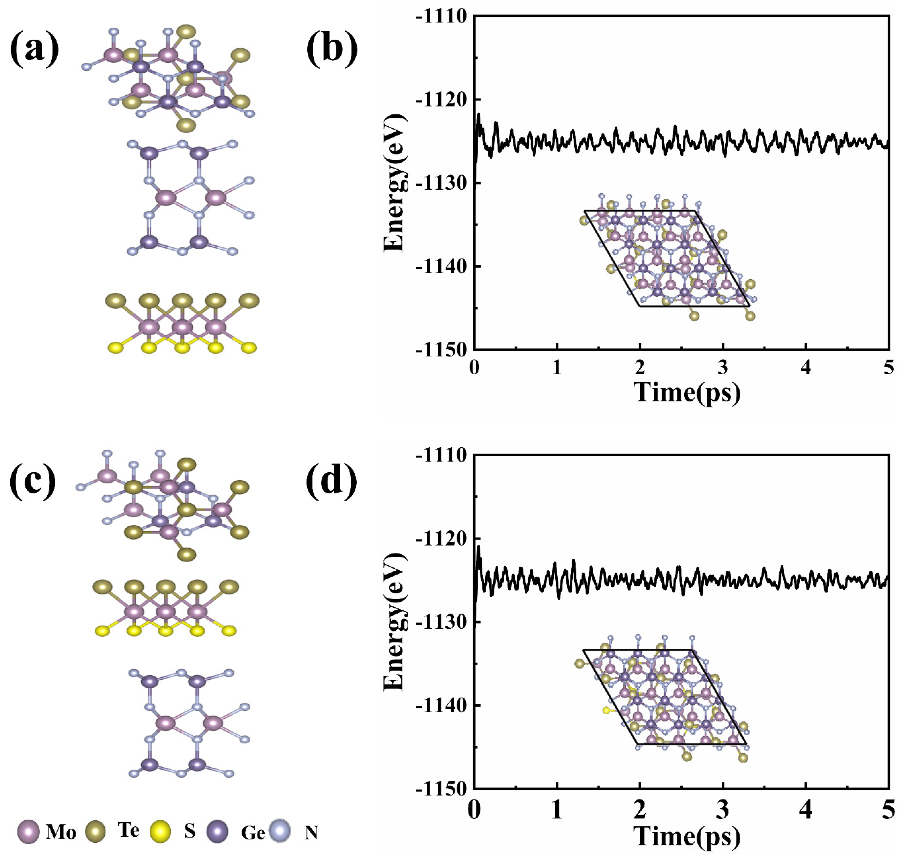
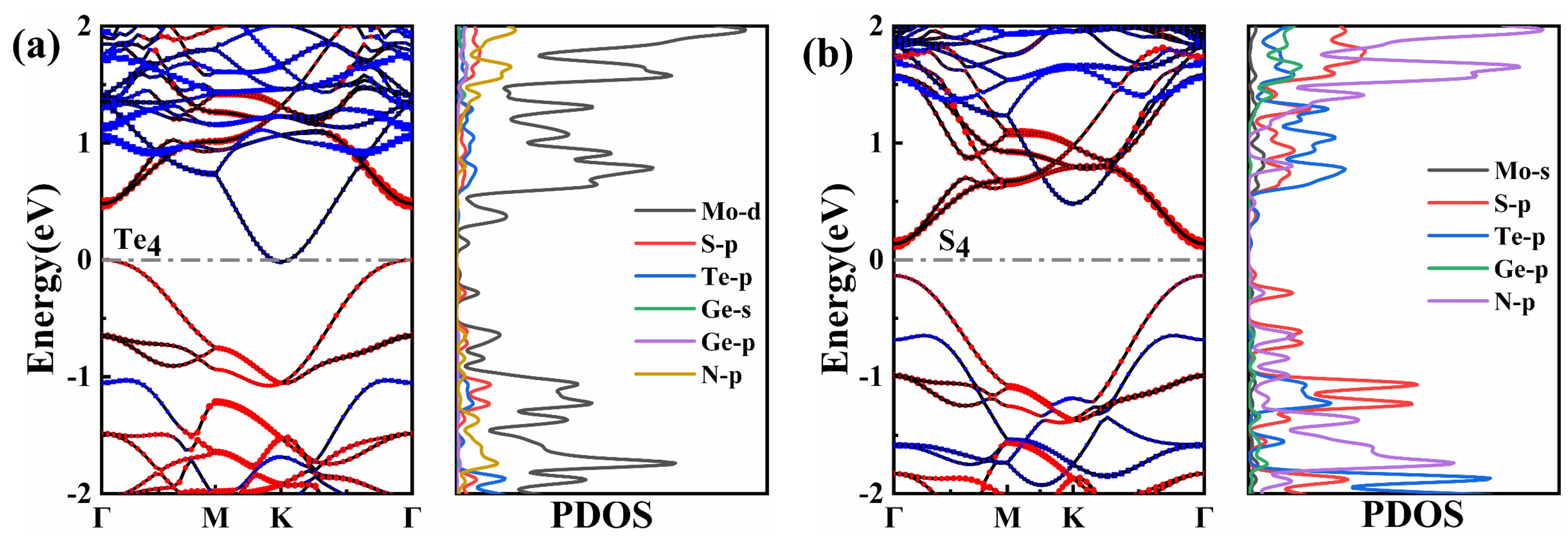
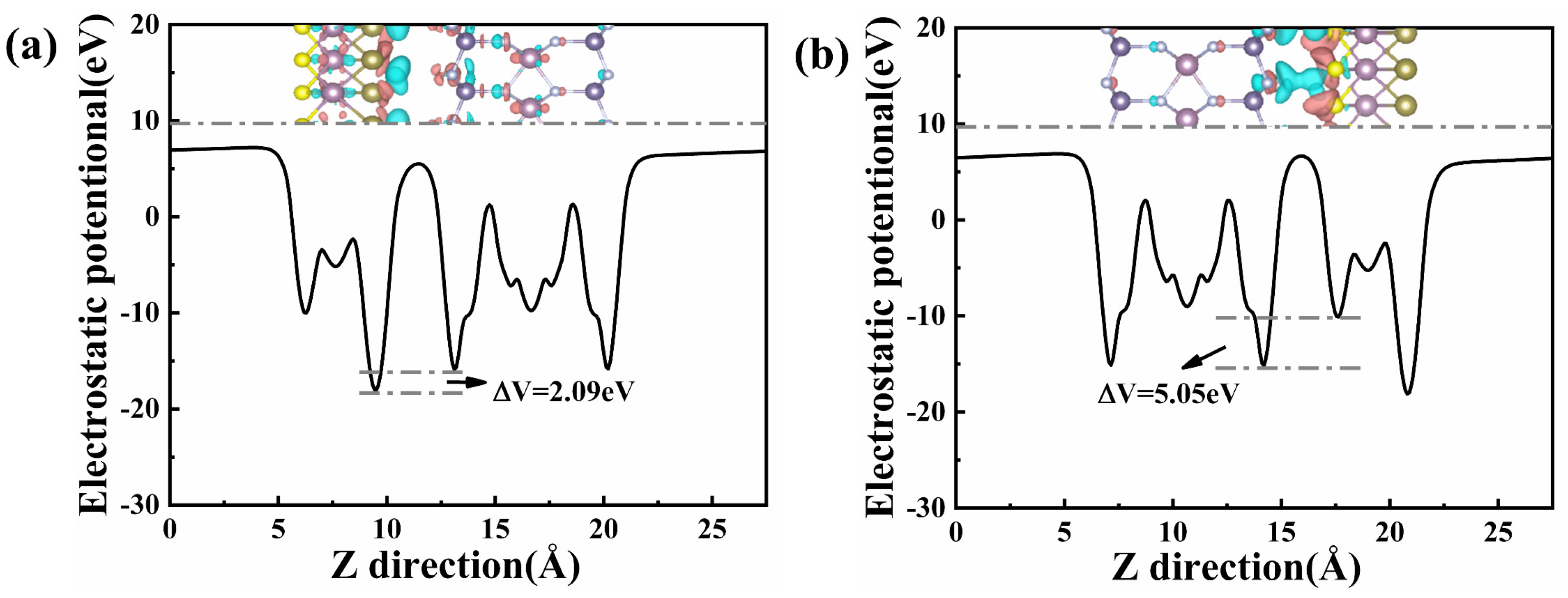
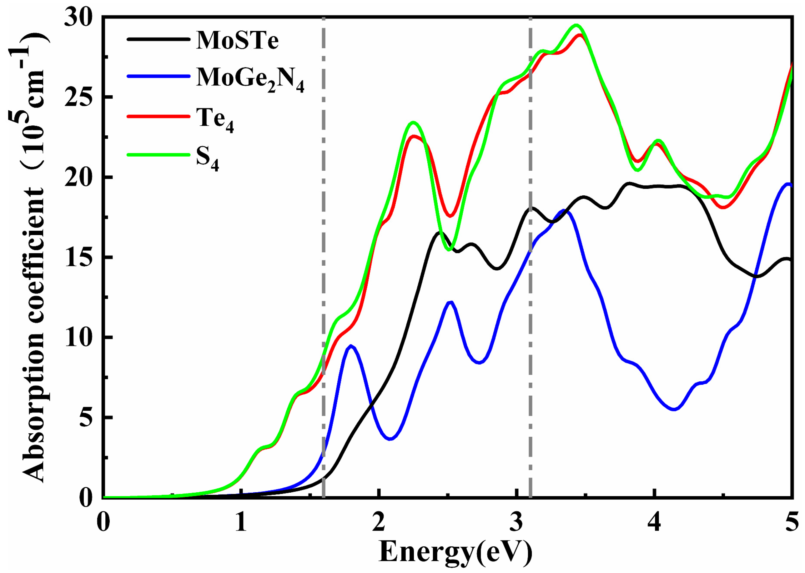
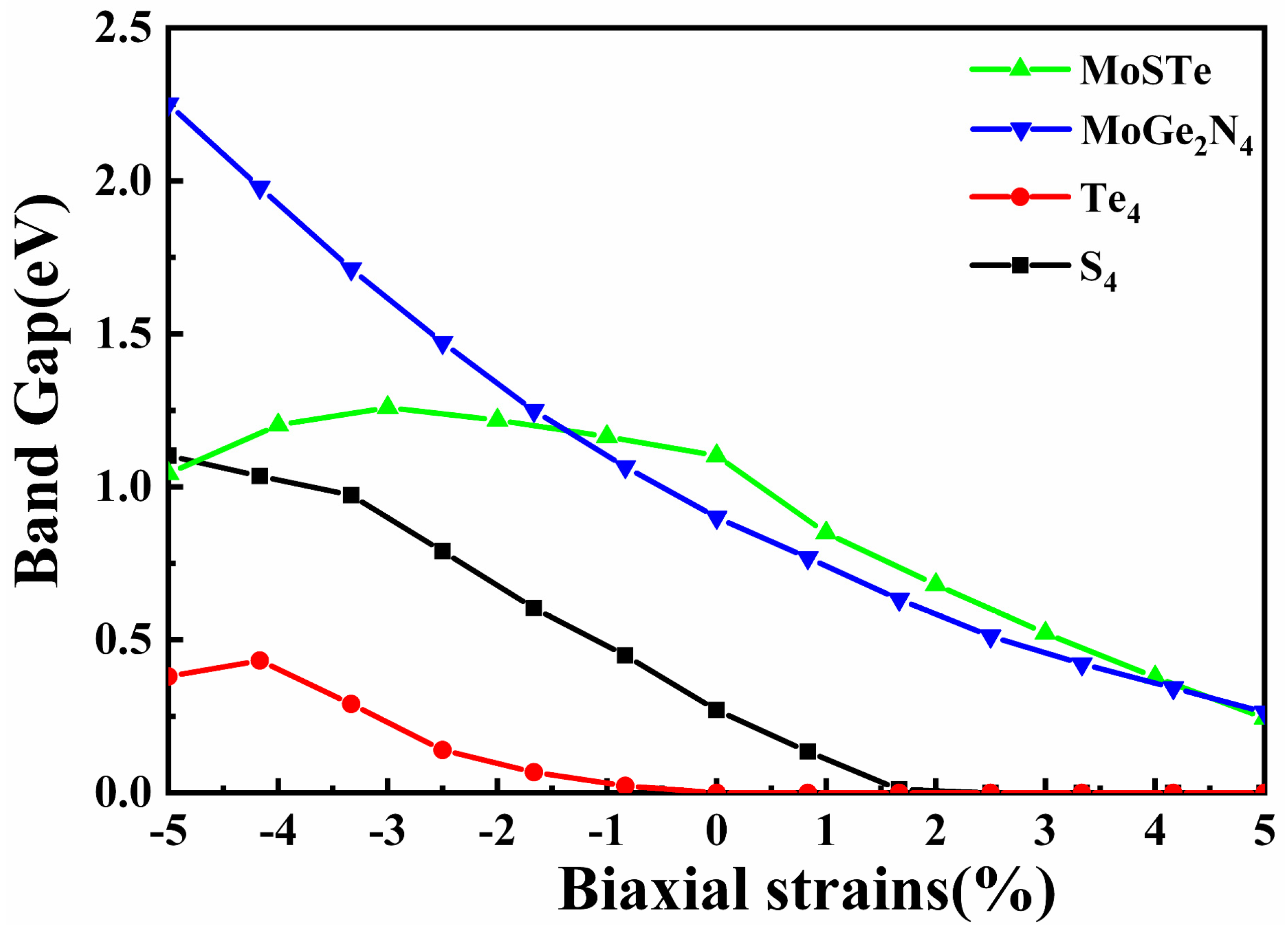
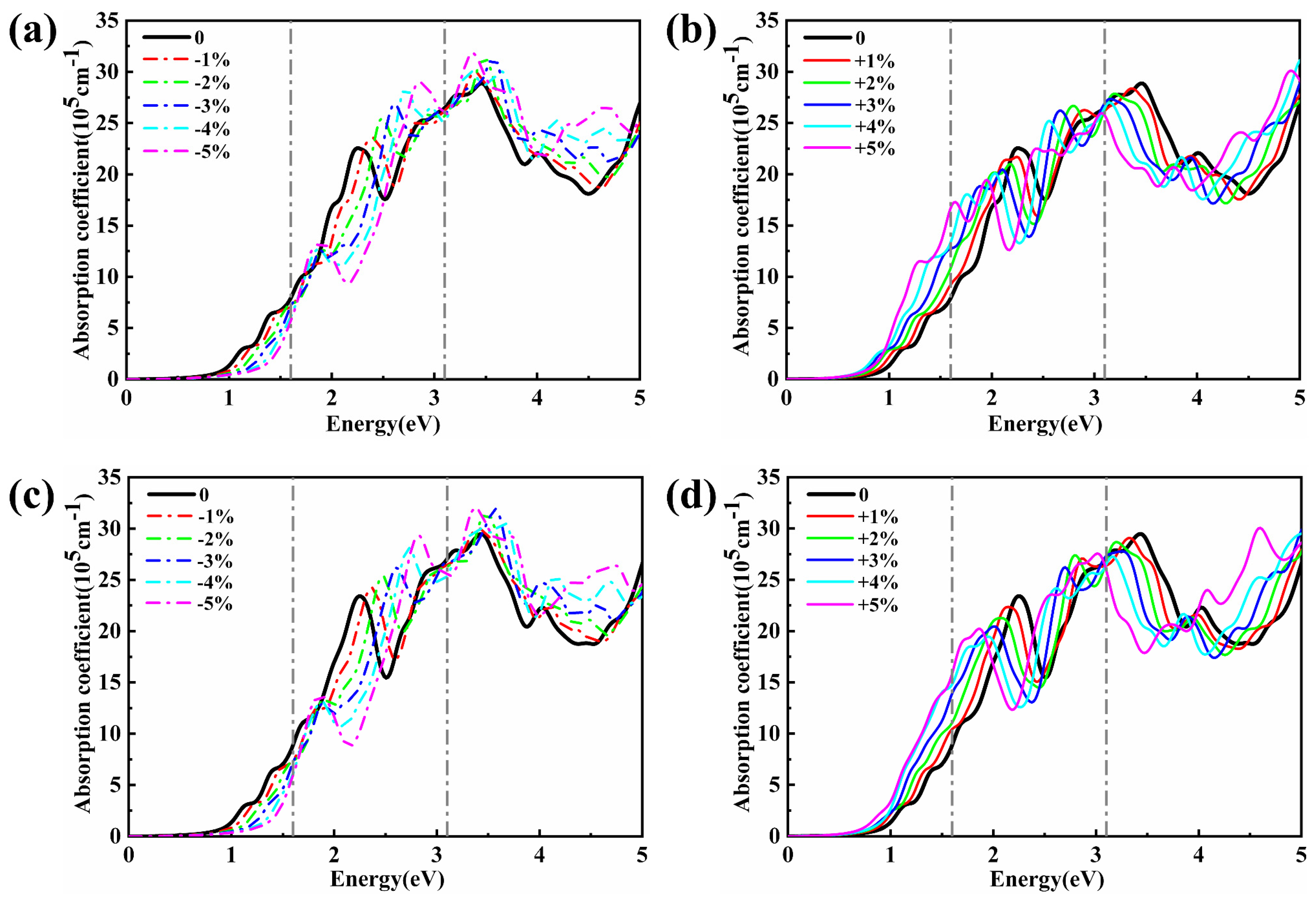
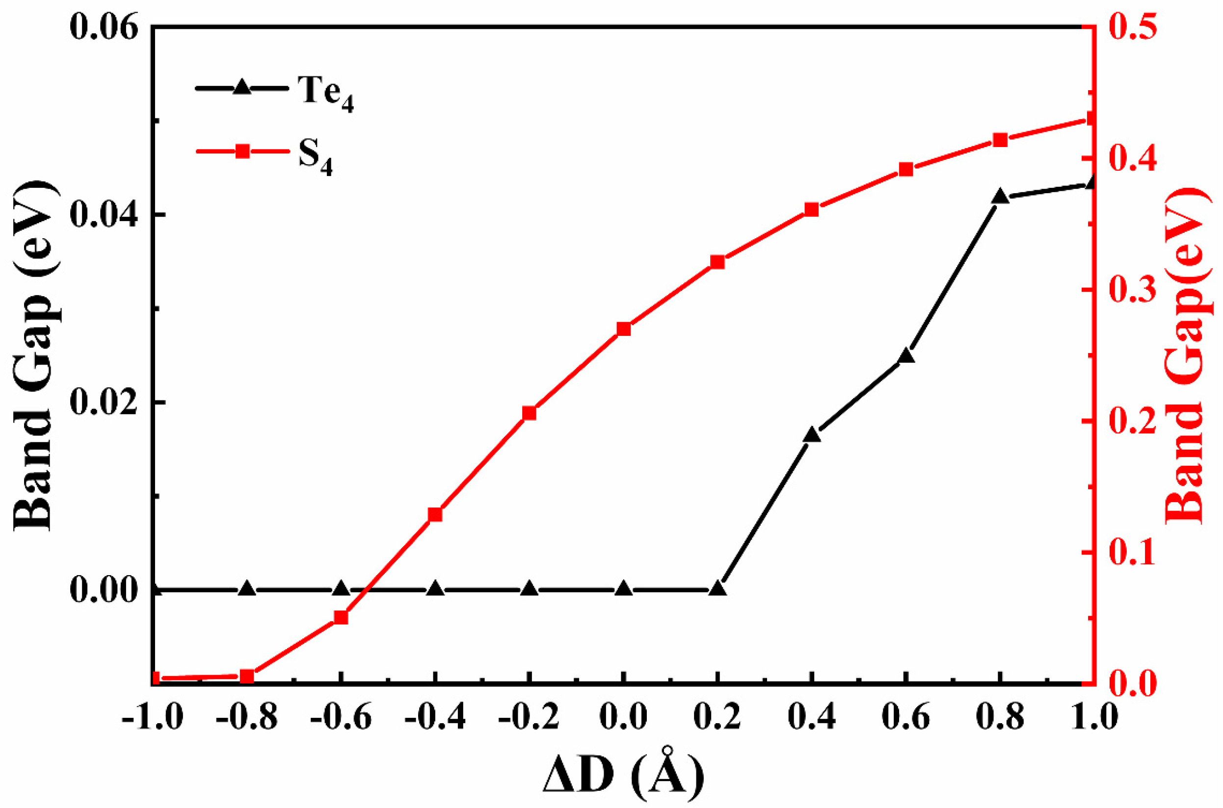
3. Results and Discussions

Before studying the properties of MoSTe/MoGe2N4 vdWH, we first investigate the atomic structure and the electronic characteristics of the two monolayers. In Figure S1, both monolayers of Janus MoSTe and MoGe2N4 are semiconductors. As shown in Figure S1a, the Janus MoSTe monolayer shows a hexagonal atomic structure with the space group P6m1. The Mo atom is connected to the S and Se atoms on each side by covalent bonds. The optimized lattice parameters are a = b = 3.362 Å, the Mo-S bond length is dMo-s = 2.437 Å, and the Mo-Te bond length is dMo-Te = 2.718 Å. At the same time, the conduction band minimum (CBM) of the Janus MoSTe monolayer appears at the K point, while the valence band maximum (VBM) appears at the Γ point, and the indirect band gap is 1.027 eV. The results are consistent with previous reports [37]. The projected density of states (PDOS) of the Janus MoSTe monolayer is shown in Figure S1a. The CBM mainly comes from the strong hybridization between Mo-d, Te-p, and S-p orbitals, while the VBM is contributed from Mo-d and S-p orbitals. Similarly, the MoGe2N4 monolayer has a hexagonal crystal structure with space group P6m1. Atoms in the MoGe2N4 monolayers are connected to each other by covalent bonds in the order of N-Ge-N-Mo-N-Ge-N, so MoGe2N4 can be regarded as MoN2 layers sandwiched between two Ge-N bilayers. The optimized MoGe2N4 monolayers have lattice constants of a = b = 3.037 Å; the bond length of the Mo-N bond is dMo-N = 2.130 Å, and it is dSi-N = 1.892 Å for the Si-N bond. As shown in Figure S1b, the MoGe2N4 monolayer is a semiconductor with an indirect band gap of 0.901 eV. Its CBM is located at the K point and is mainly contributed from Mo-d orbitals, while the VBM is located in the K-Γ path in the 2D hexagonal Brillouin zone and mainly comes from strong hybridization between Mo-d, N-p, and Ge-s orbitals. These results are consistent with the previously reported results [22].
MoSTe/MoGe2N4 vdWH is constructed by a 3 × 3 Janus MoSTe supercell and 2 × 2 MoGe2N4 supercell, and the lattice mismatch value is 1.48% in this case. The stacking modes are named Ten vdWH when the Te atoms of Janus MoSTe are close to the MoGe2N4 layer. Similarly, the stacking method is named Sn vdWH when the S atom of Janus MoSTe is close to the MoGe2N4 layer. There are six possible stacking configurations for Ten and Sn, respectively, so there are twelve different stacking configurations, which are shown in Figure S2. To check the stability of these different stacking configurations, we calculate their binding energies. The binding energy can be expressed as E b = E total E MoSTe E MoGe 2 N 4 , where Etotal, EMoSTe, and EMoGe2N4 are the total energies of the MoSTe/MoGe2N4 vdWH, the Janus MoSTe, and the MoGe2N4 monolayer, respectively. The binding energies for the twelve stacking configurations are listed in Table S1. All binding energies are negative, which indicates that the twelve stacking configurations are stable. The binding energies of Te4 and S4 are lowest compared with the others, which means that these two stacking configurations are the most stable. Therefore, in the subsequent calculations, we focus on Te4 and S4, which are shown in Figure 1. We calculate the ab initio molecular dynamics (AIMD) of Te4 and S4 at 300 K with a simulation duration of 5 ps and a time step of 1 fs. As shown in Figure 1, it is found that the fluctuation of energies is small, which indicates that the two configurations are stable.
As shown in Figure 2, based on the orbital characteristics, we plot the energy band structure and the PDOS of the vdWH using different color plots. It can be found that different stacking patterns can produce different electronic structures due to different interlayer coupling effects. Figure 2a shows the Te4-MoSTe/MoGe2N4 stacked conformation. There is no band gap in Te4-MoSTe/MoGe2N4 vdWH. Its CBM is located at point Γ, mainly coming from the contribution of the MoGe2N4 monolayer, and VBM is located at point K, mainly coming from the contribution of the Janus MoSTe monolayer. This vdWH has a non-overlapping band gap between the two semiconductors, which is crossed through the vdWH by band-to-band quantum tunneling and charge transfer. Therefore, the Te4-MoSTe/MoGe2N4 vdWH is a semimetal, which can be widely used in the design of various high-speed and low-power devices [44]. It can be seen from PDOS that CBM mainly comes from N-p orbitals and VBM mainly comes from S-p orbitals. Figure 2b shows the S4-MoSTe/MoGe2N4 vdWH stacked configuration, and it is clear that S4-MoSTe/MoGe2N4 vdWH has a direct band gap of 0.27 eV, where both CBM and VBM are located at the Γ point. It can be seen that the CBM and VBM come from the contributions of the Janus MoSTe monolayer and the MoGe2N4 monolayer, respectively. It can be seen from the PDOS that the CBM is mainly from the Mo-s orbital and the VBM is mainly from the S-p orbital. This direct band gap semiconductor of S4-MoSTe/MoGe2N4 vdWH can effectively facilitate the separation of electrons and holes in real space. Therefore, this finding makes MoSTe/MoGe2N4 vdWH a promising candidate for the fabrication of high-performance optoelectronic devices with suppressed carrier complexation.
Figure 3 shows the electrostatic potential and differential charge density for two stacked configurations of MoSTe/MoGe2N4 vdWH. The electrostatic potential can reflect the difficulty of the electron transport system and has an impact on the electrical properties of the material. As can be seen from Figure 3, the electrostatic potentials of the two stacking configurations are slightly different. The electrostatic potential of the Janus MoSTe monolayer is deeper than that of the MoGe2N4 monolayer. The electrostatic potential of Te4-MoSTe/MoGe2N4 vdWH decreases by 2.09 eV, while the electrostatic potential of S4-MoSTe/MoGe2N4 vdWH decreases by 5.05 eV. Therefore, there is a built-in electric field between the two layers with the direction from the Janus MoSTe layer to the MoGe2N4 layer, which affects the charge injection and the carrier motion to some extent.
In order to visualize the charge transfer of MoSTe/MoGe2N4 vdWH, we calculate the charge density difference as follows:
Δ ρ = ρ MoSTe / MoGe 2 N 4 ρ MoSTe ρ MoGe 2 N 4
where ρMoSTe/MoGe2N4, ρMoSTe, and ρMoGe2N4 denote the charge density of MoSTe/MoGe2N4 vdWH, Janus MoSTe, and MoGe2N4 monolayer, respectively. In Figure 3, the pink represents electron accumulation and blue represents electron depletion. For Te4-MoSTe/MoGe2N4 vdWH, the electrons are gathered around the Mo atoms in Janus MoSTe and MoGe2N4 layers, and there is no electron transfer between the two layers, as shown in Figure 3a. From Figure 3b, we can clearly see the electron distribution between the two monolayers in S4-MoSTe/MoGe2N4 vdWH. We observe that the electron accumulates in the Janus MoSTe layer, while there is an electron depletion in the MoGe2N4 layer. This shows that the electron is transferred from the MoGe2N4 layer to the Janus MoSTe layer. By Bader charge analysis, we found that only a small amount of 0.575 eV electrons are transferred from the Janus MoSTe layer to the MoGe2N4 layer.
Figure 4 shows the calculated optical absorption spectrum of Janus MoSTe, MoGe2N4, Te4-MoSTe/MoGe2N4 vdWH, and S4-MoSTe/MoGe2N4 vdWH. In the visible region (1.6 eV < E < 3.1 eV), both the Janus MoSTe monolayer and MoGe2N4 monolayer have a high absorption coefficient. Combining the advantages of the two monolayers, the absorption coefficient is significantly increased after the vdWH is formed. Compared with the two independent monolayers, both Te4-MoSTe/MoGe2N4 vdWH and S4-MoSTe/MoGe2N4 vdWH show stronger absorption coefficients. In the ultraviolet (UV) region, the absorption intensity has a maximum. Due to interlayer coupling between Janus MoSTe and MoGe2N4 monolayers, the band gap of MoSTe/MoGe2N4 vdWH is reduced and charge transfer takes place, resulting in an enhanced absorption spectrum. Thus, MoSTe/MoGe2N4 vdWH has a higher optical response and is more favorable for applications in optoelectronic devices compared with monolayers.
Thus far, researchers have found that by applying external stress, it is possible not only to change the electronic properties of two-dimensional materials but also to achieve modulation of the absorption coefficient. In the following study, biaxial strains are applied to Te4-MoSTe/MoGe2N4 vdWH and S4-MoSTe/MoGe2N4 vdWH, and both their electronic and optical properties are investigated. The equations for calculating the strain magnitude of the materials are as follows [45]: ε = [ ( a a 0 ) / a 0 ] × 100 % , where a and a0 represent the lattice constants for applied and unapplied stress, respectively. ε < 0 means compressive stress, and ε > 0 means tensile stress. Stress of −5% ≤ ε ≤ 5% is applied to Te4-MoSTe/MoGe2N4 vdWH and S4-MoSTe/MoGe2N4 vdWH, respectively. The variation of band gap with biaxial strain for the Janus MoSTe monolayer, MoGe2N4 monolayer, and MoSTe/MoGe2N4 vdWH is shown in Figure 5.
The formed MoSTe/MoGe2N4 vdWH has a significantly smaller band gap compared with those of the Janus MoSTe and the MoGe2N4 monolayer. Te4-MoSTe/MoGe2N4 vdWH still shows metallicity, and there is no band gap when tensile strain is applied. However, with increasing compressive strain, the band gap of Te4-MoSTe/MoGe2N4 vdWH gradually increases from zero, and the electronic structure changes from semimetal to semiconductor. When the compressive strain is greater than −5%, the band gap starts to decrease again. At this time, its CBM and VBM are coming from the MoGe2N4 monolayer and Janus MoSTe monolayer, respectively, as shown in Figure S3. The band gap of S4-MoSTe/MoGe2N4 vdWH increases with increasing compressive strain and decreases with increasing tensile strain. However, when a biaxial strain larger than +2% is applied, there is no band gap and S4-MoSTe/MoGe2N4 vdWH becomes a semimetal. Therefore, the electronic structure of MoSTe/MoGe2N4 vdWH can be regulated to change between semimetal and semiconductor by applying biaxial strain.
The optical properties of MoSTe/MoGe2N4 vdWH also change after the biaxial strain is applied. As shown in Figure 6, we investigate the variation patterns of the absorption coefficients of Te4-MoSTe/MoGe2N4 vdWH and S4-MoSTe/MoGe2N4 vdWH with biaxial strain. It is found that the effects of biaxial strain on the absorption intensity of the two vdWHs are basically the same pattern. When compressive strain is applied, the absorption coefficient of MoSTe/MoGe2N4 vdWH decreased with increasing compressive intensity and increased with increasing tensile intensity in the infrared region. In the visible and UV regions, the absorption coefficient of MoSTe/MoGe2N4 vdWH increases with increasing compressive strength and decreases with increasing tensile strength. It can be seen that compressive strain increases the absorption coefficient of MoSTe/MoGe2N4 vdWH in the visible and UV regions, while tensile strain increases the absorption coefficient of the vdWH in the infrared region. Therefore, biaxial strain can also effectively manipulate the absorption properties of MoSTe/MoGe2N4 vdWH.
The variations of the band gaps with different interlayer distances for Te4-MoSTe/MoGe2N4 and S4-MoSTe/MoGe2N4 vdWH are shown in Figure 7, where the equilibrium interlayer distances are 3.4 Å and 3.1 Å, respectively. We find that there is no band gap in Te4-MoSTe/MoGe2N4 vdWH when the interlayer distance is less than 3.63 Å. When the interlayer distance is larger than 3.63 Å, the band gap of Te4-MoSTe/MoGe2N4 vdWH increases with an increase in the interlayer distance. The Te4-MoSTe/MoGe2N4 vdWH changes between semimetal and indirect band gap semiconductors when the interlayer distance changes. The weight band structures of Te4-MoSTe/MoGe2N4 and S4-MoSTe/MoGe2N4 vdWH at different interlayer distances are depicted in Figure S4. We find that the band gap in S4-MoSTe/MoGe2N4 vdWH increases with an increasing interlayer distance and decreases with a decreasing interlayer distance. When the interlayer distance is less than 2.3 Å, the band gap of the S4-MoSTe/MoGe2N4 vdWH becomes small and close to zero. The results indicate that changing the interlayer distance can also regulate the electronic structure of the MoSTe/MoGe2N4 vdWH.

4. Conclusions

In conclusion, we systematically researched the atomic structure, electronic properties, and optical properties of MoSTe/MoGe2N4 vdWH using the VASP software package based on density functional theory. Two monolayers of Janus MoSTe and MoGe2N4 are stacked into heterostructures by van der Waals forces. The thermodynamic stability of MoSTe/MoGe2N4 vdWH is examined using AIMD simulations. Two stacking modes have low binding energies, i.e., Te4-MoSTe/MoGe2N4 vdWH and S4-MoSTe/MoGe2N4 vdWH. Compared with the two separate monolayers, the band gap of MoSTe/MoGe2N4 vdWH is reduced and the light absorption intensity is significantly increased. The energy band structure of MoSTe/MoGe2N4 vdWH can be manipulated by applying a biaxial strain, and the transition between semimetal and semiconductor appears when the biaxial strain changes from −5% to +5%. At the same time, the applied strain can also modulate the light absorption intensity. In the visible and UV regions, the absorption coefficient increases with increasing compressive strain and decreases with increasing tensile strain. In addition, different interlayer distances contribute to a change in the band gap, and a shift between semiconductor and semimetal can be realized. In other words, the electronic and optical properties of MoSTe/MoGe2N4 vdWH can be manipulated by external conditions, such as applying external strain and changing the interlayer distances. Our research has shown that MoSTe/MoGe2N4 vdWH is a potential candidate for high-performance optoelectronic nanodevices.

Supplementary Materials

The following are available online at https://www.mdpi.com/article/10.3390/nano11123338/s1, Figure S1: Band structures and PDOS of (a) Janus MoSTe monolayer and (b) MoGe2N4 monolayer. The Fermi levels are set to zero, Figure S2: The optimized top and side views of MoSTe/MoGe2N4 vdWH for twelve different stacking patterns, Figure S3: Band structures of (a) (b) Te4-MoSTe/MoGe2N4 vdWH and (c) (d) S4-MoSTe/MoGe2N4 vdWH under biaxial strain. Red and blue represent the weights from Janus MoSTe and MoGe2N4 monolayers, respectively. Negative and positive values mean compressive stress and tensile stress, Figure S4: Band structures of (a) (b) Te4-MoSTe/MoGe2N4 vdWH and (c) (d) S4-MoSTe/MoGe2N4 vdWH under different interlayer distances, where the equilibrium interlayer distances are 3.4 Å and 3.1Å, respectively. Red and blue represent the weights from Janus MoSTe and MoGe2N4 monolayers, respectively, Table S1: Binding energies (Eb) of the optimized MoSTe/MoGe2N4 vdWH for the twelve different stacking patterns.

Author Contributions

Writing—original draft preparation, J.W.; writing—review and editing, X.Z.; formal analysis, G.H.; supervision, J.R.; project administration, X.Y. All authors have read and agreed to the published version of the manuscript.

Funding

This research was funded by the National Natural Science Foundation of China, grant Nos. 11674197 and 11974215 and the Natural Science Foundation of Shandong Province, grant No. ZR2021MA105.

Data Availability Statement

The data are available on request from the corresponding author.

Conflicts of Interest

The authors declare no conflict of interest.

References

  1. Yuan, S.; Pang, S.-Y.; Hao, J. 2D transition metal dichalcogenides, carbides, nitrides, and their applications in supercapacitors and electrocatalytic hydrogen evolution reaction. Appl. Phys. Rev. 2020, 7, 021304. [Google Scholar] [CrossRef]
  2. Zavabeti, A.; Jannat, A.; Zhong, L.; Haidry, A.A.; Yao, Z.; Ou, J.Z. Two-Dimensional Materials in Large-Areas: Synthesis, Properties and Applications. Nano-Micro Lett. 2020, 12, 66. [Google Scholar] [CrossRef] [PubMed] [Green Version]
  3. Chaves, A.; Azadani, J.G.; Alsalman, H.; da Costa, D.R.; Frisenda, R.; Chaves, A.J.; Song, S.H.; Kim, Y.D.; He, D.; Zhou, J.; et al. Bandgap engineering of two-dimensional semiconductor materials. npj 2D Mater. Appl. 2020, 4, 28. [Google Scholar] [CrossRef]
  4. Khan, K.; Tareen, A.K.; Aslam, M.; Wang, R.; Zhang, Y.; Mahmood, A.; Ouyang, Z.; Zhang, H.; Guo, Z. Recent developments in emerging two-dimensional materials and their applications. J. Mater. Chem. C 2020, 8, 387–440. [Google Scholar] [CrossRef]
  5. Kumar, R.; Sahoo, S.; Joanni, E.; Singh, R.K.; Yadav, R.M.; Verma, R.K.; Singh, D.P.; Tan, W.K.; del Pino, A.P.; Moshkalev, S.A.; et al. A review on synthesis of graphene, h-BN and MoS2 for energy storage applications: Recent progress and perspectives. Nano Res. 2019, 12, 2655–2694. [Google Scholar] [CrossRef]
  6. Carvalho, A.; Ribeiro, R.M.; Neto, A.H.C. Band nesting and the optical response of two-dimensional semiconducting transition metal dichalcogenides. Phys. Rev. B 2013, 88, 115205. [Google Scholar] [CrossRef] [Green Version]
  7. Ruppert, C.; Aslan, O.B.; Heinz, T.F. Optical Properties and Band Gap of Single- and Few-Layer MoTe2 Crystals. Nano Lett. 2014, 14, 6231–6236. [Google Scholar] [CrossRef] [PubMed]
  8. Tedstone, A.A.; Lewis, D.J.; O’Brien, P. Synthesis, Properties, and Applications of Transition Metal-Doped Layered Transition Metal Dichalcogenides. Chem. Mater. 2016, 28, 1965–1974. [Google Scholar] [CrossRef]
  9. Qiu, B.; Zhao, X.W.; Hu, G.C.; Yue, W.W.; Yuan, X.B.; Ren, J.F. Tuning optical properties of Graphene/WSe2 heterostructure by introducing vacancy: First principles calculations. Phys. E Low Dimens. Syst. Nanostruct. 2020, 116, 113729. [Google Scholar] [CrossRef]
  10. Li, R.; Li, L.-J.; Cheng, Y.; Huang, W. Recent Advances in van der Waals Heterojunctions Based on Semiconducting Transition Metal Dichalcogenides. Adv. Electron. Mater. 2018, 4, 1800270. [Google Scholar] [CrossRef]
  11. Xia, C.; Xiong, W.; Du, J.; Wang, T.; Peng, Y.; Li, J. Universality of electronic characteristics and photocatalyst applications in the two-dimensional Janus transition metal dichalcogenides. Phys. Rev. B 2018, 98, 165424. [Google Scholar] [CrossRef]
  12. Zhang, X.; Lai, Z.; Ma, Q.; Zhang, H. Novel structured transition metal dichalcogenide nanosheets. Chem. Soc. Rev. 2018, 47, 3301–3338. [Google Scholar] [CrossRef] [PubMed]
  13. Dong, L.; Lou, J.; Shenoy, V.B. Large In-Plane and Vertical Piezoelectricity in Janus Transition Metal Dichalchogenides. ACS Nano 2017, 11, 8242–8248. [Google Scholar] [CrossRef]
  14. Zhao, X.; Liu, F.; Ren, J.; Qu, F. Valleytronic and magneto-optical properties of Janus and conventional TiBrI/CrI3 and TiX2/CrI3 (X = Br, I) heterostructures. Phys. Rev. B 2021, 104, 085119. [Google Scholar] [CrossRef]
  15. Chen, J.; Wu, K.; Ma, H.; Hu, W.; Yang, J. Tunable Rashba spin splitting in Janus transition-metal dichalcogenide monolayers via charge doping. RSC Adv. 2020, 10, 6388–6394. [Google Scholar] [CrossRef] [Green Version]
  16. Yao, Q.-F.; Cai, J.; Tong, W.-Y.; Gong, S.-J.; Wang, J.-Q.; Wan, X.; Duan, C.-G.; Chu, J.H. Manipulation of the large Rashba spin splitting in polar two-dimensional transition-metal dichalcogenides. Phys. Rev. B 2017, 95, 165401. [Google Scholar] [CrossRef] [Green Version]
  17. Lai, X.; Zhang, Y.; Zheng, Y.; Xiang, X.; Ye, H.; Liu, W.; Liu, Y. Catalytic activity for hydrogen evolution reaction in square phase Janus MoSSe monolayer: A first-principles study. Phys. Low Dimens. Syst. Nanostruct. 2021, 126, 114485. [Google Scholar] [CrossRef]
  18. Yagmurcukardes, M.; Sevik, C.; Peeters, F.M. Electronic, vibrational, elastic, and piezoelectric properties of monolayer Janus MoSTe phases: A first-principles study. Phys. Rev. B 2019, 100, 045415. [Google Scholar] [CrossRef]
  19. Hong, Y.-L.; Liu, Z.; Wang, L.; Zhou, T.; Ma, W.; Xu, C.; Feng, S.; Chen, L.; Chen, M.-L.; Sun, D.-M.; et al. Chemical vapor deposition of layered two-dimensional MoSi2N4 materials. Science 2020, 369, 670–674. [Google Scholar] [CrossRef] [PubMed]
  20. Novoselov, K.S. Discovery of 2D van der Waals layered MoSi2N4 family. Natl. Sci. Rev. 2020, 7, 1842–1844. [Google Scholar] [CrossRef]
  21. Chen, J.; Tang, Q. The Versatile Electronic, Magnetic and Photo-Electro Catalytic Activity of a New 2D MA2Z4 Family**. Chem. Eur. J. 2021, 27, 9925–9933. [Google Scholar] [CrossRef]
  22. Mortazavi, B.; Javvaji, B.; Shojaei, F.; Rabczuk, T.; Shapeev, A.V.; Zhuang, X. Exceptional piezoelectricity, high thermal conductivity and stiffness and promising photocatalysis in two-dimensional MoSi2N4 family confirmed by first-principles. Nano Energy 2021, 82, 105716. [Google Scholar] [CrossRef]
  23. Wang, L.; Shi, Y.; Liu, M.; Zhang, A.; Hong, Y.-L.; Li, R.; Gao, Q.; Chen, M.; Ren, W.; Cheng, H.-M.; et al. Intercalated architecture of MA2Z4 family layered van der Waals materials with emerging topological, magnetic and superconducting properties. Nat. Commun. 2021, 12, 1–10. [Google Scholar] [CrossRef]
  24. Yang, J.-S.; Zhao, L.; Li, S.-Q.; Liu, H.; Wang, L.; Chen, M.; Gao, J.; Zhao, J. Accurate electronic properties and non-linear optical response of two-dimensional MA2Z4. Nanoscale 2021, 13, 5479–5488. [Google Scholar] [CrossRef] [PubMed]
  25. Zhong, H.; Xiong, W.; Lv, P.; Yu, J.; Yuan, S. Strain-induced semiconductor to metal transition in MA2Z4 bilayers (M = Ti, Cr, Mo; A = Si; Z = N, P). Phys. Rev. B 2021, 103, 085124. [Google Scholar] [CrossRef]
  26. Bafekry, A.; Faraji, M.; Hoat, D.M.; Shahrokhi, M.; Fadlallah, M.M.; Shojaei, F.; Feghhi, S.A.H.; Ghergherehchi, M.; Gogova, D. MoSi2N4 single-layer: A novel two-dimensional material with outstanding mechanical, thermal, electronic and optical properties. J. Phys. D Appl. Phys. 2021, 54, 155303. [Google Scholar] [CrossRef]
  27. Yao, H.; Zhang, C.; Wang, Q.; Li, J.; Yu, Y.; Xu, F.; Wang, B.; Wei, Y. Novel Two-Dimensional Layered MoSi2Z4 (Z = P, As): New Promising Optoelectronic Materials. Nanomaterials 2021, 11, 559. [Google Scholar] [CrossRef]
  28. Nguyen, C.; Hoang, N.V.; Phuc, H.V.; Sin, A.Y.; Nguyen, C.V. Two-Dimensional Boron Phosphide/MoGe2N4 van der Waals Heterostructure: A Promising Tunable Optoelectronic Material. J. Phys. Chem. Lett. 2021, 12, 5076–5084. [Google Scholar] [CrossRef]
  29. Pham, D.K. Electronic properties of a two-dimensional van der Waals MoGe2N4/MoSi2N4 heterobilayer: Effect of the insertion of a graphene layer and interlayer coupling. RSC Adv. 2021, 11, 28659–28666. [Google Scholar] [CrossRef]
  30. Bafekry, A.; Faraji, M.; Ziabari, A.A.; Fadlallah, M.M.; Nguyen, C.V.; Ghergherehchi, M.; Feghhi, S.A.H. A van der Waals heterostructure of MoS2/MoSi2N4: A first-principles study. New J. Chem. 2021, 45, 8291–8296. [Google Scholar] [CrossRef]
  31. Cai, X.; Zhang, Z.; Zhu, Y.; Lin, L.; Yu, W.; Wang, Q.; Yang, X.; Jia, X.; Jia, Y. A two-dimensional MoSe2/MoSi2N4 van der Waals heterostructure with high carrier mobility and diversified regulation of its electronic properties. J. Mater. Chem. C 2021, 9, 10073–10083. [Google Scholar] [CrossRef]
  32. Pham, K.D.; Nguyen, C.Q.; Nguyen, C.V.; Cuong, P.V.; Hieu, N.V. Two-dimensional van der Waals graphene/transition metal nitride heterostructures as promising high-performance nanodevices. New J. Chem. 2021, 45, 5509–5516. [Google Scholar] [CrossRef]
  33. Zeng, J.; Xu, L.; Yang, Y.; Luo, X.; Li, H.-J.; Xiong, S.X.; Wang, L.-L. Boosting the photocatalytic hydrogen evolution performance of monolayer C2N coupled with MoSi2N4: Density-functional theory calculations. Phys. Chem. Chem. Phys. 2021, 23, 8318–8325. [Google Scholar] [CrossRef] [PubMed]
  34. Liang, S.-J.; Cheng, B.; Cui, X.; Miao, F. Van der Waals Heterostructures for High-Performance Device Applications: Challenges and Opportunities. Adv. Mater. 2020, 32, 1903800. [Google Scholar] [CrossRef] [Green Version]
  35. Guo, J.; Zhao, X.; Hu, G.; Ren, J.; Yuan, X. Observation and manipulation of valley polarization in two-dimensional H-Tl2O/CrI3 heterostructure. Appl. Surf. Sci. 2021, 558, 149604. [Google Scholar] [CrossRef]
  36. Guo, Y.; Wang, J.; Hu, G.; Yuan, X.; Ren, J. Strain-tunable electronic and optical properties of novel MoSSe/InSe van der Waals heterostructures. Phys. Lett. A 2021, 404, 127395. [Google Scholar] [CrossRef]
  37. Idrees, M.; Din, H.U.; Ali, R.; Rehman, G.; Hussain, T.; Nguyen, C.V.; Ahmad, I.; Amin, B. Optoelectronic and solar cell applications of Janus monolayers and their van der Waals heterostructures. Phys. Chem. Chem. Phys. 2019, 21, 18612–18621. [Google Scholar] [CrossRef]
  38. Bučko, T.; Lebègue, S.; Hafner, J.; Ángyán, J.G. Tkatchenko-Scheffler van der Waals correction method with and without self-consistent screening applied to solids. Phys. Rev. B 2013, 87, 064110. [Google Scholar] [CrossRef]
  39. Grimme, S.; Ehrlich, S.; Goerigk, L. Effect of the Damping Function in Dispersion Corrected Density Functional Theory. J. Comput. Chem. 2011, 32, 1456–1465. [Google Scholar] [CrossRef]
  40. Perdew, J.P.; Burke, K.; Ernzerhof, M. Comment on “Generalized gradient approximation made simple”—Reply. Phys. Rev. Lett. 1998, 80, 891. [Google Scholar] [CrossRef]
  41. Grimme, S.; Antony, J.; Ehrlich, S.; Krieg, H. A consistent and accurate ab initio parametrization of density functional dispersion correction (DFT-D) for the 94 elements H-Pu. J. Chem. Phys. 2010, 132, 154104. [Google Scholar] [CrossRef] [PubMed] [Green Version]
  42. Gajdoš, M.; Hummer, K.; Kresse, G.; Furthmüller, J.; Bechstedt, F. Linear optical properties in the projector-augmented wave methodology. Phys. Rev. B 2006, 73, 045112. [Google Scholar] [CrossRef] [Green Version]
  43. Eberlein, T.; Bangert, U.; Nair, R.R.; Jones, R.; Gass, M.; Bleloch, A.L.; Novoselov, K.S.; Geim, A.; Briddon, P.R. Plasmon spectroscopy of free-standing graphene films. Phys. Rev. B 2008, 77, 233406. [Google Scholar] [CrossRef] [Green Version]
  44. Özçelik, V.O.; Azadani, J.G.; Yang, C.; Koester, S.J.; Low, T. Band alignment of two-dimensional semiconductors for designing heterostructures with momentum space matching. Phys. Rev. B 2016, 94, 035125. [Google Scholar] [CrossRef] [Green Version]
  45. Zubko, P.; Catalan, G.; Tagantsev, A.K. Flexoelectric Effect in Solids. Annu. Rev. Mater. Res. 2013, 43, 387–421. [Google Scholar] [CrossRef] [Green Version]
Figure 1. Top and side views of the optimized atomic structures of (a) Te4–MoSTe/MoGe2N4 vdWH and (b) S4–MoSTe/MoGe2N4 vdWH. The AIMD results are shown in (c) Te4–MoSTe/MoGe2N4 vdWH and (d) S4–MoSTe/MoGe2N4 vdWH, and the insets show the crystal structure at the end state.
Nanomaterials 11 03338 g001
Figure 2. The weighted band structures and PDOS of (a) Te4–MoSTe/MoGe2N4 vdWH and (b) S4–MoSTe/MoGe2N4 vdWH. The Fermi levels are set to zero. Red represents the weights by Janus MoSTe; blue indicates weights by MoGe2N4.
Nanomaterials 11 03338 g002
Figure 3. The electrostatic potential diagram in (a) Te4–MoSTe/MoGe2N4 vdWH and (b) S4–MoSTe/MoGe2N4 vdWH. The top inset shows the differential charge density. The pink and blue colors indicate electron accumulation and loss, respectively. The isosurface value is 0.0002 eV Å−1.
Nanomaterials 11 03338 g003
Figure 4. Optical absorption spectrum of Janus MoSTe, MoGe2N4, Te4–MoSTe/MoGe2N4 vdWH, and S4–MoSTe/MoGe2N4 vdWH.
Nanomaterials 11 03338 g004
Figure 5. Effect of applied biaxial strain on band gap for Janus MoSTe, MoGe2N4, Te4–MoSTe/MoGe2N4 vdWH, and S4–MoSTe/MoGe2N4 vdWH, respectively.
Nanomaterials 11 03338 g005
Figure 6. Optical absorption spectrum of (a,b) Te4–MoSTe/MoGe2N4 vdWH and (c,d) S4–MoSTe/MoGe2N4 vdWH under biaxial strain. Negative and positive values represent compressive stress and tensile stress, respectively.
Nanomaterials 11 03338 g006
Figure 7. Variations in band gaps of the Te4–MoSTe/MoGe2N4 vdWH and S4–MoSTe/MoGe2N4 vdWH with the change in interlayer distances. Black and red correspond to Te4–MoSTe/MoGe2N4 vdWH and S4–MoSTe/MoGe2N4 vdWH, respectively.
Nanomaterials 11 03338 g007
Publisher’s Note: MDPI stays neutral with regard to jurisdictional claims in published maps and institutional affiliations.

