
Investigation of Enhanced Ambient Contrast Ratio in Novel Micro/Mini-LED Displays


Abstract
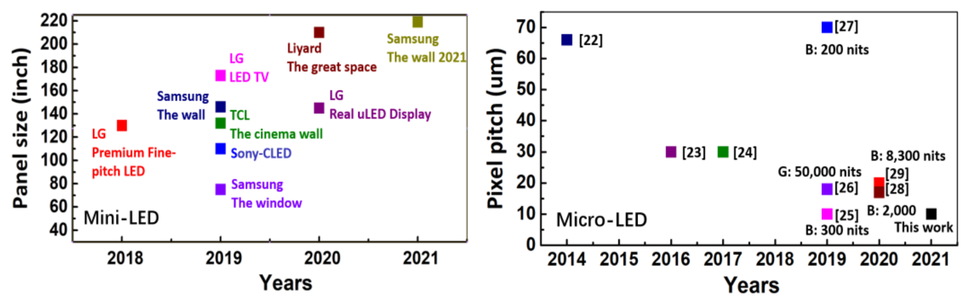
:1. Introduction
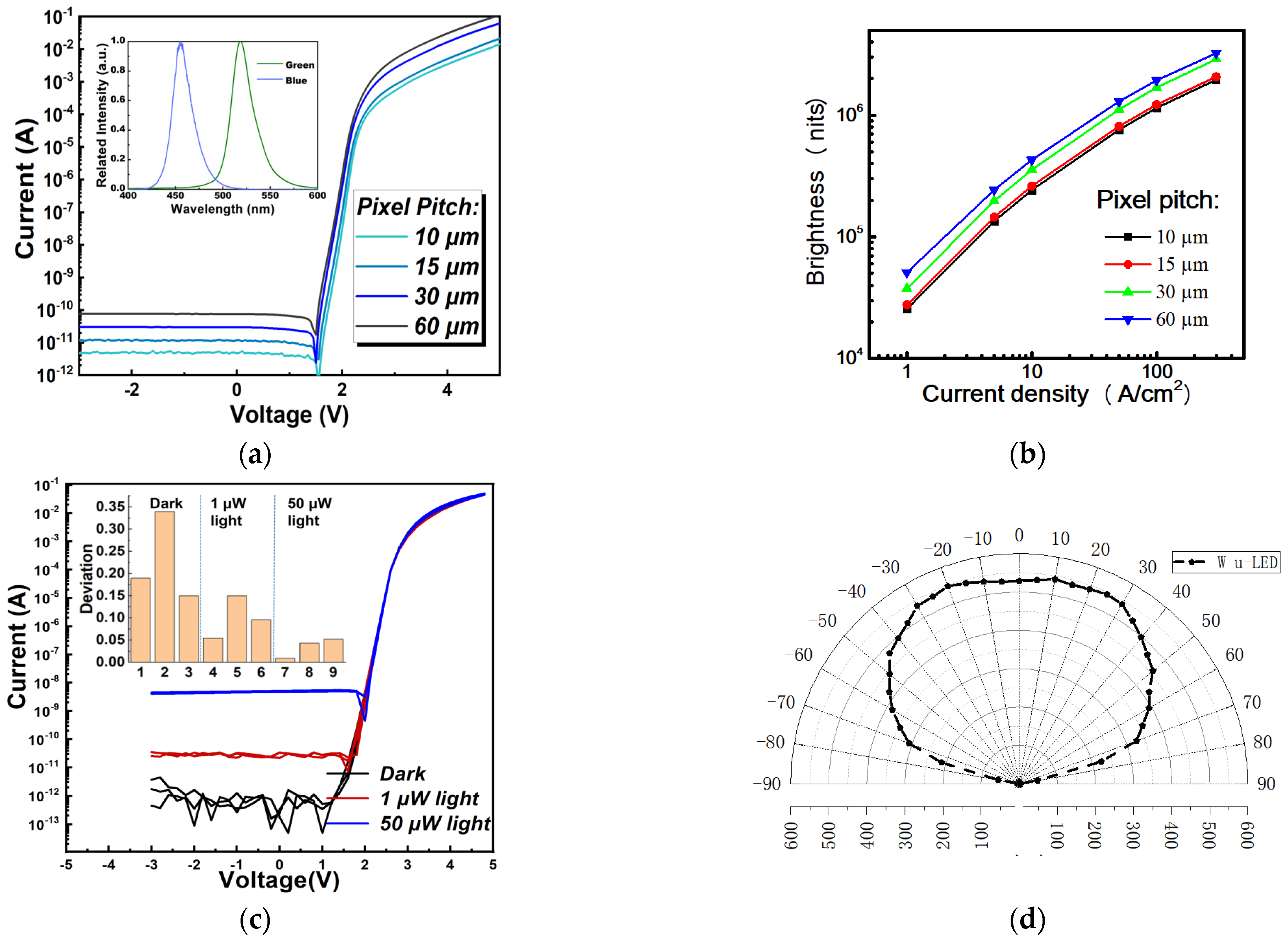
2. Fabrication and Characterization
3. ACR Principle
4. ACR: Experiment and Measurement
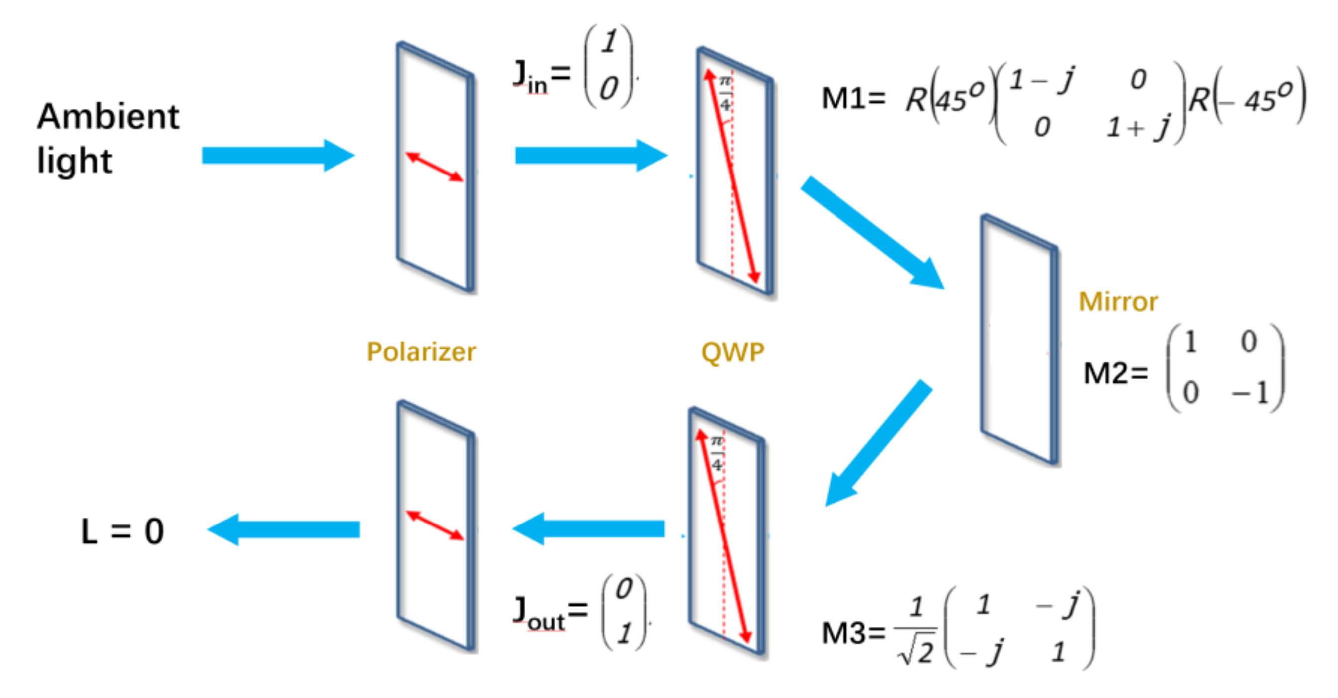
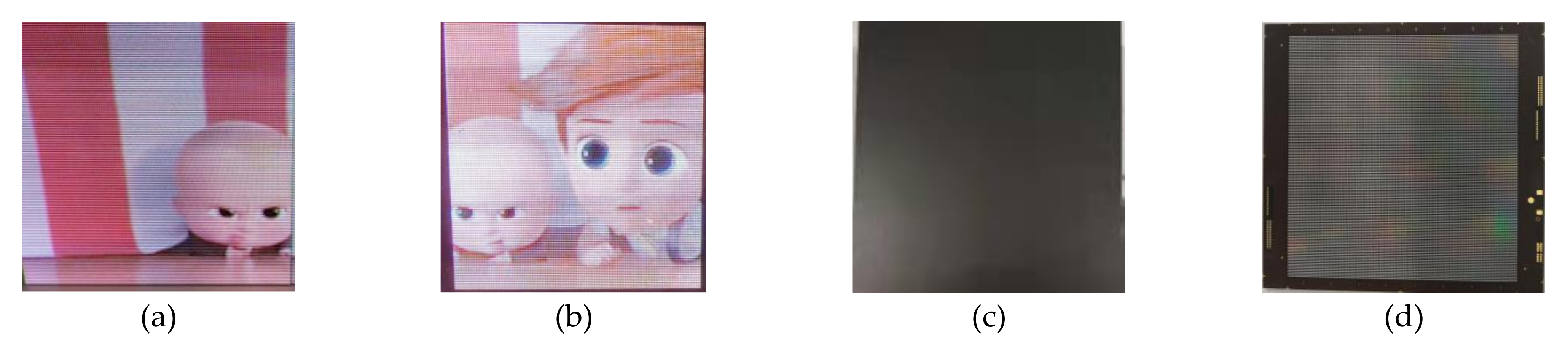
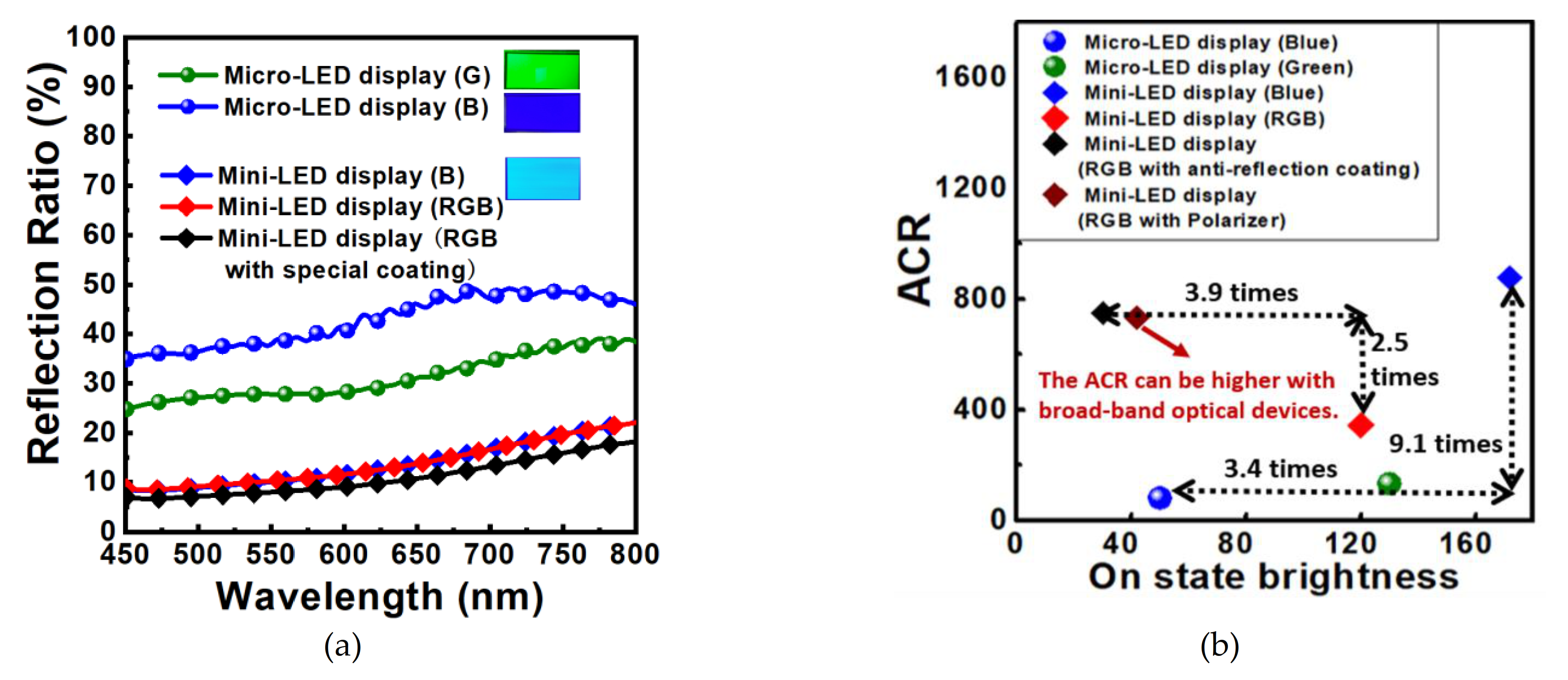
4.1. Optical Method
4.2. Antireflection Coating
4.3. Structure Optimization
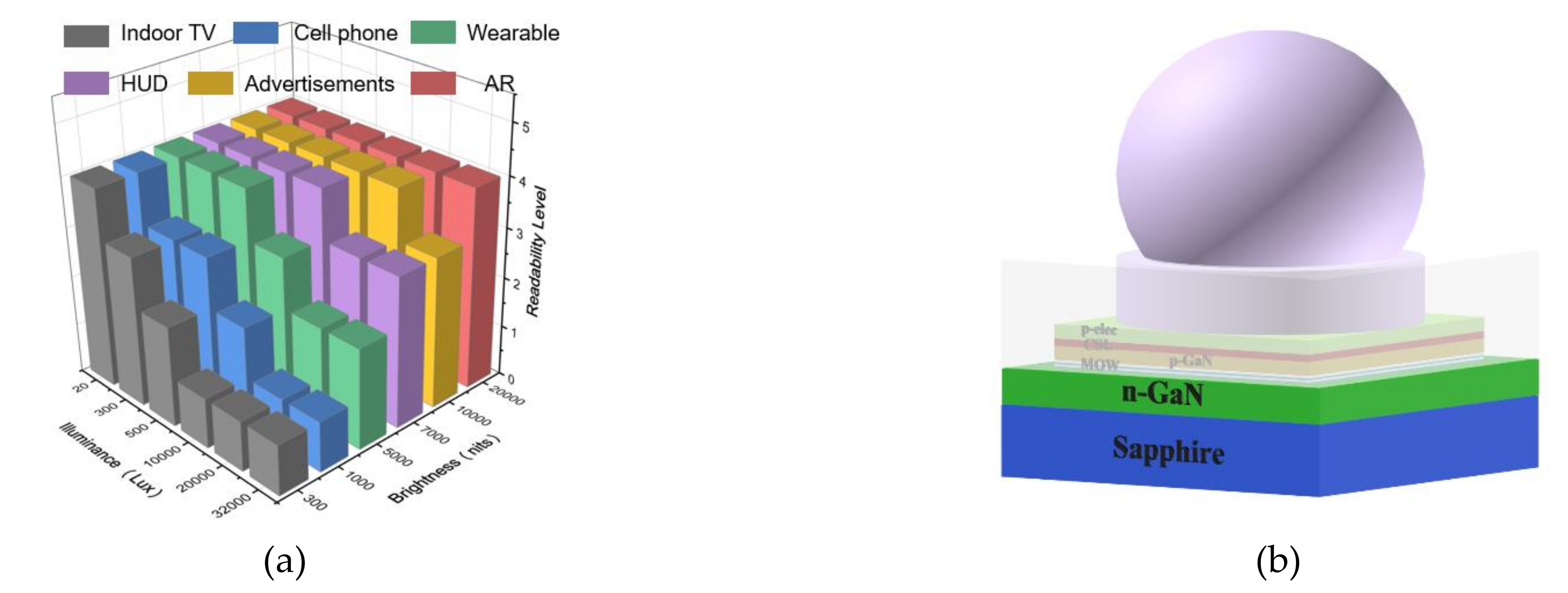
4.4. Discussions
5. Conclusions
Author Contributions
Funding
Institutional Review Board Statement
Informed Consent Statement
Acknowledgments
Conflicts of Interest
References
- Sabbar, A.; Madhusoodhanan, S.; Al-Kabi, S.; Dong, B.; Wang, J.; Atcitty, S.; Kaplar, R.; Ding, D.; Mantooth, A.; Yu, S.Q.; et al. High Temperature and Power Dependent Photoluminescence Analysis on Commercial Lighting and Display LED Materials for Future Power Electronic Modules. Sci. Rep. 2019, 9, 16758. [Google Scholar] [CrossRef] [PubMed]
- Wong, M.S.; Lee, C.; Myers, D.J.; Hwang, D.; Kearns, J.A.; Li, T.; Speck, J.S.; Nakamura, S.; Denbaars, S.P. Size-independent peak efficiency of III-nitride micro-light-emitting-diodes using chemical treatment and sidewall passivation. Appl. Phys. Express 2019, 12, 097004. [Google Scholar] [CrossRef]
- MacLure, D.M.; McKendry, J.J.D.; Herrnsdorf, J.; He, X.; Xie, E.; Gu, E.; Dawson, M.D. Size-Dependent Characterization of Deep UV Micro-Light-Emitting Diodes. In Proceedings of the 2020 IEEE Photonics Conference (IPC) 2020–2021, Vancouver, BC, Canada, 28 September–1 October 2020. [Google Scholar] [CrossRef]
- Wong, M.S.; Hwang, D.; Alhassan, A.I.; Lee, C.; Ley, R.; Nakamura, S.; DenBaars, S.P. High efficiency of III-nitride micro-light-emitting diodes by sidewall passivation using atomic layer deposition. Opt. Express 2018, 26, 21324. [Google Scholar] [CrossRef] [PubMed]
- Park, J.; Choi, J.H.; Kong, K.; Han, J.H.; Park, J.H.; Kim, N.; Lee, E.; Kim, D.; Kim, J.; Chung, D.; et al. Electrically driven mid-submicrometre pixelation of InGaN micro-light-emitting diode displays for augmented-reality glasses. Nat. Photonics 2021, 15, 449–455. [Google Scholar] [CrossRef]
- Cai, Y.; Zou, X.; Liu, C.; Lau, K.M. Voltage-Controlled GaN HEMT-LED Devices as Fast-Switching and Dimmable Light Emitters. IEEE Electron Device Lett. 2018, 39, 224–227. [Google Scholar] [CrossRef]
- Li, K.H.; Fu, W.Y.; Cheung, Y.F.; Wong, K.K.Y.; Wang, Y.; Lau, K.M.; Choi, H.W. Monolithically integrated InGaN/GaN light-emitting diodes, photodetectors, and waveguides on Si substrate. Optica 2018, 5, 564. [Google Scholar] [CrossRef]
- Kim, T. Optoelectronics with Applications. Science 2014, 211. [Google Scholar] [CrossRef] [Green Version]
- Li, K.H.; Fu, W.Y.; Choi, H.W. Chip-scale GaN integration. Prog. Quantum Electron. 2020, 70, 100247. [Google Scholar] [CrossRef]
- Lam, K.-T.; Lin, W.-H.; Shei, S.-C.; Lin, N.-M.; Chen, W.-S.; Chang, S.-J. White-Light Emission From GaN-Based TJ LEDs Coated With Red Phosphor. IEEE Electron Device Lett. 2016, 37, 1150–1153. [Google Scholar] [CrossRef]
- Choi, M.; Jang, B.; Lee, W.; Lee, S.; Kim, T.W.; Lee, H.-J.; Kim, J.-H.; Ahn, J.-H. Stretchable Active Matrix Inorganic Light-Emitting Diode Display Enabled by Overlay-Aligned Roll-Transfer Printing. Adv. Funct. Mater. 2017, 27, 1606005. [Google Scholar] [CrossRef]
- Lu, B.; Wang, Y.; Hyun, B.R.; Kuo, H.C.; Liu, Z. Color Difference and Thermal Stability of Flexible Transparent InGaN/GaN Multiple Quantum Wells Mini-LED Arrays. IEEE Electron Device Lett. 2020, 41, 1040–1043. [Google Scholar] [CrossRef]
- Qi, L.; Zhang, X.; Chong, W.C.; Li, P.; Tang, C.W.; Lau, K.M. Active matrix monolithic full-color LED micro-display. Proc. Int. Disp. Work. 2019, 2, 433–435. [Google Scholar] [CrossRef]
- Behrman, K.; Kymissis, I. Enhanced microLED efficiency via strategic pGaN contact geometries. Opt. Express 2021, 29, 14841–14852. [Google Scholar] [CrossRef]
- Soh, M.Y.; Ng, W.X.; Teo, T.H.; Selvaraj, S.L.; Peng, L.; Disney, D.; Zou, Q.; Yeo, K.S. Design and Characterization of Micro-LED Matrix Display with Heterogeneous Integration of GaN and BCD Technologies. IEEE Trans. Electron Devices 2019, 66, 4221–4227. [Google Scholar] [CrossRef]
- Tian, P.; Liu, X.; Yi, S.; Huang, Y.; Zhang, S.; Zhou, X.; Hu, L.; Zheng, L.; Liu, R. High-speed underwater optical wireless communication using a blue GaN-based micro-LED. Opt. Express 2017, 25, 1193–1201. [Google Scholar] [CrossRef]
- Zhang, K.; Liu, Y.; Kwok, H.S.; Liu, Z. Investigation of electrical properties and reliability of gan-based micro-leds. Nanomaterials 2020, 10, 689. [Google Scholar] [CrossRef] [Green Version]
- Chen, H.; Tan, G.; Wu, S.-T. Ambient contrast ratio of LCDs and OLED displays. Opt. Express 2017, 25, 33643. [Google Scholar] [CrossRef]
- Gou, F.; Hsiang, E.; Tan, G.; Lan, Y.; Tsai, C.; Wu, S.; Gou, F.; Hsiang, E.; Tan, G.; Lan, Y.; et al. High Efficiency Color-Converted Micro-LED Displays High Efficiency Color-Converted Micro-LED Displays. J. Soc. Inf. Disp. 2019, 27, 199–206. [Google Scholar] [CrossRef]
- Han, Y.; Meyer, S.; Dkhissi, Y.; Weber, K.; Pringle, J.M.; Bach, U.; Spiccia, L.; Cheng, Y.B. Degradation observations of encapsulated planar CH3NH3PbI3 perovskite solar cells at high temperatures and humidity. J. Mater. Chem. A 2015, 3, 8139–8147. [Google Scholar] [CrossRef]
- Gan, H.I.; Leds, P.F.; Lai, W.; Sheu, J.; Lin, A.J. High-Brightness InGaN–GaN Power Flip-Chip LEDs. J. Lightwave Technol. 2009, 27, 1985–1989. [Google Scholar]
- Liu, Z.J.; Chong, W.C.; Wong, K.M.; Lau, K.M. 360 PPI flip-chip mounted active matrix addressable light emitting diode on silicon (ledos) micro-displays. J. Disp. Technol. 2013, 9, 678–682. [Google Scholar] [CrossRef]
- Li, X.; Member, S.; Wu, L.; Liu, Z.; Hussain, B.; Member, S.; Chong, W.C.; Lau, K.M.; Yue, C.P. Design and Characterization of Active Matrix LED Microdisplays With Embedded Visible Light. J. Lightwave Technol. 2016, 34, 3449–3457. [Google Scholar] [CrossRef]
- Zhang, K.; Peng, D.; Lau, K.M.; Liu, Z. Fully-integrated active matrix programmable UV and blue micro-LED display system-on-panel (SoP). J. Soc. Inf. Disp. 2017, 25, 240–248. [Google Scholar] [CrossRef]
- Zhang, L. Wafer Scale Hybrid Monolithic Integration of Si-based IC and III-V Epilayers -a Mass Manufacturable Approach for Active Matrix micro-LED Displays. J. Soc. Inf. Disp. 2019, 26, 137–145. [Google Scholar] [CrossRef]
- Templier, F.; Bernard, J.; Caplet, S.; Bédoin, A.; Haas, H. Advanced solutions for high-performance GaN MicroLED displays. In Gallium Nitride Materials and Devices XIV; International Society for Optics and Photonics: Munich, Germany, 2019; Volume 61. [Google Scholar] [CrossRef]
- Um, J.G.; Jeong, D.Y.; Jung, Y.; Moon, J.K.; Jung, Y.H.; Kim, S.; Kim, S.H.; Lee, J.S.; Jang, J. Active-Matrix GaN µ-LED Display Using Oxide Thin-Film Transistor Backplane and Flip Chip LED Bonding. Adv. Electron. Mater. 2019, 5, 1800617. [Google Scholar] [CrossRef]
- Li, Y.L.; Liu, Y.T. MicroLED display: The next-generation display technology in Advances in Display Technologies. In Advances in Display Technologies X; International Society for Optics and Photonics: Bellingham, WA, USA, 2020; Volume 11304, p. 113040H. [Google Scholar]
- Qi, L.; Zhang, X.; Lau, K.M. 848 ppi high-brightness active-matrix micro-LED micro-display using GaN-on-Si epi-wafers towards mass production. Opt. Express 2021, 29, 27–50. [Google Scholar]
- Zhang, K.; Peng, D.; Lau, K.M.; Liu, Z. Investigation of Photon-Generated Leakage Current for High-Performance Active Matrix Micro-LED Displays. IEEE Trans. Electron Devices 2016, 63, 4832–4838. [Google Scholar] [CrossRef]
- Liu, Z.; Zhang, K.; Liu, Y.; Yan, S.; Kwok, H.S.; Deen, J.; Sun, X.; Blue, A.G.; Micro-leds, G. Fully Multi-Functional GaN-based Micro-LEDs for 2500 PPI Micro-displays, Temperature Sensing, Light Energy Harvesting, and Light Detection. In Proceedings of the 2018 IEEE International Electron Devices Meeting (IEDM), San Francisco, CA, USA, 1–5 December 2018; pp. 871–874. [Google Scholar]
- Gou, F.; Hsiang, E.-L.; Tan, G.; Chou, P.-T.; Li, Y.-L.; Lan, Y.-F.; Wu, S.-T. Angular color shift of micro-LED displays. Opt. Express 2019, 27, A746. [Google Scholar] [CrossRef]
- Vigier, M.; Pilloix, T.; Dupont, B.; Moritz, G. Very High Brightness, High Resolution CMOS Driving Circuit for Microdisplay in Augmented Reality. Midwest Symp. Circ. Syst. 2020, 2020, 876–879. [Google Scholar] [CrossRef]
- Liu, Y.; Zhang, K.; Hyun, B.R.; Kwok, H.S.; Liu, Z. High-Brightness InGaN/GaN Micro-LEDs with Secondary Peak Effect for Displays. IEEE Electron Device Lett. 2020, 41, 1380–1383. [Google Scholar] [CrossRef]
- Id, T.W.; Sher, C.; Lin, Y.; Lee, C.; Liang, S.; Lu, Y.; Chen, S.H.; Id, W.G.; Kuo, H.; Chen, Z. Mini-LED and Micro-LED: Promising Candidates for the Next Generation Display Technology. Appl. Sci. 2018, 8, 1557. [Google Scholar] [CrossRef] [Green Version]
- Tan, G.; Zhu, R.; Tsai, Y.; Lee, K. High ambient contrast ratio OLED and QLED without a circular polarizer. J. Phys. D: Appl. Phys. 2016, 49, 315101. [Google Scholar] [CrossRef]
- Isakov, K.; Kauppinen, C.; Franssila, S.; Lipsanen, H. Superhydrophobic Antireflection Coating on Glass Using Grass-like Alumina and Fluoropolymer. ACS Appl. Mater. Interfaces 2020, 12, 49957–49962. [Google Scholar] [CrossRef] [PubMed]
- Biwa, G.; Aoyagi, A.; Doi, M.; Tomoda, K.; Yasuda, A.; Kadota, H. Technologies for the Crystal LED display system. J. Soc. Inf. Disp. 2021, 29, 435–445. [Google Scholar] [CrossRef]
- Zhang, K.; Yan, S.; Liu, Y.; Han, T.; Cho, W.K.; Liu, Z.; Kwok, H.S. Improvement of ambient contrast of micro-LED devices with high reliability. SID Symp. Dig. Tech. Pap. 2019, 50, 133–136. [Google Scholar] [CrossRef]


| Display Panel (uW) | Micro-LED Panel (B) | Micro-LED Panel (G) | Mini-LED Panel (B) | Mini-LED Panel (RGB) | Mini-LED Panel (RGB with Coating) | Mini-LED Panel (RGB with Polarizer) | ||||||||||||
|---|---|---|---|---|---|---|---|---|---|---|---|---|---|---|---|---|---|---|
| Light Source | B | W | Y | B | W | Y | B | W | Y | B | W | Y | B | W | Y | B | W | Y |
| On state | 500 | 1300 | 1720 | 1200 | 302 | 419 | ||||||||||||
| Off state | 11.8 | 12 | 12.4 | 8.5 | 9.7 | 13.5 | 1.2 | 1.6 | 2.2 | 1.9 | 1.9 | 2.0 | 0.4 | 0.4 | 0.4 | 0.4 | 0.6 | 0.7 |
| ACR | 84 | 82 | 80 | 154 | 134 | 97 | 1182 | 877 | 581 | 343 | 344 | 315 | 725 | 750 | 719 | 986 | 733 | 576 |
Publisher’s Note: MDPI stays neutral with regard to jurisdictional claims in published maps and institutional affiliations. |
© 2021 by the authors. Licensee MDPI, Basel, Switzerland. This article is an open access article distributed under the terms and conditions of the Creative Commons Attribution (CC BY) license (https://creativecommons.org/licenses/by/4.0/).
Share and Cite
Zhang, K.; Han, T.; Cho, W.-K.; Kwok, H.-S.; Liu, Z. Investigation of Enhanced Ambient Contrast Ratio in Novel Micro/Mini-LED Displays. Nanomaterials 2021, 11, 3304. https://doi.org/10.3390/nano11123304
Zhang K, Han T, Cho W-K, Kwok H-S, Liu Z. Investigation of Enhanced Ambient Contrast Ratio in Novel Micro/Mini-LED Displays. Nanomaterials. 2021; 11(12):3304. https://doi.org/10.3390/nano11123304
Chicago/Turabian StyleZhang, Ke, Tingting Han, Wai-Keung Cho, Hoi-Sing Kwok, and Zhaojun Liu. 2021. "Investigation of Enhanced Ambient Contrast Ratio in Novel Micro/Mini-LED Displays" Nanomaterials 11, no. 12: 3304. https://doi.org/10.3390/nano11123304