1. Introduction
Recently,
n-type amorphous indium-gallium-zinc-oxide (a-IGZO) [
1] has been shown to be one of the most promising materials for amorphous oxide semiconductor (AOS)-based thin-film transistors (TFTs) for achieving a low-temperature process, high-resolution, and a low-power display [
2]. The AOS concept indicates that amorphous oxide is composed of heavy metal cations (HMC) with electronic configurations (
n − 1)d
10ns
0 (
n ≥ 4) [
3]. The high-mobility amorphous semiconductors can be achieved because largely spread spherical metal ns
0 orbitals constitute the lowest unoccupied states (conduction band minimum, CBM), and therefore they are expected to have a high electron mobility and a small electron effective mass in disordered amorphous structures [
3]. However, one of the instabilities results from acid-soluble Ga
2O
3 and ZnO contained in a-IGZO, which induces back channel damage when etching source/drain electrodes [
4]. The role of Ga
2O
3 in a-IGZO is to reduce oxygen vacancy (V
O) for improving the stability of devices [
4,
5,
6,
7,
8]. Replacing Ga and/or Zn in InO-based semiconductors, such as InTiO, InWO. etc., is an alternative way to suppress V
O for reducing instability [
4,
5,
6,
7,
8], which still maintains the electronic configurations of AOS. In our previous study for enhancing stability [
4], we doped a small amount of tungsten oxide (WO
3) into indium oxide (In
2O
3) film to replace gallium oxide (Ga
2O
3) from classic IGZO due to the high tungsten-oxide (W-O) bonding-dissociation energy (720 kJ/mol) compared to pure indium oxide (346 kJ/mol) [
9].
One of the most important features in amorphous semiconductors is electronic defects, and therefore the defects in either a-IGZO [
3,
10,
11,
12,
13,
14,
15] or other AOSs such as amorphous indium tin zinc oxide (a-ITZO) [
16] and amorphous tin oxide (a-SnO
x) [
17], etc., have been intensively investigated by theoretical DFT calculations [
18,
19,
20] and experiments. However widely varying process conditions of AOS mainly affect the density of states (DOS) at specific energy levels, corresponding with variations of different chemical species. Additional numerical analysis by Technology Computer Aided Design (TCAD) can be used to understand the physics and material properties in AOS TFTs by studying the effect of the bulk sub-gap density of states (DOS) on electrical characteristics [
10,
11,
12,
13,
14,
15,
16,
17]. Furthermore, for developing and exploring vast AOS materials, theoretical DFT calculations would be time-exhausting, and utilizing TCAD numerical analysis together with simple material analysis could an alternative and prompt solution to AOS devices.
Furthermore, by using the unique feature of junctionless transistors (JLTs) [
21] in CMOS technology, critical control of the dopant profile of source/drain can be avoided to resolve short channel effects (SCEs), such as the instability in threshold voltage (
VTH) as the channel length (L) scales down to a nanometer scale scheme. Additionally, for the gate insulator (GI), certain high-κ materials [
22], such as aluminum oxide (Al
2O
3) and hafnium oxide (HfO
2), have been deposited by atomic layer deposition (ALD) [
23] with several advantages such as atomic-scaled thickness control, high film density, and superior step coverage and uniformity. Therefore, our previous study demonstrated that the integration of a HfO
2 GI and ultra-thin amorphous indium tungsten oxide (a-IWO) junctionless TFT can be achieved with promising electrical characteristics, such as high field-effect mobility (
μFE), near ideal subthreshold swing (
S.S.) (63 mV/dec), and large ON/OFF current ratios (I
ON/I
OFF) (1.5 × 10
8) [
24]. In this work, we investigate experimentally the electrical properties of nanosheet (NS) junctionless a-IWO TFT dependent on different oxygen flows during a-IWO deposition, and then deduce numerically the correlation among the chemical species, materials properties, DOS, and band diagrams by TCAD [
25].
3. Simulation Methodology
The chemical properties of the a-IWO films dependent on the different oxygen ratios, which were analyzed by X-ray photoelectron spectroscopy (XPS), Instrumentation Center, Taichung City, Taiwan, which can be used to determine qualitatively the bulk DOS of a-IWO for assuring AOS formed with spread spherical metal ns
0 orbitals in conduction band minimum (CBM) with high electron mobility. To understand the physical mechanisms and materials properties of the a-IWO TFT, TCAD was used for numerical analysis. Measured physical quantities such as layer thicknesses, bandgap (
Eg), and dielectric permittivity (
ε) of a-IWO and HfO
2 were input as the simulation parameters to accurately analyze the physical mechanisms. The bandgaps (
Eg) of a-IWO and HfO
2 were 3.05 eV and 5.70 eV, respectively. The electron affinity of a-IWO was estimated as 4.30 eV by the linear relation (1). Schottky barrier work function (
ΦSD) at S/D and Gate electrode’s work function (
ΦG) were 4.67 eV and 4.80 eV, respectively. The carrier concentration
n and
n-type doping concentration
Nd of a-IWO determined by Hall effect measurement as inputs for more accurate simulation. We initially assumed
Nd was 8 × 10
18 cm
−3 for a 3% oxygen ratio of a-IWO film; then, the other corresponding
Nd could be deduced for other oxygen ratios of a-IWO.
Based on the intensively investigated electronic defects in AOSs [
3,
18,
19], especially for IGZO structures, other AOS TFTs, such as a-SnOx, a-ITZO, etc., have also been numerically analyzed by characterizing the DOS [
16,
17]. Therefore, in this study, the adopted physical models and materials properties of a-IWO TFT were fundamentally inherited from a-IGZO publications and then corrected to some extent by materials measurements and TCAD calibration or assumptions [
10,
11,
12,
13,
14,
15,
16,
17] from measured transfer characteristics. The physical models contain Maxwell–Boltzmann statistics, the drift-diffusion (DD) model, Poisson’s equation, and carrier continuity equations with Shockley–Read–Hall (SRH) recombination. The Bohm quantum potential (BQP) model [
26] was enabled for obtaining accurate space charge density in an ultra-thin semiconductor. A Schottky tunneling model was used at the S/D metal–semiconductor (MS) interface [
27]. The electron mobility model was used from a-IGZO dependent on electron concentration
n and lattice temperature
TL in Equations (2) and (3) [
28].
where
μn0 is the intrinsic electron mobility; in this study,
μn0 was based on the experimentally extracted field-effect mobility (
μFE).
n is the electron concentration, which can refer to the Hall measurement. Default critical electron concentration
ncrit was 1 × 10
20 cm
−3. In this study, the temperature coefficient of electron mobility
γ was determined by setting the intrinsic temperature coefficient
γ0, lattice temperature
TL and temperature coefficient
Tγ as −0.36, 300 K and 178.4 K, respectively [
28].
As for one of the basic semiconductor equations is Poisson’s equation relating the electrostatic potential (
φ) to the space charge density (
ρ) and is given by
where
ε is the local permittivity of a-IWO, and HfO
2 was set to 10 and 18, respectively.
q is the elementary charge,
pfree and
nfree are the free hole and electron density, respectively, and the ionized densities of acceptor-like and donor-like trap (
nT and
pT, respectively) are given in Equations (5) and (6), which are integrated from valance band edge
EV to conduction band edge
EC.
The densities of ionized traps relate the occupation probability
f(
E) of a trap level at energy
E in Equations (7) and (8) for the acceptor and donor traps, respectively, which are dependent on the intrinsic carrier concentration
ni, intrinsic Fermi level
Ei, lattice temperature
TL, capture cross sections (
σE and
σH), and the thermal velocity (
υn and
υp) for the electron and hole. The occupation probability
f(
E) describes that traps are either filled with electrons or empty; then, it has a value in the range of 0 to 1, and consequently the Fermi energy position can be determined when
f(
E) = 0.5. The occupation probability
f(
E) and thermal velocity
υn and
υp for the electron and hole in Equations (9) and (10) can be determined by assuming the Richardson coefficients (
An,
Ap) of 41 A·cm
−2·k
−2 [
29], capture cross sections
σE and
σH of 1 × 10
12 cm
2 [
30], and conduction/valance band effective density of states (
NC =
NV) of 2.0 × 10
18 cm
−3, initially estimated from the carrier concentration of Hall measurements.
Equation (11) shows that the density of state (DOS)
g(
E) of AOS is composed of an acceptor-like trap
gA(
E) and a donor-like trap
gD(
E), with a combination of exponential tail and Gaussian distributions. In this study, we assumed the chemical properties between a-IWO and a-IGZO were similar, and then the schematic DOS of a-IGZO represented in
Figure 1b could be used as a starting point to simulate the a-IWO TFT. In order to understand that each DOS distribution stands for the corresponding chemical species in AOS film, in this study we defined different mid-gap DOS distributions as control variables for examining the effects on electrical characteristics in later sections. Through the analysis of the O 1s by XPS [
31], it provides a mean to investigate the oxygen-related states in AOS, which can be related to some numerical DOS parameters. Therefore, the bulk and interfacial DOS can be extracted depending on the oxygen ratio during a-IWO deposition. As a result, the proposed physical models and material properties of a-IWO TFT can be validated by TCAD.
First, the DOS of the metal-ions s-band [
10,
12,
23] can be modeled by conduction band tail DOS
gTA(
E) in Equation (12), and
Figure 1b describes the conduction band edge intercept densities
NTA and its decay energy
WTA. NTA is associated with lowering the electron concentration [
3]. In this simulation, we assumed
gTA(
E) was fixed by setting
NTA at 5.0 × 10
19 cm
−3·eV
−1 and
WTA at 0.01 eV [
32], because by controlling
Nd and
NC, we could observe the change of electron concentration dependent on the oxygen ratio of a-IWO in later sections. On the other hand, the deep DOS of the oxygen
p-band [
23] can be represented by valance band tail DOS
gTD(
E) in Equation (13) and
Figure 1b relating to valence band edge intercept densities
NTD and its decay energy
WTD. Since the transfer I
D–V
G curve was found not affected by deep defect
NTD [
32], we assumed
gTD(
E) was fixed by setting
NTD of 8.0 × 10
20 cm
−3·eV
−1 and
WTD of 0.12 eV for various oxygen ratios of a-IWO [
11].
The DOS of oxygen vacancy (V
O) can be modeled by the Gaussian donor state
gGD(
E) in Equation (14) and
Figure 1b [
13], which is dependent on total density
NGD, decay energy
WGD, and peak energy distribution
EGD positioned near
EC by the effect of Madelung potential [
3]. Since the amount of V
O can be analyzed by XPS for different oxygen ratios of a-IWO, we initially assumed an
NGD of 5.0 × 10
16 cm
−3·eV
−1 with a fixed
WGD of 0.05 eV and an
EGD of 2.95 eV for a 3% oxygen ratio of a-IWO TFT [
13]. Then, the I
D–V
G curves were simulated, affected by different
NGD values, as shown in a later section.
Other DOS of chemical species relating to hydroxyl (–OH) groups [
3], interstitial oxygen (O
i) [
33], or metal vacancy [
18] in
a-IGZO can be modeled by Gaussian acceptor state
gGA(
E) in Equation (15) and
Figure 1b, which is dependent on total density
NGA, decay energy
WGA, and peak energy distribution
EGA. To qualitatively analyze the effect of the Gaussian acceptor state in different oxygen ratios of bulk a-IWO, we initially assumed an
NGA of 1.0 × 10
16 cm
−3·eV
−1 with a fixed
WGA of 0.04 eV and
EGA of 0.30 eV [
11]. The effect of the
NGA value at the front interface between a-IWO and HfO
2 on transfer characteristics is discussed as well.
The positive gate-bias stress (PGBS) condition causes a positive
VTH shift (∆
VTH), explained by some possible mechanisms such as electron trapping [
3] or Joule heating with a hot carrier effect [
34], etc. However, in our study, there was no hot carrier effect in the PGBS condition (V
D = vs. = 0 V, V
G = +2 MV/cm) at room temperature, so we should consider electron trapping after PGBS. Furthermore, it has been reported that a positive
VTH shift (∆
VTH) increases with higher oxygen ratio of AOS TFTs after PGBS [
35], which could be ascribed to the greater number of interface traps due to the stronger ion bombardment in the sputtering process [
35]. As a result, the geometrical location of interface traps was estimated as the characteristic penetration depth (
d), which implies charge trapping takes place near the interface between GI and a-IGZO [
35]. Moreover, the created oxygen interstitials (O
i) in the octahedral configuration [
18,
19] after PGBS, which have been investigated by the first-principles calculation based on density functional theory (DFT). When a large positive V
G is applied, the Fermi level (
EF) increases greatly so that the neutral O
i0 states around
EF are occupied by electrons and thus form the negatively charged O
i2− as chemical reaction formula O
i0 + 2e
− ν O
i2−. During PGBS, a stronger defect-lattice electrostatic interaction occurs, and the energy level of a charged state can be lowered below that of the neutral state due to the structural relaxation invoked [
29]; such behavior also has been found in amorphous silicon, known as “negative-U” behavior [
33,
36]. In the oxygen-rich a-IGZO channel, many weakly bonded oxygen can be express as –M
I⋯O
i0⋯M
II–, where M
I and M
II denote metal cations, “–” strong chemical bonds and “⋯” weak chemical bonds [
35]. Therefore, it is inferred that weakly bonded oxygen ions are easily ionized under PGBS to form oxygen interstitial (O
i) defects due to the low defect formation energy
Ef [
20,
36]. The concentration of a native defect in a solid is determined by its formation energy
Ef through Equation (16) [
20].
where
Nsites is the number of sites per unit volume (including different configurations) the defect can be incorporated on, the defect formation energy
Ef is dependent on not only the Fermi level
EF but also the chemical potential of the species,
kB is the Boltzmann constant, and
T is the temperature. Through the DFT calculations, the low defect formation energy of O
i in ZnO was found at a high Fermi level (
EF) [
14,
20]; therefore, one can roughly estimate the possible distribution of O
i by observing a high Fermi level (
EF) in AOS TFTs simulation in a later section.
4. Results and Discussion
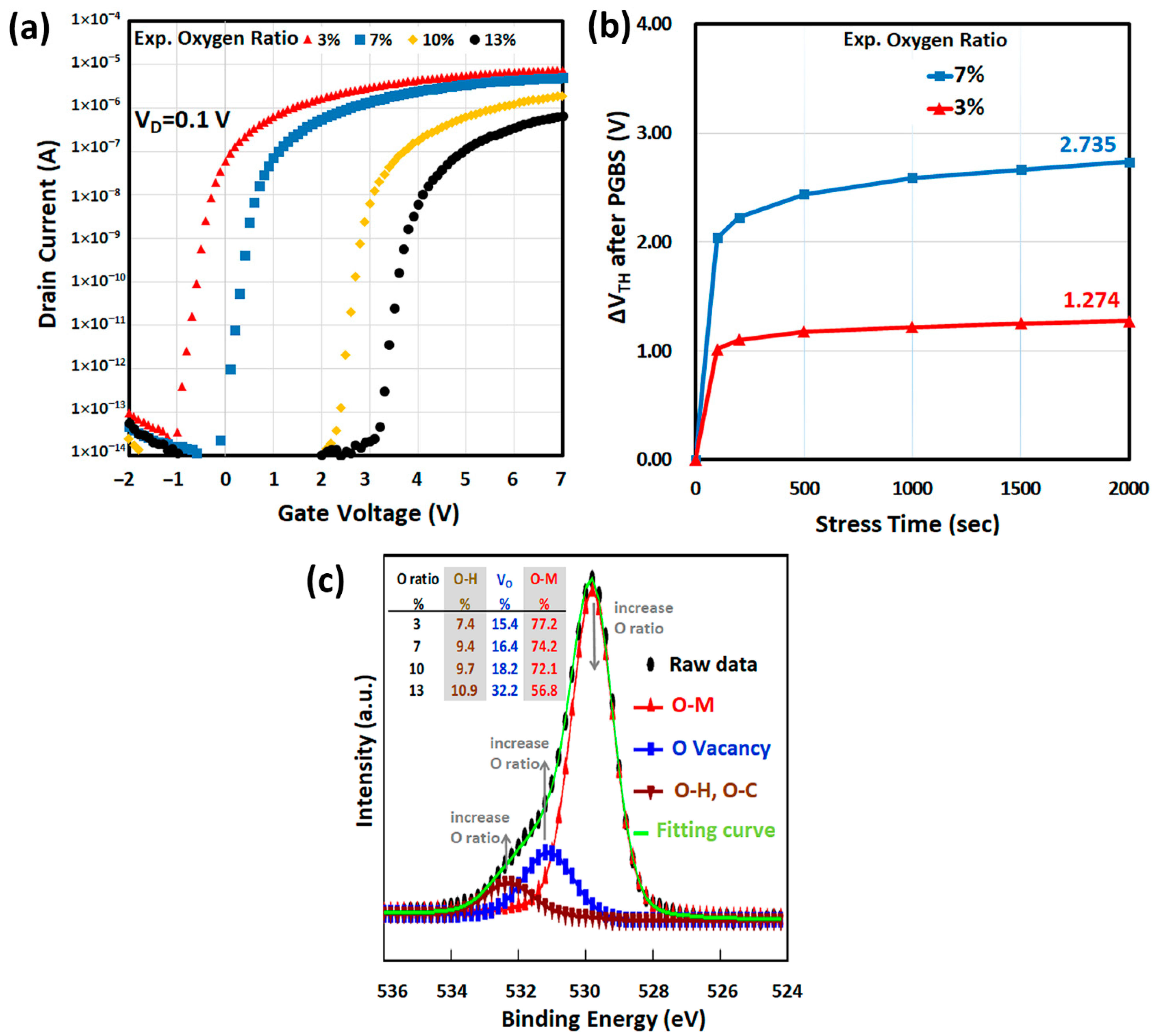
The measured transfer characteristics of a-IWO TFT and the extracted electrical parameters with different oxygen ratios are shown in
Figure 2a and
Table 1, respectively. When the oxygen ratio increased, the on-state current (
ION) of the device decreased, the threshold voltage (
VTH) increased, the subthreshold swing (
S.S.) degraded, and the field-effect mobility (
μFE) declined correspondingly. The extracted
μFE dependent on oxygen ratios of a-IWO, in
Table 1, were input as the simulation parameters for more accurate material properties. As for the affected transfer characteristics after the PGBS condition (V
D = vs. = 0 V, V
G = +2 MV/cm) for a certain duration time (2000 s) at room temperature in atmosphere, the stress time dependence of threshold voltage shift (∆
VTH) was extracted, as shown in
Figure 2b. Because the transfer characteristics severely degraded with 10% and 13% oxygen ratios after PGBS, the ∆
VTH with only 3% and 7% oxygen ratios are shown; it is noted that the reliability can be improved with low oxygen ratio of a-IWO film.
To verify the mechanisms of positive ∆
VTH with the increasing oxygen ratio, the chemical-bonding states of the a-IWO films were observed using XPS. Because the 4 nm a-IWO active semiconductor was thinner than the 10 nm XPS penetration depth, the prepared sample was 4 nm thick a-IWO film deposited on silicon substrate for analyzing chemical properties of bulk film. In this study, for qualitative numerical analysis, the compositions ratio from XPS O 1s peak could be referenced to deduce the amounts of different density of states (DOS) parameters for AOS simulation.
Figure 2c shows the normalized O 1s spectra with increasing oxygen ratios, deconvoluted into three peaks at 529.6, 530.9, and 532.1 eV, respectively. The lowest peak represented the oxygen–metal (O–M) bonding for lattice oxygen (O
L). The medium peak represented the oxygen vacancy (V
O), such as the dangling bond or weak bond in oxygen deficient lattice. The highest peak represented the –OH groups, which related to moisture in thin films. When the oxygen ratio increased, the ratios of the area under the spectrum of V
O increased from 15.4% to 32.2%, shown in the inset of
Figure 2c, where the –OH group also increased from 7.4% to 10.9%.
Apart from XPS O 1s analysis, the stability of a-IWO film can be investigated by XPS W 4f analysis [
37]. In the atmosphere, pure tungsten oxide
W6+O3 is more stable than
W4+O2, as shown in the following chemical reaction:
[
37]. The XPS W 4f spectrum can be deconvoluted into two species (W
6+ and W
4+), and therefore the W
6+ ratio can be regarded as a stability factor. In this study, through XPS W 4f material analysis, the extracted W
6+ ratios were 83.0, 76.3, 74.9, and 71.0% for 3%, 7%, 10%, and 13% oxygen ratios of a-IWO, respectively. As a result, it could be referred that excess oxygen could produce the unstable
W4+, resulting in an instability, which is consistent with the PGBS results in
Figure 2b.
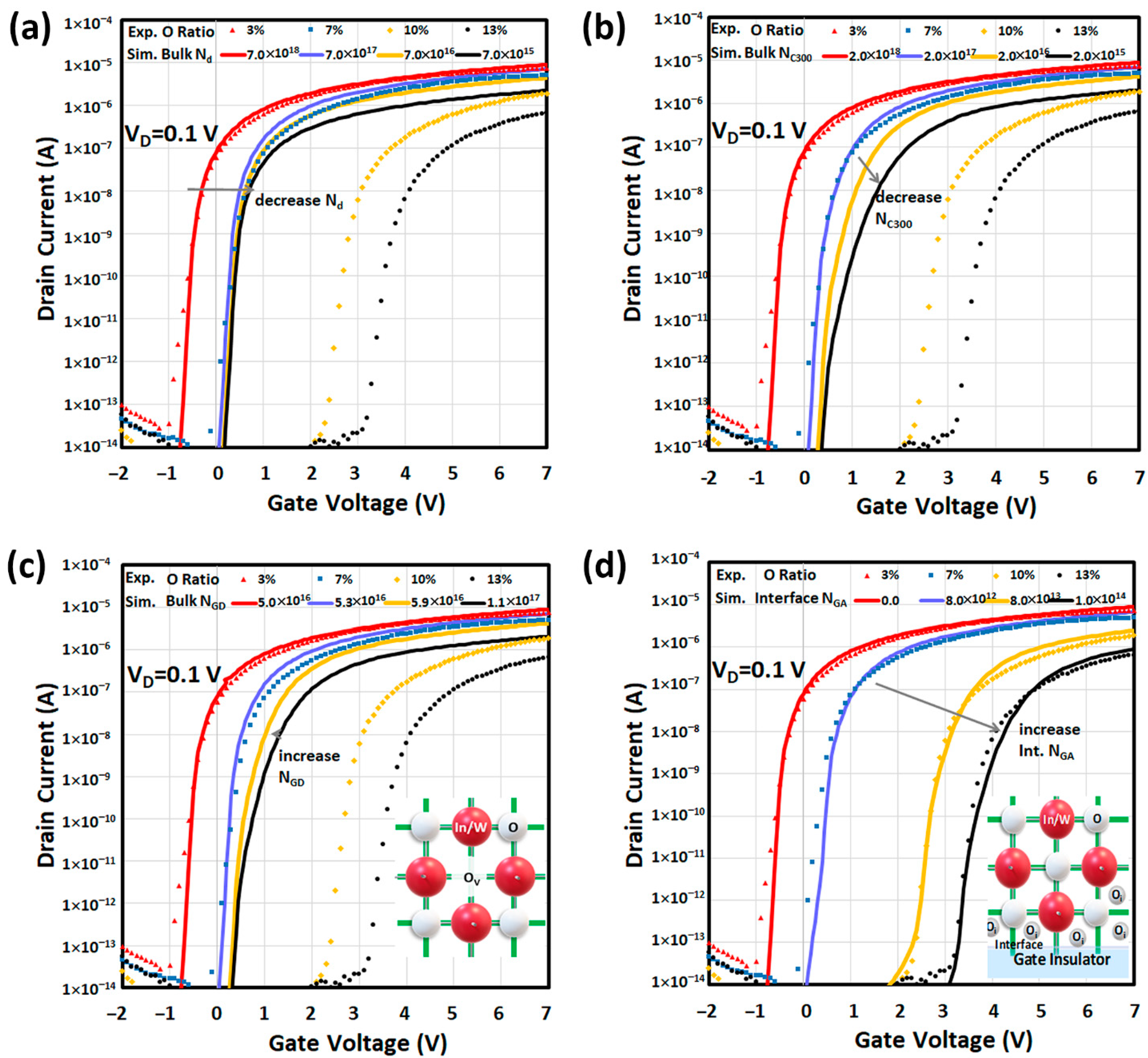
4.1. Effect of Dopant Concentration
According to the Poisson’s equation, changing the dopant concentration
Nd in device simulation can change the carrier concentration. As a result, the variation of carrier concentration of a-IWO for different oxygen ratios, observed by Hall measurement, can relate to the modulation of dopant concentration
Nd. Hence, we simulated how the linear I
D–V
G curves affected by
Nd of a-IWO varied from 7.0 × 10
18 to 7.0 × 10
15 cm
−3 in
Figure 3a. Although it showed a good fitting on electrical characteristics between measurements and simulations for a 3% oxygen ratio of a-IWO, it is noted that the simulated
VTH shift still could not approach the measurements for 10% and 13% oxygen ratios even with less
Nd. For the next analysis of conduction band density of states
NC in a-IWO, we controlled
Nd to be 7.0 × 10
18, 1.0 × 10
18, 5.0 × 10
15, and 5.0 × 10
15 cm
−3 for 3%, 7%, 10%, and 13% oxygen ratios of a-IWO respectively.
4.2. Effect of Conduction Band Density
Although the carrier concentration can be determined by Hall analysis, in device simulation, electron concentration is also affected by conduction band density
NC, according to the related Equations (5), (7), and (9). However,
NC cannot be directly determined by Hall measurement; therefore,
NC values can be numerically deduced for different oxygen ratios of a-IWO. In this section, we simulated how the linear I
D–V
G curves affected by
NC of a-IWO varied from 2.0 × 10
18 to 2.0 × 10
15 cm
−3 in
Figure 3b. It was found that the decreased
NC could reduce the simulated S.S. and I
ON with a more positive
VTH shift (∆
VTH), and although it was similar to the observed phenomena shown in
Figure 2a, nevertheless modulating
NC still could not match with the measurements. In the next section, for analyzing the electronic defect, we controlled
NC to be 2.0 × 10
18, 1.0 × 10
18, 3.0 × 10
16, and 8.0 × 10
15 cm
−3 for 3%, 7%, 10%, and 13% oxygen ratios of a-IWO, respectively. In this numerical approach, the physical properties such as band parameters
Nd,
NC, or traps, etc., inside a-IWO film can be inferred by fitting with the measured transfer characteristics with different oxygen ratios of a-IWO TFT.
4.3. Effect of Gaussian Donor Trap in Bulk a-IWO Film
According to the amount of V
O by XPS in
Figure 2c, the density of a Gaussian donor trap
NGD can be correlated and assumed to be 5.0 × 10
16, 5.3 × 10
16, 5.9 × 10
16, and 1.1 × 10
17 cm
−3·eV
−1 for 3%, 7%, 10%, and 13% oxygen ratios of a-IWO, respectively. The simulated linear I
D–V
G curves affected by the amount of
NGD are shown in
Figure 3c. It was found that more donor traps are ionized as the amount of
pT increased, which was associated with electron generation shown in Equations (6), (8), and Poisson’s equation, so the simulated
VTH changed in a negative shift with increasing
NGD [
10]. Hereafter, we elucidated that V
O cannot result in a positive
VTH shift (∆
VTH) with increasing oxygen flow during a-IWO deposition. A simple schematic of V
O is shown in the inset of
Figure 3c. In the next section, for analyzing a Gaussian acceptor trap, we adopted the aforementioned
NGD values for different oxygen ratios of a-IWO to observe the simulated linear I
D–V
G curves affected by the amount of
NGA inside bulk a-IWO.
4.4. Effect of Gaussian Acceptor Trap in Bulk a-IWO Film
In the previous XPS O 1s spectra in which the peak intensity at 532.1 eV that could be strictly regarded as the summation from –OH, O
i, and metal vacancy (V
M) species, according to the inset table of
Figure 2c, its amounts were less than 11% in the total amount of oxygen-related species even with a 13% oxygen ratio of a-IWO. Hence, in this section, we simply denoted it as –OH species by setting the density of the Gaussian acceptor trap
NGA value in bulk a-IWO film, calculated by observing the amount of –OH and V
O species at 532.1 and 530.9 eV in
Figure 2c, respectively. It was noted that the ratio of V
O to –OH was found between 2 and 3. On the other hand, according to the
Section 4.3, the density of V
O was set between 5.0 × 10
16 and 1.1 × 10
17 cm
−3·eV
−1, and therefore the density of –OH species could be calculated from 2.5 × 10
16 to 3.7 × 10
16 cm
−3·eV
−1 with the increasing oxygen ratio. After modulating the range of
NGA, it was found that the simulated I
D–V
G curves were unaffected, as in
Figure 3c [
11]. In the next section, we adopted the aforementioned bulk
NGA values for different oxygen ratios of a-IWO to observe the simulated linear I
D–V
G curves affected by the density of interfacial Gaussian acceptor trap
NGA. Furthermore, referring to the Poisson’s equation and relations (5), (7), we estimated the acceptor traps not to be ionized as the amount of
nT, which could result from Fermi level position, so the analysis of occupation probability
f(
E) of a trap level at energy
E and Fermi level are presented as well in
Section 4.6.
4.5. Effect of Gaussian Acceptor Trap at Interface
Because a passivation layer was deposited at the back interface [
8], then we assumed that the back interface does not have an interface trap. Furthermore, we assumed the Gaussian acceptor trap to be at the front interface between a-IWO and HfO
2 as the possible electron recombination, then the simulated linear I
D–V
G curves affected by interface
NGA shown in
Figure 3d. To match with the measured I
D–V
G curves, the extracted interface
NGA were 0, 8.0 × 10
12, 8.0 × 10
13, and 1.0 × 10
14 cm
−2 eV
−1 for 3%, 7%, 10%, and 13% oxygen ratios of a-IWO, respectively. Consequently, the lower the oxygen ratio of IWO, the lower the interface Gaussian acceptor trap at the front interface was elucidated by simulation, mainly contributing the remarkable experimental electrical characteristics of the a-IWO nanosheet TFT, such as near ideal
S.S., small
VTH, and enhanced
ION [
24]. Here the possible species at the front interface could be oxygen interstitial (O
i) [
33], and a simple schematic of O
i is shown in the inset of
Figure 3d.
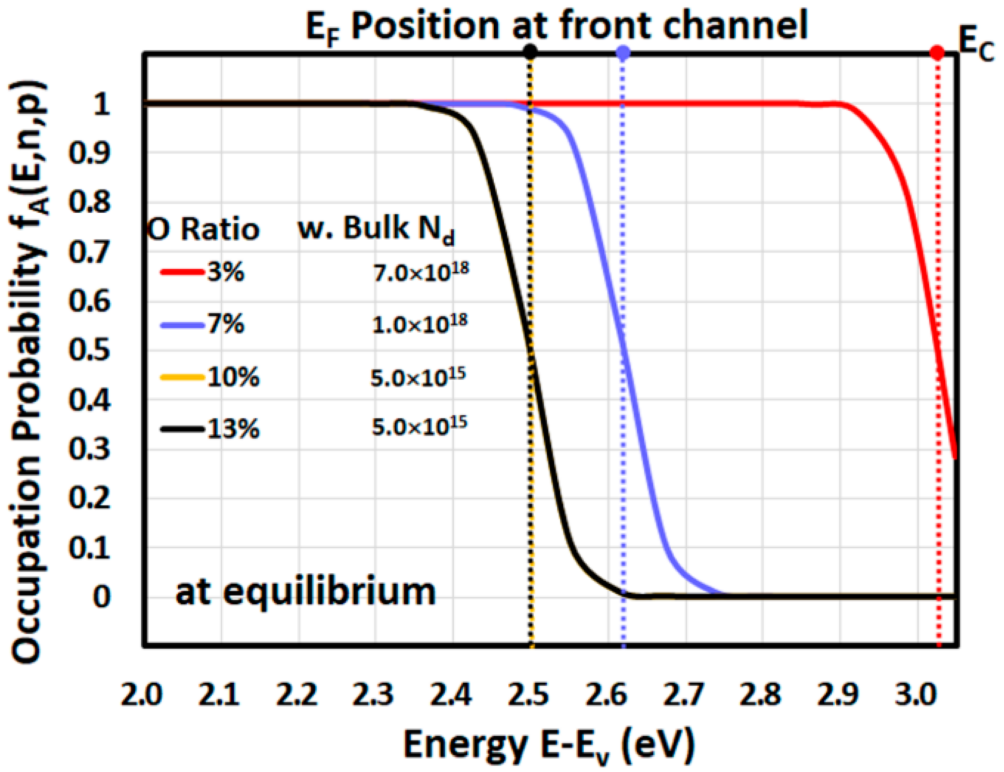
4.6. Analysis of 1D Fermi Level
To better understand the physics of a-IWO TFT for each oxygen ratio, the analysis of occupation probability
f(
E) of either electrons or acceptor traps under equilibrium condition (V
G = V
D = vs. = 0V) is essential to observe Fermi levels in
Figure 4. The different Fermi level positions near front channel of a-IWO TFT can be determined when
f(
E) = 0.5 and were dominated mainly by the bulk dopant concentration
Nd.
Figure 4 indicates the Fermi level position near
EC of only 0.025 eV in a 3% oxygen ratio of a-IWO, representing heavily doped
n-type material, whereas the observed Fermi level positions were away from
EC for higher oxygen ratios of a-IWO, meaning lightly doped
n-type material formed consequently. More specifically, the physical mechanisms in a-IWO TFT can be correlated with different DOS from chemical species by analyzing each one-dimensional (1D) energy band diagram, including the Fermi level for different oxygen ratios and bias conditions, and then the 1D and two-dimensional (2D) electron concentration distributions are discussed in later sections.
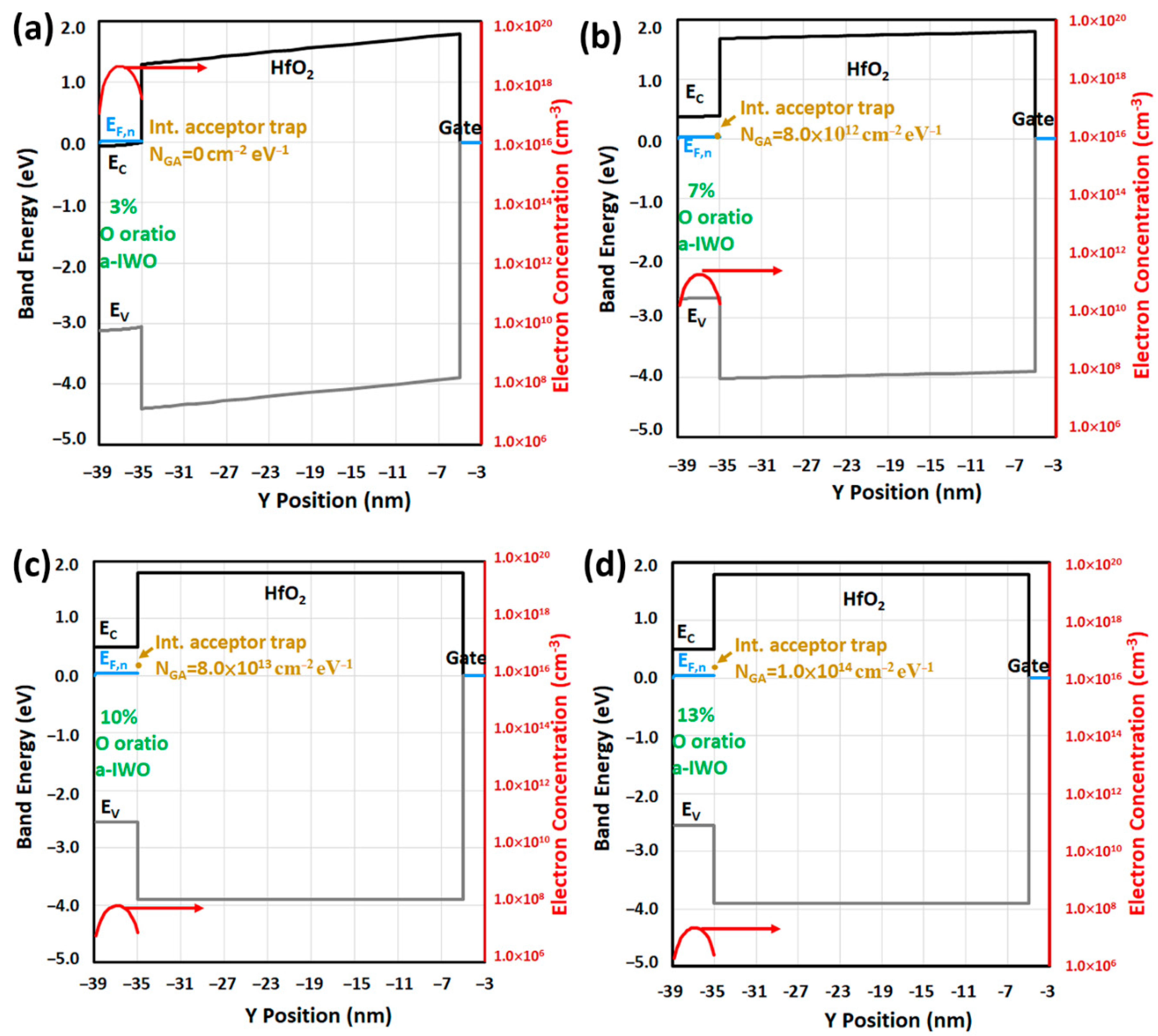
4.7. Analysis of Band Diagram
At equilibrium, the 1D band diagrams from back channel to bottom gate for different oxygen ratios of a-IWO TFT are shown in
Figure 5a–d. The 1D electron Fermi level
EF,
n and its corresponding electron concentration distribution inside a-IWO were plotted as well, which can be attributed to the previous effects including bulk dopant concentration
Nd, conduction band density
NC, and different chemical DOS distributions.
Figure 5a shows the presence of a slight accumulation mode for higher electron concentrations in a 3% oxygen ratio of a-IWO, whereas the depletion modes with flat-bands for higher oxygen ratios of a-IWO depicted in
Figure 5b–d, resulted in the reduced electron concentrations. The different interface densities of Gaussian acceptor trap
NGA at the front channel are introduced in
Figure 5b–d; it is noted that the
EF,n at front interface were below the trap energy
EGA, meaning interface acceptor traps were not ionized as easily as
nT at equilibrium. As a result, at equilibrium, the interface Gaussian acceptor trap was not the main reason for reducing electron concentration inside a-IWO TFT.
Further increasing the gate voltage to the on-state (V
G = 7V, V
D = 0.1V, vs. = 0V), the focus of 1D band diagrams is on the front channel of a-IWO TFT, depicted in
Figure 6a–d for different oxygen ratios. This indicates that the conduction band edges
EC near the front interface were bent by V
G, and hence the sharp peak electron concentration shifted to the front channel. The various band diagrams represent different degrees of the accumulation mode of a-IWO TFT with different oxygen ratio processes, which were associated with the previous effects including bulk dopant concentration
Nd, conduction band density of states
NC, and interface Gaussian acceptor trap density
NGA. The interface Gaussian acceptor trap
gGA(E) at the front channel are introduced in
Figure 6b–d; it was found that the
EF,n near the front interface were high and above the interface trap energy
EGA, meaning interface acceptor traps were ionized as
nT, especially in high oxygen ratios of a-IWO, which are associated with electron recombination, with a positive
VTH shift (∆
VTH) observed as a consequence.
4.8. Analysis of 2D Distribution of Oxygen Interstitials (Oi) Formed by Electric Field
In the on-state (V
G = 7V, V
D = 0.1V, vs. = 0V), large conduction band bending occurs, as observed in
Figure 6a–d, resulting in a large electric field (>2 MV/cm) at the front channel, which is like the condition of PGBS. In the
Section 4.5, the positive ∆
VTH was analyzed by the interface Gaussian acceptor trap
gGA(
E), which could be ascribed to created oxygen interstitials (O
i) either under a large electric field or a strong ion bombardment in sputtering process [
35]. Furthermore, through the Equation (16) by DFT, we assumed the formation of O
i mainly affected by an increasing large electric field when sweeping V
G bias, and consequently we analyzed 2D high
EF distributions to correlate the low formation energy
Ef, which means the possible distributions of O
i are assessed in
Figure 7. The shown contour was confined as band energy difference between quasi-Fermi level (
EF,n) and conduction band edge
EC (−0.1 eV <
EF,n −
EC < 0.1 eV), which indicated that higher Fermi level implies higher concentrations (c) of formed O
i at the front channel with deeper penetration depths (
d) [
35] when increasing oxygen ratios during a-IWO sputtering deposition. If we simulated 2D high
EF distributions under PGBS conditions (V
D = vs. = 0V, V
G = +2 MV/cm), those distributions could be uniform along the lateral (
x-axis) direction of 2D geometry AOS TFT. In this study, we propose a methodology for monitoring a possibly formed defect as a function of bias condition during numerical analysis of AOS TFTs by knowing the DFT correlation between formation energy
Ef of defect and Fermi level (
EF) position.
4.9. Analysis of 2D Electron Concentration Distribution
Figure 8a summarizes the four plots of 2D simulated electron distributions inside a-IWO corresponding to oxygen ratios of 3%, 7%, 10%, and 13% in the aforementioned on-state bias condition. Note that the accumulated electrons at the front channel decreased in higher oxygen ratios of a-IWO, which yielded the same results of transfer characteristics in
Figure 2a. According to the previous analysis of Fermi level positions and band diagram at the off-state (equilibrium) and the on-state, the positive
VTH shift (∆
VTH) and reduced I
ON observed in experimental and simulated transfer characteristics may be associated with the electron trapping at the a-IWO/HfO
2 interface. However, the procedure of interface electron trapping between the off-state (equilibrium) and the on-state when sweeping V
G bias has not been investigated so far, and therefore the amount of trapped electrons at the a-IWO/HfO
2 interface as a function of V
G bias for different oxygen ratios of a-IWO is explored in
Section 4.10.
4.10. Analysis of Trapped Interface Electron as a Function of VG Bias
Figure 8b shows the changes of the trapped interface electron concentration dependent on V
G bias for four different oxygen ratios of a-IWO, which indicates the trapped interface electron concentration increased linearly with increasing V
G, meaning the traps were filled linearly with electrons when the simulated occupation probability
f(
E) linearly approached to the energy position of interface Gaussian acceptor trap energy
EGA. Eventually, the trapped interface electron concentration did not increase any more with increasing V
G bias but saturated at a constant value. The linearity range of trapped interface electron concentration increased with increasing oxygen ratio of a-IWO, which could be mainly attributed to the density of the interface Gaussian acceptor trap N
GA. Furthermore, according to the band diagram at equilibrium in
Figure 5, it is noted that the energy difference between
Ec and
EF,n at the front interface could dominantly determine the amount of the trapped interface electron concentration, which is strongly dependent on V
G bias. Therefore, the analysis of band diagrams dependent on operating bias is useful and necessary for observing the impact of oxygen ratio of a-IWO on electrical characteristics.


