
Highly Stable Thin Films Based on Novel Hybrid 1D (PRSH)PbX3 Pseudo-Perovskites

 , , , , , , and
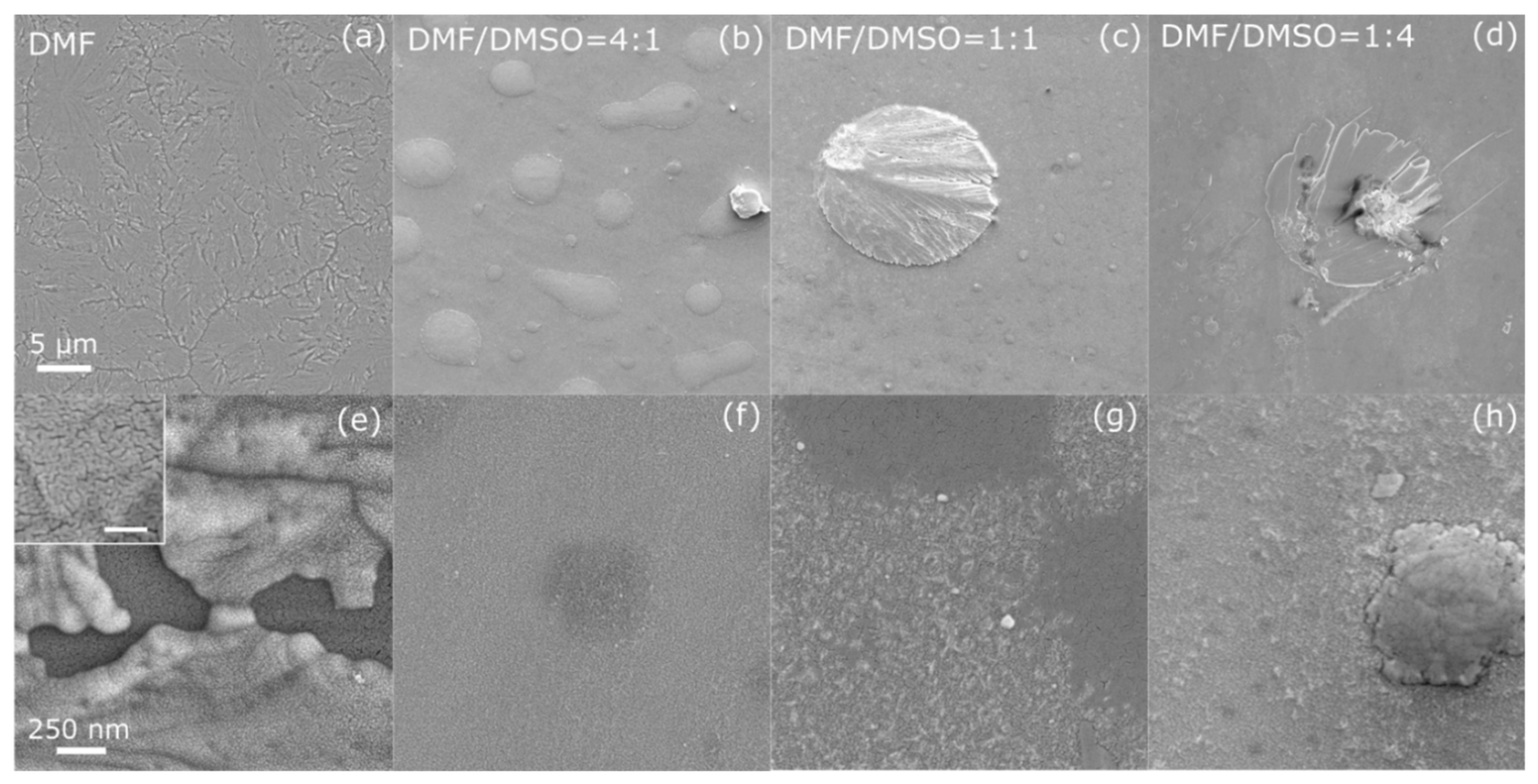
Abstract
:1. Introduction
2. Materials and Methods
2.1. Film Preparation
2.2. Annealing, Aging and Exposition to Controlled Humidity Environment
2.3. Photodegradation Experiments
2.4. Scanning Electron Microscopy
2.5. Grazing Incidence X–ray Diffraction (GIXD) and Specular XRD
2.6. Optical Measurements
3. Results and Discussion
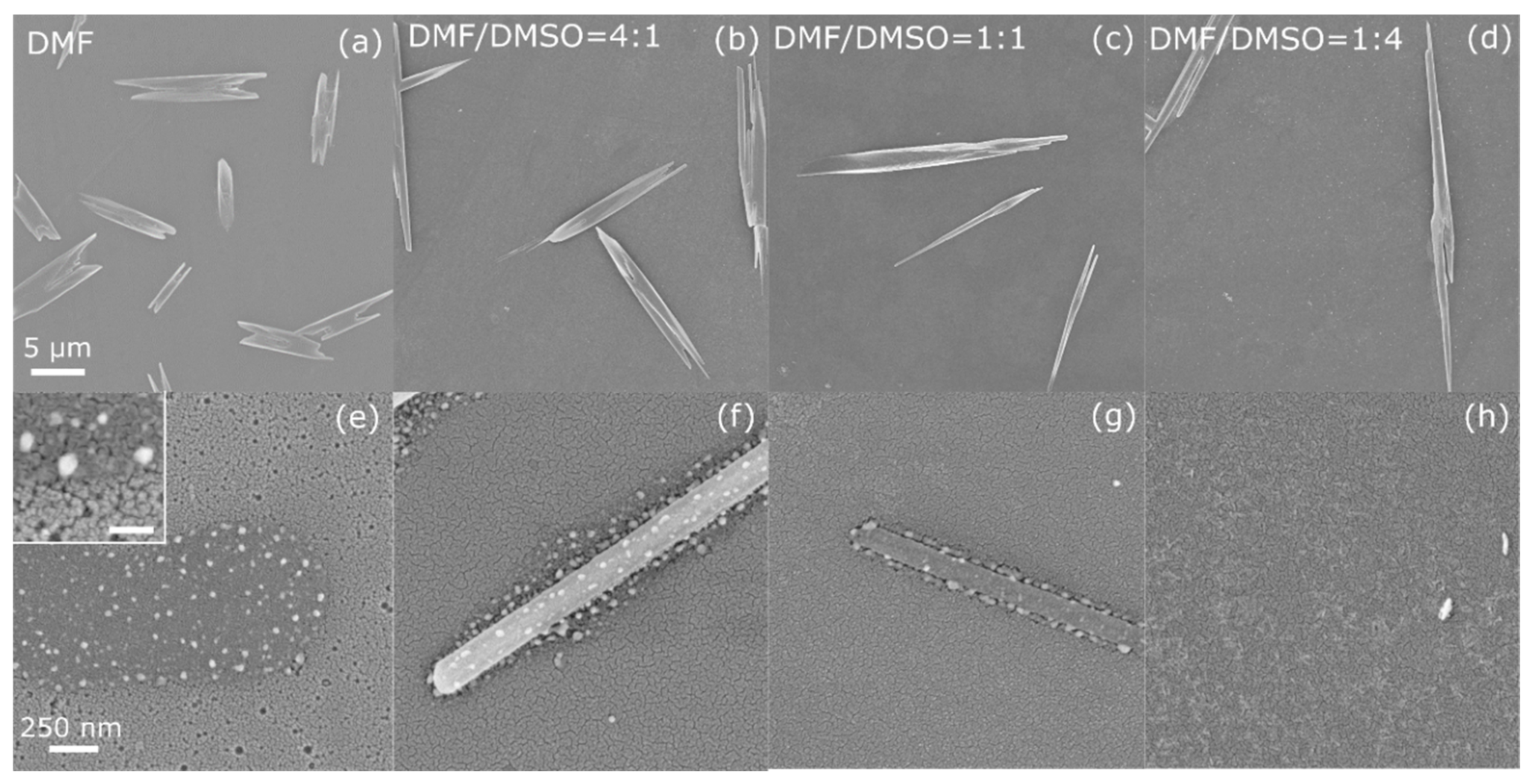
3.1. Morphology of the As-Deposited (PRSH)PbX3 Thin Films
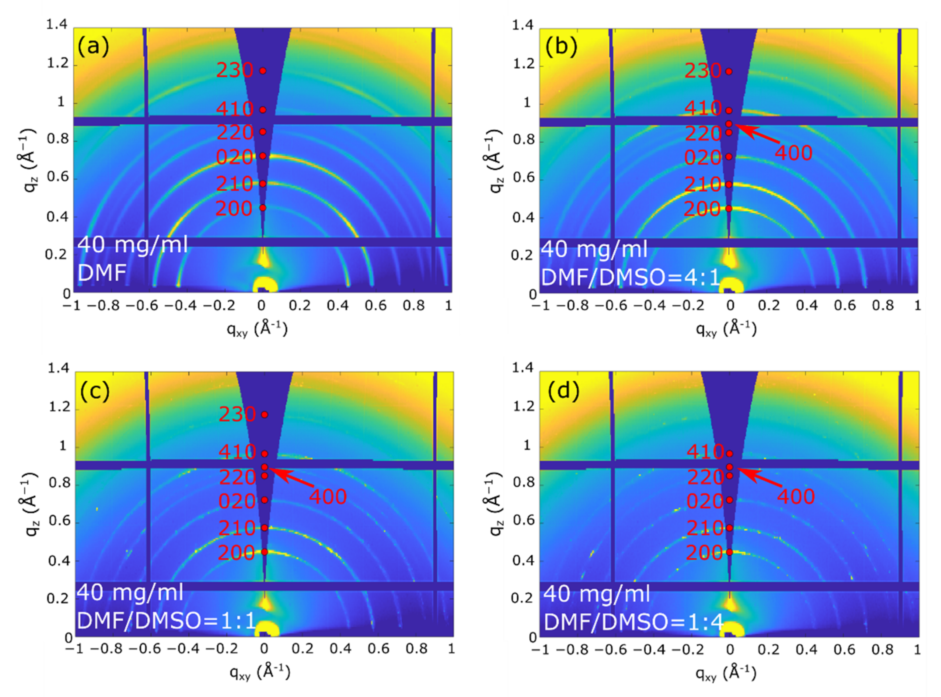
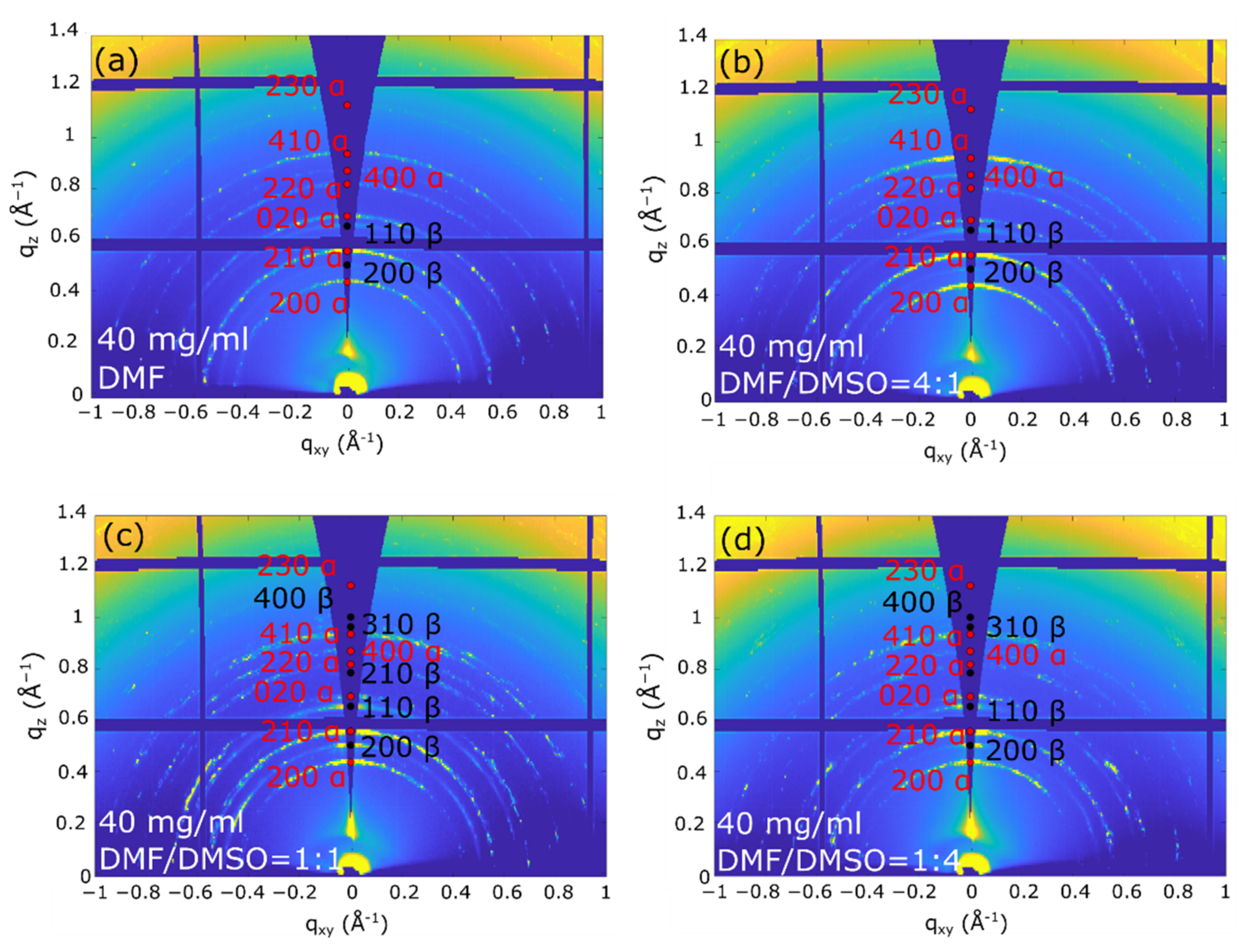
3.2. Structure and Texture of (PRSH)PbX3 Thin Films
3.2.1. Crystal Phase and Compositional Analysis
3.2.2. Texturing
3.3. Effects of Thermal Annealing
3.3.1. Ex-Situ Annealing
3.3.2. In-Situ Annealing
3.4. Effect of Film Aging
3.5. Effect of UV Light Exposure
3.6. Stability of Thin Films in a Controlled Humidity Environment
4. Conclusions
Supplementary Materials
Author Contributions
Funding
Institutional Review Board Statement
Informed Consent Statement
Data Availability Statement
Acknowledgments
Conflicts of Interest
References
- Jeong, J.; Kim, M.; Seo, J.; Lu, H.; Ahlawat, P.; Mishra, A.; Yang, Y.; Hope, M.A.; Eickemeyer, F.T.; Kim, M.; et al. Pseudo-Halide Anion Engineering for α-FAPbI 3 Perovskite Solar Cells. Nature 2021, 592, 381–385. [Google Scholar] [CrossRef] [PubMed]
- Stranks, S.D.; Eperon, G.E.; Grancini, G.; Menelaou, C.; Alcocer, M.J.P.; Leijtens, T.; Herz, L.M.; Petrozza, A.; Snaith, H.J. Electron-Hole Diffusion Lengths Exceeding 1 Micrometer in an Organometal Trihalide Perovskite Absorber. Science 2013, 342, 341–344. [Google Scholar] [CrossRef] [Green Version]
- Oga, H.; Saeki, A.; Ogomi, Y.; Hayase, S.; Seki, S. Improved Understanding of the Electronic and Energetic Landscapes of Perovskite Solar Cells: High Local Charge Carrier Mobility, Reduced Recombination, and Extremely Shallow Traps. J. Am. Chem. Soc. 2014, 136, 13818–13825. [Google Scholar] [CrossRef] [PubMed]
- Wang, Y.; Zhang, Y.; Zhang, P.; Zhang, W. High Intrinsic Carrier Mobility and Photon Absorption in the Perovskite CH3NH3PbI. Phys. Chem. Chem. Phys. 2015, 17, 11516–11520. [Google Scholar] [CrossRef] [PubMed]
- Ghasdi, M.; Alamdari, H. CO Sensitive Nanocrystalline LaCoO3 Perovskite Sensor Prepared by High Energy Ball Milling. Sens. Actuators B Chem. 2010, 148, 478–485. [Google Scholar] [CrossRef]
- Yu, W.; Li, F.; Yu, L.; Niazi, M.R.; Zou, Y.; Corzo, D.; Basu, A.; Ma, C.; Dey, S.; Tietze, M.L.; et al. Single Crystal Hybrid Perovskite Field-Effect Transistors. Nat. Commun. 2018, 9, 5354. [Google Scholar] [CrossRef] [PubMed] [Green Version]
- Mettan, X.; Pisoni, R.; Matus, P.; Pisoni, A.; Jaćimović, J.; Náfrádi, B.; Spina, M.; Pavuna, D.; Forró, L.; Horváth, E. Tuning of the Thermoelectric Figure of Merit of CH3NH3MI3 (M = Pb,Sn) Photovoltaic Perovskites. J. Phys. Chem. C 2015, 119, 11506–11510. [Google Scholar] [CrossRef] [Green Version]
- Jella, V.; Ippili, S.; Eom, J.-H.; Pammi, S.V.N.; Jung, J.-S.; Tran, V.-D.; Nguyen, V.H.; Kirakosyan, A.; Yun, S.; Kim, D.; et al. A Comprehensive Review of Flexible Piezoelectric Generators Based on Organic-Inorganic Metal Halide Perovskites. Nano Energy 2019, 57, 74–93. [Google Scholar] [CrossRef]
- Veldhuis, S.A.; Boix, P.P.; Yantara, N.; Li, M.; Sum, T.C.; Mathews, N.; Mhaisalkar, S.G. Perovskite Materials for Light-Emitting Diodes and Lasers. Adv. Mater. 2016, 28, 6804–6834. [Google Scholar] [CrossRef]
- Zhu, H.; Fu, Y.; Meng, F.; Wu, X.; Gong, Z.; Ding, Q.; Gustafsson, M.V.; Trinh, M.T.; Jin, S.; Zhu, X.-Y. Lead Halide Perovskite Nanowire Lasers with Low Lasing Thresholds and High Quality Factors. Nat. Mater 2015, 14, 636–642. [Google Scholar] [CrossRef]
- Dou, L.; Yang, Y.; You, J.; Hong, Z.; Chang, W.-H.; Li, G.; Yang, Y. Solution-Processed Hybrid Perovskite Photodetectors with High Detectivity. Nat. Commun. 2014, 5, 5404. [Google Scholar] [CrossRef]
- Boyd, C.C.; Cheacharoen, R.; Leijtens, T.; McGehee, M.D. Understanding Degradation Mechanisms and Improving Stability of Perovskite Photovoltaics. Chem. Rev. 2019, 119, 3418–3451. [Google Scholar] [CrossRef]
- Christians, J.A.; Habisreutinger, S.N.; Berry, J.J.; Luther, J.M. Stability in Perovskite Photovoltaics: A Paradigm for Newfangled Technologies. ACS Energy Lett. 2018, 3, 2136–2143. [Google Scholar] [CrossRef] [Green Version]
- Conings, B.; Drijkoningen, J.; Gauquelin, N.; Babayigit, A.; D’Haen, J.; D’Olieslaeger, L.; Ethirajan, A.; Verbeeck, J.; Manca, J.; Mosconi, E.; et al. Intrinsic Thermal Instability of Methylammonium Lead Trihalide Perovskite. Adv. Energy Mater. 2015, 5, 1500477. [Google Scholar] [CrossRef]
- Soe, C.M.M.; Nie, W.; Stoumpos, C.C.; Tsai, H.; Blancon, J.-C.; Liu, F.; Even, J.; Marks, T.J.; Mohite, A.D.; Kanatzidis, M.G. Understanding Film Formation Morphology and Orientation in High Member 2D Ruddlesden–Popper Perovskites for High-Efficiency Solar Cells. Adv. Energy Mater. 2018, 8, 1700979. [Google Scholar] [CrossRef]
- Lai, H.; Kan, B.; Liu, T.; Zheng, N.; Xie, Z.; Zhou, T.; Wan, X.; Zhang, X.; Liu, Y.; Chen, Y. Two-Dimensional Ruddlesden–Popper Perovskite with Nanorod-like Morphology for Solar Cells with Efficiency Exceeding 15%. J. Am. Chem. Soc. 2018, 140, 11639–11646. [Google Scholar] [CrossRef]
- Quan, L.N.; Yuan, M.; Comin, R.; Voznyy, O.; Beauregard, E.M.; Hoogland, S.; Buin, A.; Kirmani, A.R.; Zhao, K.; Amassian, A.; et al. Ligand-Stabilized Reduced-Dimensionality Perovskites. J. Am. Chem. Soc. 2016, 138, 2649–2655. [Google Scholar] [CrossRef] [Green Version]
- Grancini, G.; Roldán-Carmona, C.; Zimmermann, I.; Mosconi, E.; Lee, X.; Martineau, D.; Narbey, S.; Oswald, F.; De Angelis, F.; Graetzel, M.; et al. One-Year Stable Perovskite Solar Cells by 2D/3D Interface Engineering. Nat. Commun. 2017, 8, 15684. [Google Scholar] [CrossRef]
- Chen, P.; Bai, Y.; Wang, S.; Lyu, M.; Yun, J.-H.; Wang, L. In Situ Growth of 2D Perovskite Capping Layer for Stable and Efficient Perovskite Solar Cells. Adv. Funct. Mater. 2018, 28, 1706923. [Google Scholar] [CrossRef]
- Lin, H.; Zhou, C.; Tian, Y.; Siegrist, T.; Ma, B. Low-Dimensional Organometal Halide Perovskites. ACS Energy Lett. 2018, 3, 54–62. [Google Scholar] [CrossRef] [Green Version]
- Gao, L.; Spanopoulos, I.; Ke, W.; Huang, S.; Hadar, I.; Chen, L.; Li, X.; Yang, G.; Kanatzidis, M.G. Improved Environmental Stability and Solar Cell Efficiency of (MA,FA)PbI3 Perovskite Using a Wide-Band-Gap 1D Thiazolium Lead Iodide Capping Layer Strategy. ACS Energy Lett. 2019, 4, 1763–1769. [Google Scholar] [CrossRef]
- Liu, P.; Xian, Y.; Yuan, W.; Long, Y.; Liu, K.; Rahman, N.U.; Li, W.; Fan, J. Lattice-Matching Structurally-Stable 1D@3D Perovskites toward Highly Efficient and Stable Solar Cells. Adv. Energy Mater. 2020, 10, 1903654. [Google Scholar] [CrossRef]
- Yang, X.; Ma, L.-F.; Yan, D. Facile Synthesis of 1D Organic–Inorganic Perovskite Micro-Belts with High Water Stability for Sensing and Photonic Applications. Chem. Sci. 2019, 10, 4567–4572. [Google Scholar] [CrossRef] [Green Version]
- Zheng, X.; Zhao, W.; Wang, P.; Tan, H.; Saidaminov, M.I.; Tie, S.; Chen, L.; Peng, Y.; Long, J.; Zhang, W.-H. Ultrasensitive and Stable X-Ray Detection Using Zero-Dimensional Lead-Free Perovskites. J. Energy Chem. 2020, 49, 299–306. [Google Scholar] [CrossRef]
- Ma, C.; Shen, D.; Huang, B.; Li, X.; Chen, W.-C.; Lo, M.-F.; Wang, P.; Lam, M.H.-W.; Lu, Y.; Ma, B.; et al. High Performance Low-Dimensional Perovskite Solar Cells Based on a One Dimensional Lead Iodide Perovskite. J. Mater. Chem. A 2019, 7, 8811–8817. [Google Scholar] [CrossRef]
- Pipitone, C.; Giannici, F.; Martorana, A.; Bertolotti, F.; Calabrese, G.; Milita, S.; Guagliardi, A.; Masciocchi, N. Proton Sponge Lead Halides Containing 1D Polyoctahedral Chains. CrystEngComm 2021, 23, 1126–1139. [Google Scholar] [CrossRef]
- Ava, T.T.; Al Mamun, A.; Marsillac, S.; Namkoong, G. A Review: Thermal Stability of Methylammonium Lead Halide Based Perovskite Solar Cells. Appl. Sci. 2019, 9, 188. [Google Scholar] [CrossRef] [Green Version]
- Fan, Y.; Meng, H.; Wang, L.; Pang, S. Review of Stability Enhancement for Formamidinium-Based Perovskites. Sol. RRL 2019, 3, 1900215. [Google Scholar] [CrossRef]
- Pool, V.L.; Dou, B.; Van Campen, D.G.; Klein-Stockert, T.R.; Barnes, F.S.; Shaheen, S.E.; Ahmad, M.I.; van Hest, M.F.A.M.; Toney, M.F. Thermal Engineering of FAPbI3 Perovskite Material via Radiative Thermal Annealing and in Situ XRD. Nat. Commun. 2017, 8, 14075. [Google Scholar] [CrossRef] [PubMed] [Green Version]
- Pozharskii, A.F. Naphthalene’proton sponges. Russ. Chem. Rev. 1998, 67, 1–24. [Google Scholar] [CrossRef]
- Kahoul, A.; Hammouche, A.; Naamoune, F.; Chartier, P.; Poillerat, G.; Koenig, J.F. Solvent Effect on Synthesis of Perovskite-Type La1ϪxCaxCoO3 and Their Electrochemical Properties for Oxygen Reactions. Mater. Res. Bull. 2000, 35, 12. [Google Scholar]
- Chen, H.; Wei, Z.; He, H.; Zheng, X.; Wong, K.S.; Yang, S. Solvent Engineering Boosts the Efficiency of Paintable Carbon-Based Perovskite Solar Cells to Beyond 14%. Adv. Energy Mater. 2016, 6, 1502087. [Google Scholar] [CrossRef]
- Ren, Y.-K.; Liu, S.-D.; Duan, B.; Xu, Y.-F.; Li, Z.-Q.; Huang, Y.; Hu, L.-H.; Zhu, J.; Dai, S.-Y. Controllable Intermediates by Molecular Self-Assembly for Optimizing the Fabrication of Large-Grain Perovskite Films via One-Step Spin-Coating. J. Alloy. Compd. 2017, 705, 205–210. [Google Scholar] [CrossRef]
- Lim, G.; Parrish, W.; Ortiz, C.; Bellotto, M.; Hart, M. Grazing Incidence Synchrotron X-Ray Diffraction Method for Analyzing Thin Films. J. Mater. Res. 1987, 2, 471–477. [Google Scholar] [CrossRef]
- Fewster, P.F. X-Ray Analysis of Thin Films and Multilayers. Rep. Prog. Phys. 1996, 59, 1339–1407. [Google Scholar] [CrossRef]
- Schneider, C.A.; Rasband, W.S.; Eliceiri, K.W. NIH Image to ImageJ: 25 Years of Image Analysis. Nat. Methods 2012, 9, 671–675. [Google Scholar] [CrossRef]
- Schrode, B.; Pachmajer, S.; Dohr, M.; Röthel, C.; Domke, J.; Fritz, T.; Resel, R.; Werzer, O. GIDVis: A Comprehensive Software Tool for Geometry-Independent Grazing-Incidence X-Ray Diffraction Data Analysis and Pole-Figure Calculations. J Appl Cryst. 2019, 52, 683–689. [Google Scholar] [CrossRef] [Green Version]
- Hao, F.; Stoumpos, C.C.; Guo, P.; Zhou, N.; Marks, T.J.; Chang, R.P.H.; Kanatzidis, M.G. Solvent-Mediated Crystallization of CH3NH3SnI3 Films for Heterojunction Depleted Perovskite Solar Cells. J. Am. Chem. Soc. 2015, 137, 11445–11452. [Google Scholar] [CrossRef]
- Wu, C.; Wang, K.; Li, J.; Liang, Z.; Li, J.; Li, W.; Zhao, L.; Chi, B.; Wang, S. Volatile Solution: The Way toward Scalable Fabrication of Perovskite Solar Cells? Matter 2021, 4, 775–793. [Google Scholar] [CrossRef]
- Pascoe, A.R.; Gu, Q.; Rothmann, M.U.; Li, W.; Zhang, Y.; Scully, A.D.; Lin, X.; Spiccia, L.; Bach, U.; Cheng, Y.B. Directing Nucleation and Growth Kinetics in Solution-Processed Hybrid Perovskite Thin-Films. Sci. China Mater. 2017, 60, 617–628. [Google Scholar] [CrossRef] [Green Version]
- Wu, Y.; Islam, A.; Yang, X.; Qin, C.; Liu, J.; Zhang, K.; Peng, W.; Han, L. Retarding the Crystallization of PbI2 for Highly Reproducible Planar-Structured Perovskite Solar Cells via Sequential Deposition. Energy Environ. Sci. 2014, 7, 2934–2938. [Google Scholar] [CrossRef]
- Ahn, N.; Son, D.-Y.; Jang, I.-H.; Kang, S.M.; Choi, M.; Park, N.-G. Highly Reproducible Perovskite Solar Cells with Average Efficiency of 18.3% and Best Efficiency of 19.7% Fabricated via Lewis Base Adduct of Lead(II) Iodide. J. Am. Chem. Soc. 2015, 137, 8696–8699. [Google Scholar] [CrossRef]
- Zhao, H.; Liu, X.; Xu, J.; Li, Z.; Fu, Y.; Zhu, H.; Yan, L.; Liu, Z.; Liu, S.F.; Yao, J. Improvement of Colloidal Characteristics in a Precursor Solution by a PbI2-(DMSO)2 Complex for Efficient Nonstoichiometrically Prepared CsPbI2.8Br0.2 Perovskite Solar Cells. ACS Appl. Mater. Interfaces 2020, 12, 48756–48764. [Google Scholar] [CrossRef]
- Kim, H.-B.; Choi, H.; Jeong, J.; Kim, S.; Walker, B.; Song, S.; Kim, J.Y. Mixed Solvents for the Optimization of Morphology in Solution-Processed, Inverted-Type Perovskite/Fullerene Hybrid Solar Cells. Nanoscale 2014, 6, 6679–6683. [Google Scholar] [CrossRef]
- Yu, J.C.; Kim, D.B.; Jung, E.D.; Lee, B.R.; Song, M.H. High-Performance Perovskite Light-Emitting Diodes via Morphological Control of Perovskite Films. Nanoscale 2016, 8, 7036–7042. [Google Scholar] [CrossRef] [Green Version]
- Pfattner, R.; Mas-Torrent, M.; Bilotti, I.; Brillante, A.; Milita, S.; Liscio, F.; Biscarini, F.; Marszalek, T.; Ulanski, J.; Nosal, A.; et al. High-Performance Single Crystal Organic Field-Effect Transistors Based on Two Dithiophene-Tetrathiafulvalene (DT-TTF) Polymorphs. Adv. Mater. 2010, 22, 4198–4203. [Google Scholar] [CrossRef]
- Milita, S.; Liscio, F.; Cowen, L.; Cavallini, M.; Drain, B.A.; Degousée, T.; Luong, S.; Fenwick, O.; Guagliardi, A.; Schroeder, B.C.; et al. Polymorphism in N,N′-Dialkyl-Naphthalene Diimides. J. Mater. Chem. C 2020, 8, 3097–3112. [Google Scholar] [CrossRef]
- Yuan, Z.; Zhou, C.; Tian, Y.; Shu, Y.; Messier, J.; Wang, J.C.; van de Burgt, L.J.; Kountouriotis, K.; Xin, Y.; Holt, E.; et al. One-Dimensional Organic Lead Halide Perovskites with Efficient Bluish White-Light Emission. Nat. Commun. 2017, 8, 14051. [Google Scholar] [CrossRef]
- Hangoma, P.M.; Shin, I.; Yang, H.-S.; Kim, D.; Jung, Y.K.; Lee, B.R.; Kim, J.H.; Kim, K.H.; Park, S.H. 2D Perovskite Seeding Layer for Efficient Air-Processable and Stable Planar Perovskite Solar Cells. Adv. Funct. Mater. 2020, 30, 2003081. [Google Scholar] [CrossRef]
- Wang, J.; Fang, C.; Ma, J.; Wang, S.; Jin, L.; Li, W.; Li, D. Aqueous Synthesis of Low-Dimensional Lead Halide Perovskites for Room-Temperature Circularly Polarized Light Emission and Detection. ACS Nano 2019, 13, 9473–9481. [Google Scholar] [CrossRef]
- Macrae, C.F.; Sovago, I.; Cottrell, S.J.; Galek, P.T.A.; McCabe, P.; Pidcock, E.; Platings, M.; Shields, G.P.; Stevens, J.S.; Towler, M.; et al. Mercury 4.0: From Visualization to Analysis, Design and Prediction. J. Appl. Cryst. 2020, 53, 226–235. [Google Scholar] [CrossRef] [PubMed] [Green Version]
- Abbinante, V.M.; García-Espejo, G.; Calabrese, G.; Milita, S.; Barba, L.; Marini, D.; Pipitone, C.; Giannici, F.; Guagliardi, A.; Masciocchi, N. Conformationally Rigid Molecular and Polymeric Naphthalene-Diimides Containing C6H6N2 Constitutional Isomers. J. Mater. Chem. C 2021, 9, 10875–10888. [Google Scholar] [CrossRef]
- Niu, T.; Xue, Q.; Yip, H.-L. Advances in Dion-Jacobson Phase Two-Dimensional Metal Halide Perovskite Solar Cells. Nanophotonics 2020, 10, 2069–2102. [Google Scholar] [CrossRef]
- Zheng, G.; Zhu, C.; Ma, J.; Zhang, X.; Tang, G.; Li, R.; Chen, Y.; Li, L.; Hu, J.; Hong, J.; et al. Manipulation of Facet Orientation in Hybrid Perovskite Polycrystalline Films by Cation Cascade. Nat. Commun. 2018, 9, 2793. [Google Scholar] [CrossRef] [Green Version]
- Brunova, A.; Vegso, K.; Nadazdy, V.; Nadazdy, P.; Subair, R.; Jergel, M.; Majkova, E.; Pandit, P.; Roth, S.V.; Krasnansky, A.; et al. Structural and Trap-State Density Enhancement in Flash Infrared Annealed Perovskite Layers. Adv. Mater. Interfaces 2021, 8, 2100355. [Google Scholar] [CrossRef]
- Misra, R.K.; Ciammaruchi, L.; Aharon, S.; Mogilyansky, D.; Etgar, L.; Visoly-Fisher, I.; Katz, E.A. Effect of Halide Composition on the Photochemical Stability of Perovskite Photovoltaic Materials. ChemSusChem 2016, 9, 2572. [Google Scholar] [CrossRef] [Green Version]
- Krishnan, U.; Kaur, M.; Kumar, M.; Kumar, A. Factors Affecting the Stability of Perovskite Solar Cells: A Comprehensive Review. JPE 2019, 9, 021001. [Google Scholar]
- Wasserman, H.J.; Vermaak, J.S. On the Determination of the Surface Stress of Copper and Platinum. Surf. Sci. 1972, 32, 168–174. [Google Scholar] [CrossRef]
- Diehm, P.M.; Ágoston, P.; Albe, K. Size-Dependent Lattice Expansion in Nanoparticles: Reality or Anomaly? Chemphyschem 2012, 13, 2443–2454. [Google Scholar] [CrossRef]
- Calabrese, G.; van Treeck, D.; Kaganer, V.M.; Konovalov, O.; Corfdir, P.; Sinito, C.; Geelhaar, L.; Brandt, O.; Fernández-Garrido, S. Radius-Dependent Homogeneous Strain in Uncoalesced GaN Nanowires. Acta Mater. 2020, 195, 87–97. [Google Scholar] [CrossRef]
- Zhou, N.; Huang, B.; Sun, M.; Zhang, Y.; Li, L.; Lun, Y.; Wang, X.; Hong, J.; Chen, Q.; Zhou, H. The Spacer Cations Interplay for Efficient and Stable Layered 2D Perovskite Solar Cells. Adv. Energy Mater. 2020, 10, 1901566. [Google Scholar] [CrossRef]
- Wang, X.; Rakstys, K.; Jack, K.; Jin, H.; Lai, J.; Li, H.; Ranasinghe, C.S.K.; Saghaei, J.; Zhang, G.; Burn, P.L.; et al. Engineering Fluorinated-Cation Containing Inverted Perovskite Solar Cells with an Efficiency of >21% and Improved Stability towards Humidity. Nat. Commun. 2021, 12, 52. [Google Scholar] [CrossRef]
- Misra, R.K.; Aharon, S.; Li, B.; Mogilyansky, D.; Visoly-Fisher, I.; Etgar, L.; Katz, E.A. Temperature-and component-dependent degradation of perovskite photovoltaic materials under concentrated sunlight. J. Phys. Chem. Lett. 2015, 6, 326–330. [Google Scholar] [CrossRef]
- Zhang, Y.; Li, S.; Li, Z.; Liu, H.; Liu, X.; Chen, J.; Fang, X. High-Performance Two-Dimensional Perovskite Ca2Nb3O10 UV Photodetectors. Nano Lett. 2020, 21, 382–388. [Google Scholar] [CrossRef]
- Yang, J.; Kang, W.; Liu, Z.; Pi, M.; Luo, L.B.; Li, C.; Lin, H.; Luo, Z.; Du, J.; Zhou, M.; et al. High-performance deep ultraviolet photodetector based on a one-dimensional lead-free halide perovskite CsCu2I3 film with high stability. J. Phys. Chem. Lett. 2020, 11, 6880–6886. [Google Scholar] [CrossRef]
- Wang, S.; Chen, Y.; Yao, J.; Zhao, G.; Li, L.; Zou, G. Wafer-sized 2D perovskite single crystal thin films for UV photodetectors. J. Mat. Chem. C 2021, 9, 6498–6506. [Google Scholar] [CrossRef]
- Sharma, S.K.; Phadnis, C.; Das, T.K.; Kumar, A.; Kavaipatti, B.; Chowdhury, A.; Yella, A. Reversible Dimensionality Tuning of Hybrid Perovskites with Humidity: Visualization and Application to Stable Solar Cells. Chem. Mater. 2019, 31, 3111–3117. [Google Scholar] [CrossRef]
- McGovern, L.; Futscher, M.H.; Muscarella, L.A.; Ehrler, B. Understanding the Stability of MAPbBr3 versus MAPbI3: Suppression of Methylammonium Migration and Reduction of Halide Migration. J. Phys. Chem. Lett. 2020, 11, 7127–7132. [Google Scholar] [CrossRef]


Publisher’s Note: MDPI stays neutral with regard to jurisdictional claims in published maps and institutional affiliations. |
© 2021 by the authors. Licensee MDPI, Basel, Switzerland. This article is an open access article distributed under the terms and conditions of the Creative Commons Attribution (CC BY) license (https://creativecommons.org/licenses/by/4.0/).
Share and Cite
Calabrese, G.; Pipitone, C.; Marini, D.; Giannici, F.; Martorana, A.; Barba, L.; Summonte, C.; Masciocchi, N.; Milita, S. Highly Stable Thin Films Based on Novel Hybrid 1D (PRSH)PbX3 Pseudo-Perovskites. Nanomaterials 2021, 11, 2765. https://doi.org/10.3390/nano11102765
Calabrese G, Pipitone C, Marini D, Giannici F, Martorana A, Barba L, Summonte C, Masciocchi N, Milita S. Highly Stable Thin Films Based on Novel Hybrid 1D (PRSH)PbX3 Pseudo-Perovskites. Nanomaterials. 2021; 11(10):2765. https://doi.org/10.3390/nano11102765
Chicago/Turabian StyleCalabrese, Gabriele, Candida Pipitone, Diego Marini, Francesco Giannici, Antonino Martorana, Luisa Barba, Caterina Summonte, Norberto Masciocchi, and Silvia Milita. 2021. "Highly Stable Thin Films Based on Novel Hybrid 1D (PRSH)PbX3 Pseudo-Perovskites" Nanomaterials 11, no. 10: 2765. https://doi.org/10.3390/nano11102765