Article

Multi-Level Analog Resistive Switching Characteristics in Tri-Layer HfO2/Al2O3/HfO2 Based Memristor on ITO Electrode

1
School of Electronics Engineering, Chungbuk National University, Cheongju 28644, Korea
2
Department of Electronics Engineering, Korea National University of Transportation, Chungju-si 27469, Korea
3
Division of Electronics and Electrical Engineering, Dongguk University, Seoul 04620, Korea
*
Authors to whom correspondence should be addressed.
Nanomaterials 2020, 10(10), 2069; https://doi.org/10.3390/nano10102069
Submission received: 6 September 2020 / Revised: 25 September 2020 / Accepted: 16 October 2020 / Published: 20 October 2020

Abstract

:
Atomic layer deposited (ALD) HfO2/Al2O3/HfO2 tri-layer resistive random access memory (RRAM) structure has been studied with a transparent indium tin oxide (ITO) transparent electrode. Highly stable and reliable multilevel conductance can be controlled by the set current compliance and reset stop voltage in bipolar resistive switching. Improved gradual resistive switching was achieved because of the interdiffusion in the HfO2/Al2O3 interface where tri-valent Al incorporates with HfO2 and produces HfAlO. The uniformity in bipolar resistive switching with Ion/Ioff ratio (>10) and excellent endurance up to >103 cycles was achieved. Multilevel conductance levels in potentiation/depression were realized with constant amplitude pulse train and increasing pulse amplitude. Thus, tri-layer structure-based RRAM can be a potential candidate for the synaptic device in neuromorphic computing.

1. Introduction

The physical limitation of the conventional flash memory gives rise to the development of resistive random access memory (RRAM) due to its low power consumption, higher density, and simple structure, which consist of mainly transition metal oxides sandwiched between the top and bottom electrodes [1,2,3,4,5,6]. Although, single layer RRAM devices have been found to have uncontrolled filament formation and high switching voltage [7,8,9]. Therefore, research has been focused on gaining low-power RRAM devices for symmetric SET/RESET behavior, gradual conductance change, and high synaptic density. Transition metal oxide, mainly based on Al2O3, HfO2, TaOx, ZrO2, TiO2, and their bilayer and tri-layer structure, was shown to be advantageous for industry-friendly electrical devices and improved multilevel resistive switching properties and its application towards synapses for neuromorphic computing [10,11,12,13,14,15,16].
Bilayer RRAM structures already have shown both abrupt and gradual change in conductance under bipolar resistive switching, which has been proposed effective for neuromorphic computing with tunable potentiation and depression. Among different bilayer structures, recently Al2O3/Ta2O5, HfOx/HfO2, HfO2/TiOx, TaOx/Al2O3, Al2O3/TiO2 have been proposed to modulate the RRAM conductance gradually during resistive switching [5,13,17,18,19]. In bilayer structures mostly, oxygen vacancies were found to be located at the bilayer interface, thus the push and pull of oxygen vacancies from the interface mainly controls the resistance of the device during switching. Additionally, in other devices, modulation of the conductance can be controlled by the motion of oxygen vacancies between oxygen-deficient and oxygen-rich layers, which further limits the device’s operation current and controls low power consumption in RRAM. On the other hand, related to the multi-layer resistive switching, Wang et al., described the tri-layer RRAM structure of Al2O3/HfO2/Al2O3 with abrupt resistive switching performance [20]. In this work, it is considered that the concentration of oxygen vacancy is higher in HfO2 compared to Al2O3 and interfacial diffusion took place between two dielectrics. Therefore, the interfacial layer helps to exchange oxygen vacancies (VO), which finally improves resistive switching. A similar phenomenon has been indicated by Lui et al., where multilevel conductance was modulated by VReset-stop in Al2O3/HfO2/Al2O3 RRAM structure [21]. In the case of unipolar resistive switching, an important finding was explained by Maestro-Izquierdo et al., where 3D simulation suggests that during the RESET process, temperature distributions are different in multilayer structures [22]. Abrupt switching took place due to conductive filament (CF) narrowing in the HfO2 middle layer due to lower thermal conductivity of HfO2 (1.0 W m−1 K−1) compared to Al2O3 (2.86 W m−1 K−1) [23]. Furthermore, the tri-layer formed by inserting an oxygen-deficient ZrO2‒x layer between two ZrO2 dielectric layers was found to have transitioned from interfacial to filamentary switching characteristics under different SET compliance currents [24]. However, it has previously been reported that the VO from CF has low mobility in the AlOx layer compared to HfO2 during the reset operation [25]. As compared to other different tri-layer RRAM structures mentioned above, for tri-layer RRAM structure in this study, the Al2O3 layer is placed between two higher Vo contents in HfO2 layers for better movement of the Vo during SET and RESET operations. In addition, the virtual electrode formed during the electroforming process within Vo rich HfO2 layers at both ends can help the CF regrowth during SET operation at lower electric field [26].
For the next generation of electronic devices, transparent electronics are recently emerging [27,28,29]. The development of transparent electronics including touch panel, display, energy storage, photodetector, and solar cells have attracted great interest. RRAM on transparent electrodes such as indium tin oxide (ITO), with gradual multilevel resistive switching for logic and memory devices, has gained increasing attention as a reliable synaptic device. Hence, it is highly expected that future RRAM embedded with transparent electrode (ITO) will become a paradigm for future see-through memory devices.
In this work, the proposed atomic layer deposited (ALD) HfO2/Al2O3/HfO2 tri-layer RRAM structure with a transparent ITO electrode has been studied in detail, which is believed to be more suitable for multilevel resistive switching. In addition, considering HfO2 has larger oxygen vacancies compared to Al2O3, this structure has been designed to have two interlayers formed between the top and bottom HfO2 layers with a middle Al2O3 layer. Excellent multi-resistance states were achieved for tri-layer RRAM to emulate neuromorphic properties. For application in synaptic devices, multilevel conductance was achieved by applying both DC and pulse voltages.

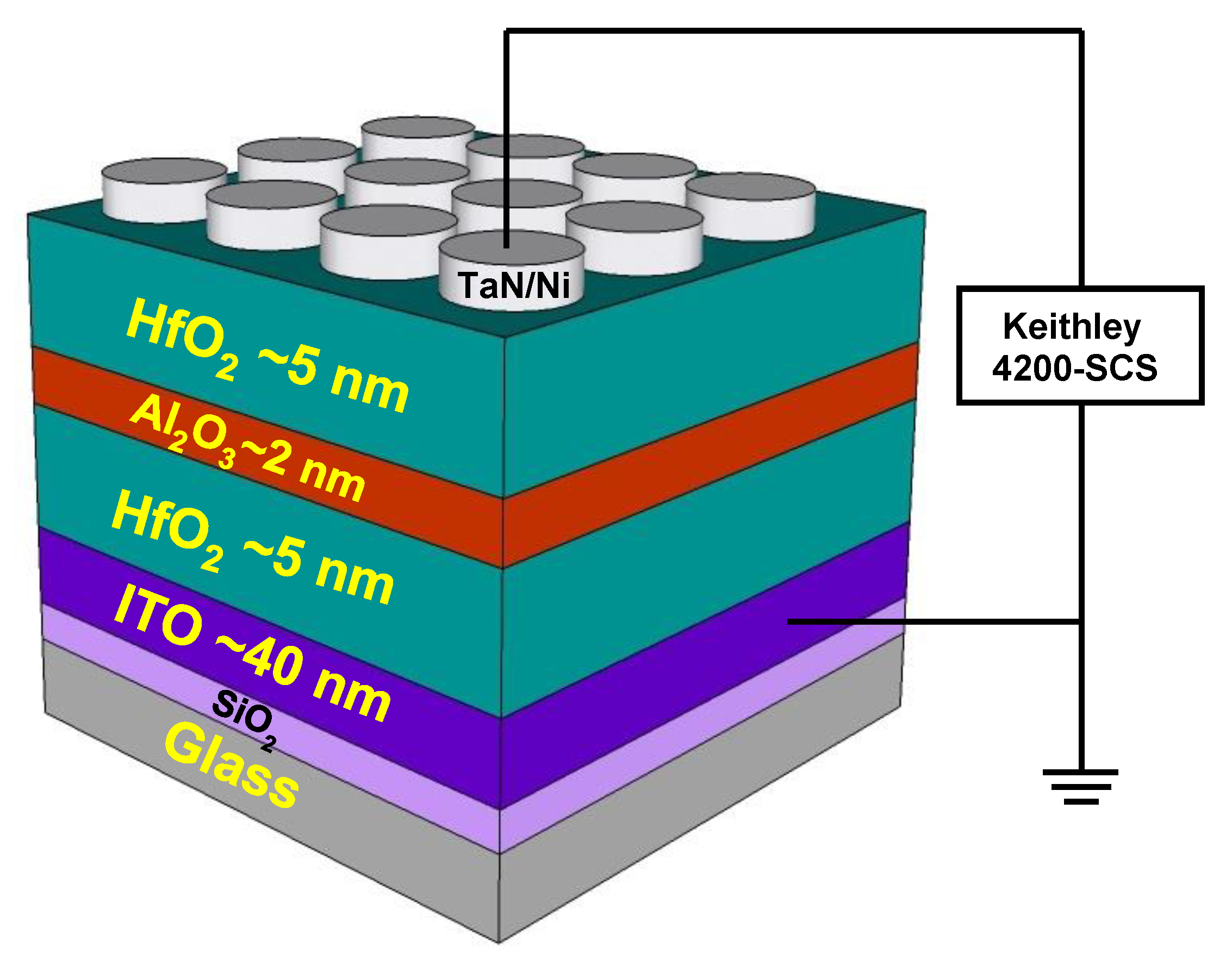
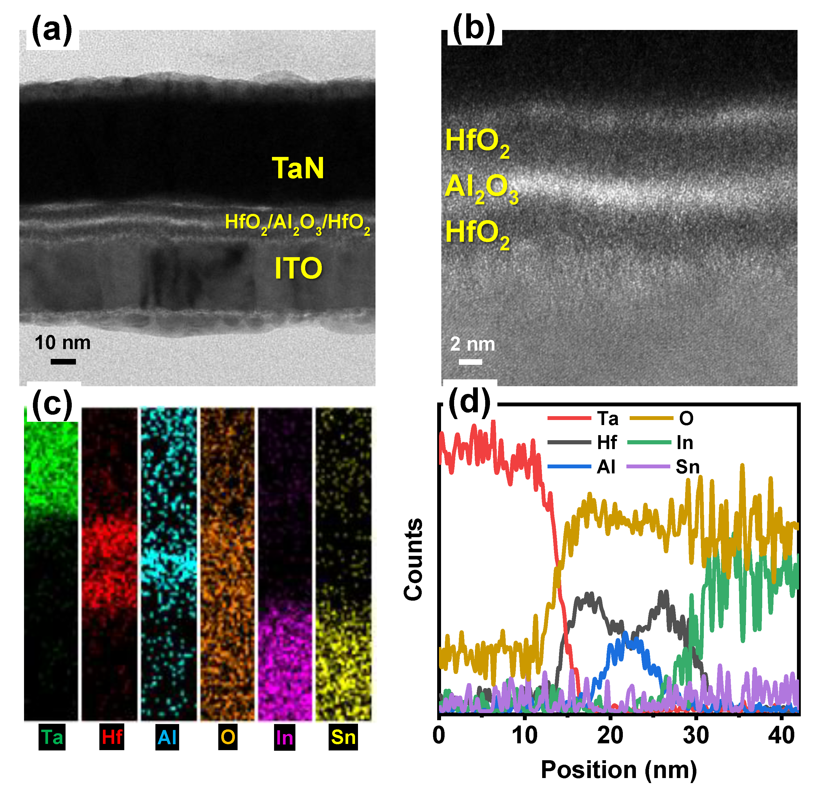
2. Materials and Methods

Initially, the bottom electrode was taken as commercially available ~40-nm-thick ITO (sheet resistance of ~60 Ω/sq.) on SiO2/glass. Sequential ITO surface cleaning procedure was adopted stepwise with acetone, isopropyl alcohol, and deionized water along with ultrasonication for 5 min. Finally, it was dried using an N2 blow at room temperature. Cleaned ITO substrates were immediately transferred to the ALD system for Al2O3 and HfO2 deposition at low substrate temperature. Tri-layer of HfO2 (5 nm)/Al2O3 (2 nm)/HfO2 (5 nm) was deposited by using the metal precursors of tetrakis (ethylmethylamino) hafnium (TEMAH) and trimethylaluminum (TMA) for HfO2 and Al2O3, respectively. In this ALD technique, H2O was used as the oxidant at a substrate temperature of 150 °C. Sputtered TaN was used as a top electrode with Ni capping layer, and electrodes were formed by the liftoff process to achieve an area of 100 × 100 µm. Figure 1 shows the schematics of the fabricated tri-layer RRAM device. Electrical resistive switching (I‒V) and pulse measurements to characterize synaptic properties of the fabricated device, a Keithley 4200 SCS semiconductor parameter analyzer (Keithley Instrumnets, Cleveland, OH, USA), and a 4225-PMU ultrafast current-voltage (I–V) pulse module were used. All electrical measurements were obtained by applying a voltage to the top TaN electrode while the ITO bottom electrode (BE) was grounded.

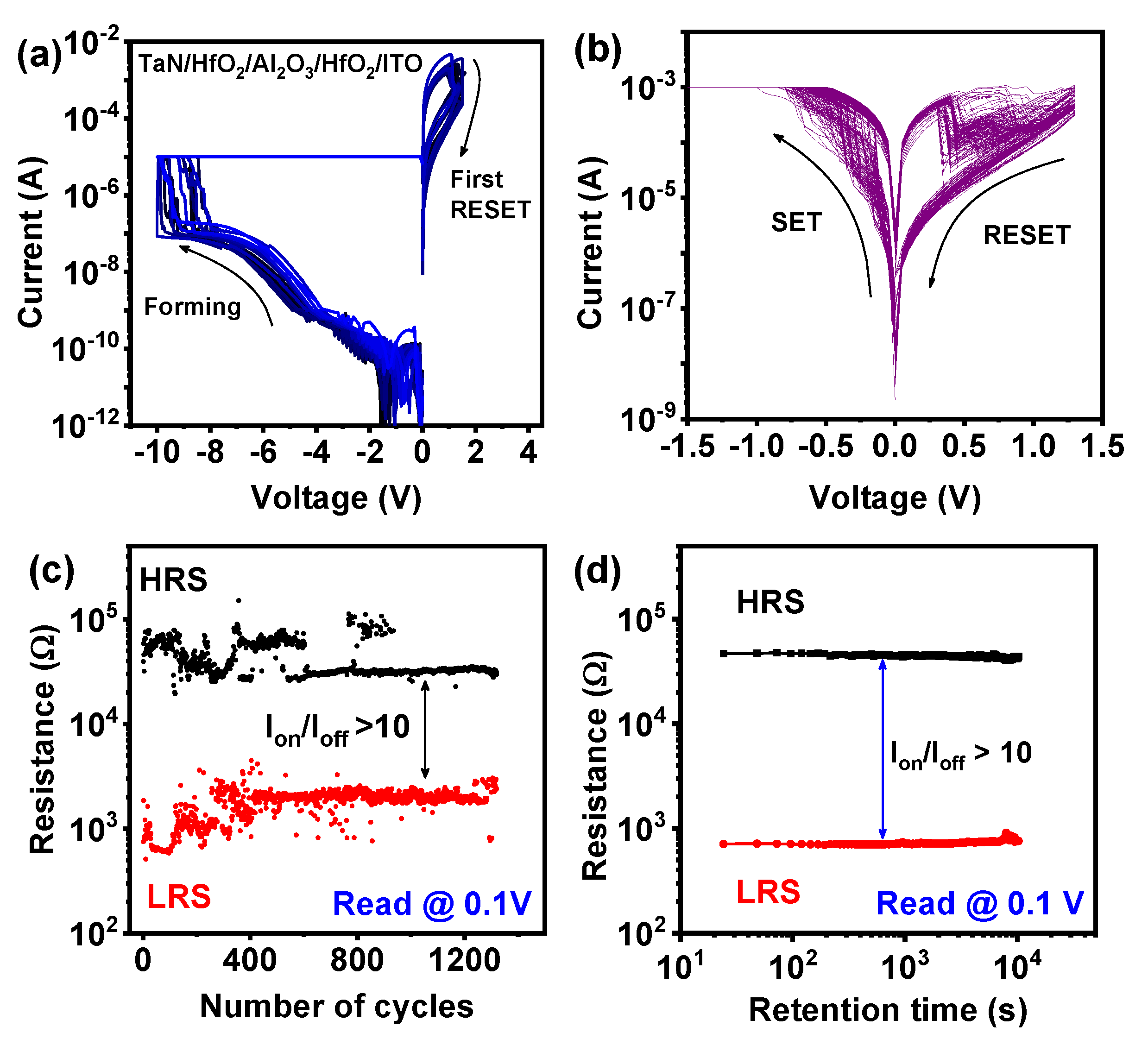
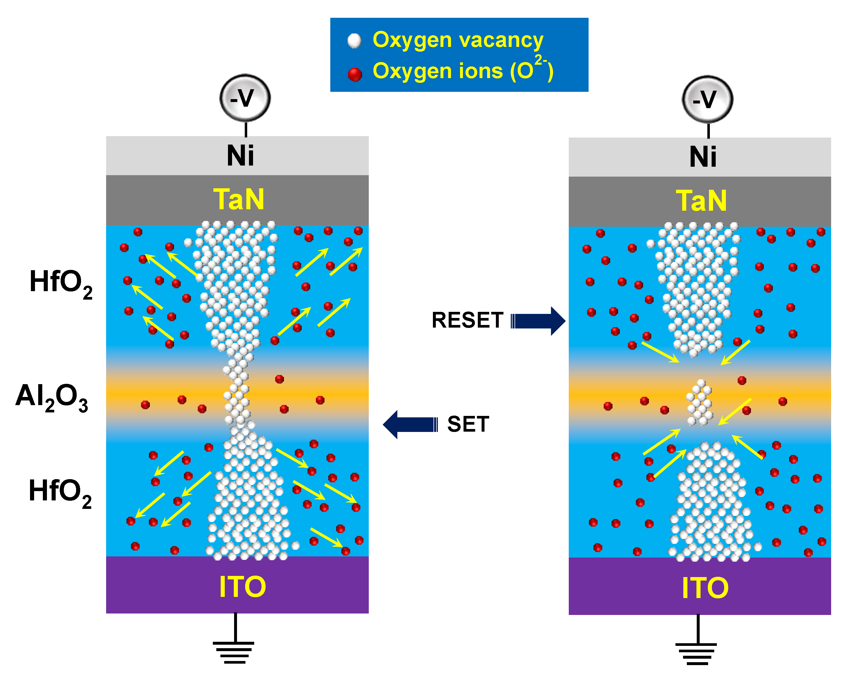
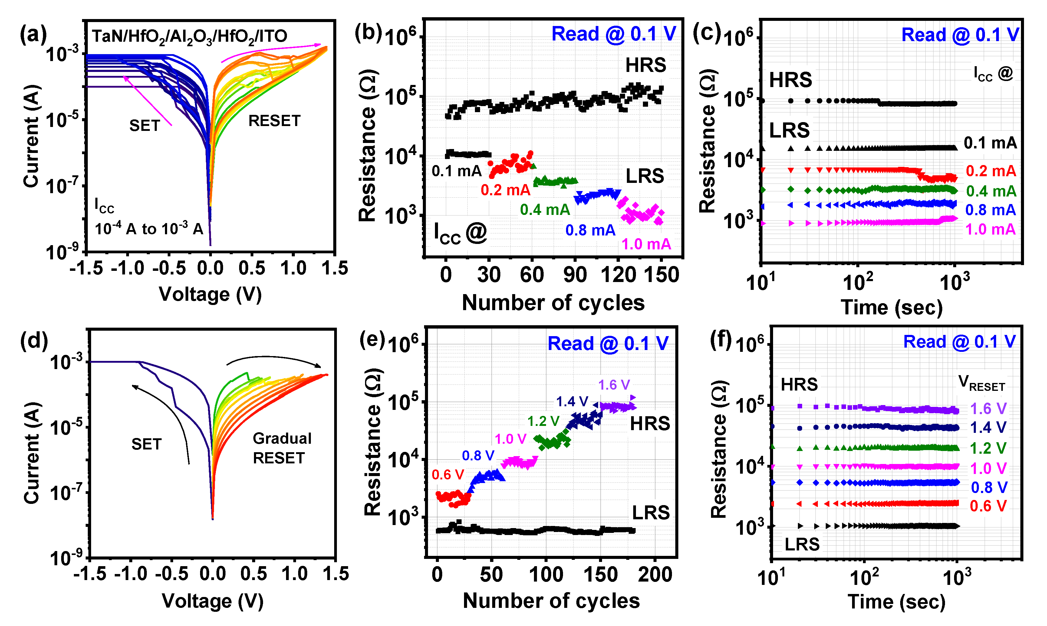
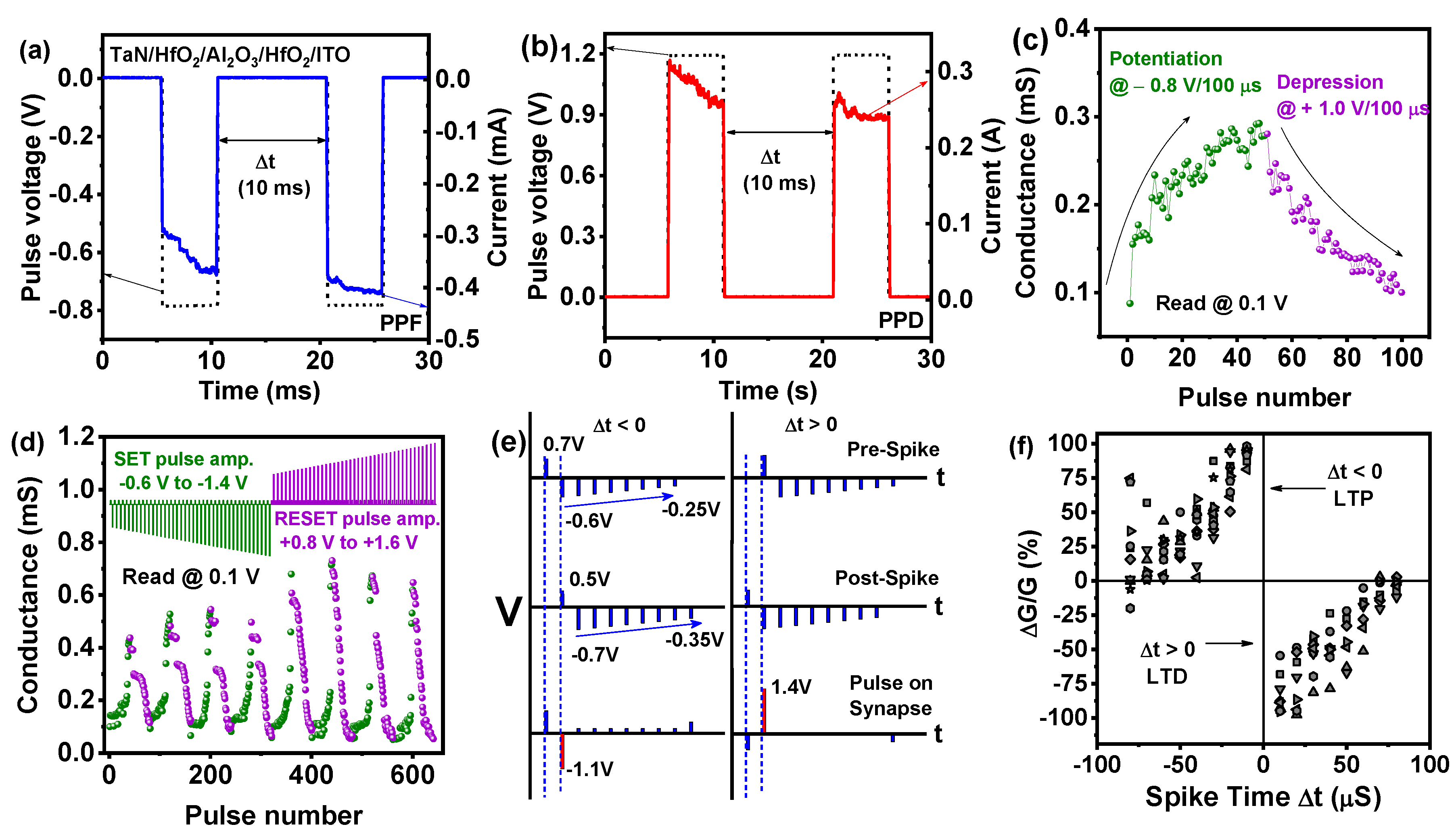
3. Results and Discussion

The cross-section of the TaN/HfO2/Al2O3/HfO2/ITO tri-layer RRAM structure was investigated by the high-resolution transmission electron microscopy (HRTEM) image and the energy-dispersive X-ray spectroscopy (EDS) compositional mapping as shown in Figure 2. The total thickness of the tri-layer was confirmed to be ~12 nm, which was similar to the target thickness, as shown in Figure 2a,b. Different Ta, Hf, Al, O, In, and Sn element mapping confirms the presence of multilayer structures as shown in Figure 2c. To confirm the tri-layer more clearly, X-ray intensities of the line profiles are presented in Figure 2d, which confirmed the presence of HfO2/Al2O3/HfO2 tri-layer without any significant diffusion of In and Sn, which is due to low temperature (150 °C) ALD technique. In addition, from HRTEM and EDS analysis the inter-diffusion at Al2O3/HfO2 can be seen by the presence of hump, which can produce HfAlO, as presented in Figure 2d. According to Lan et al., intrinsic trap sites related to oxygen vacancies can be created due to the inter-diffusion between HfO2 and Al2O3 [30]. This inter-diffusion creates oxygen vacancies due to the presence of HfAlO in thin gate stacks. At both interface regions, the trivalent Al into HfO2 distributes intrinsic oxygen vacancies (VO), which control the gradual resistive switching in the RRAM device discussed in the next section. Figure 3a shows the forming and first RESET characteristics of the TaN/HfO2/Al2O3/HfO2/ITO tri-layer RRAM device. The initial forming process shows the similar behavior of multiple devices for the I-V soft breakdown under negative voltage applied to the top TaN electrode where the initial current compliance was set to 10−5 A. During the electroforming process, the conductive filament forms between two electrodes, which consist of mainly oxygen vacancies (VO). Gradual SET/RESET bipolar switching properties were found after the electroforming process at the SET current compliance of 10−3 A. Gradual SET/RESET during resistive switching is the requirement for future synaptic device applications for neuromorphic computing [31]. During the SET process, VO regrowth inside both the interfacial layers of Al2O3/HfO2 helps gradual change occur in the current, as shown in Figure 2b. Here, both HfO2 layers act as a virtual electrode (as HfO2 contains more oxygen vacancy compared to Al2O3) and during the RESET process only interface filament is believed to rapture due to positive bias at the top electrode, which controls the resistive switching process stability and reliability [20]. A schematic resistive switching mechanism has been presented in Figure 4.
After applying a negative bias at the electrode, oxygen vacancies are piled up mainly near the interface driven by the external electric field. The virtual electrode (formed during electroforming process) at both ends within HfO2 helps to regrow the CF. During RESET process, the CF is not fully ruptured, and VO recombines with oxygen ions gradually due to the applied positive bias at the top electrode, as shown in Figure 4. According to previous studies, asymmetric CF forms inside two different dielectrics. This further leads to formation of the weakest CF at the interface of two different dielectrics [14,32]. Hence, the redox reaction due to the migration of oxygen ions dominates the RESET process near the interface of two dielectrics, as described, with the switching mechanism in Figure 4 [20,32].The endurance characteristics were obtained for the tri-layer RRAM device with up to 1300 cycles with Ion/Ioff ratio > 10, as shown in Figure 3c, read at 0.1 V. Initial variation of low resistance state (LRS) and high resistance state (HRS) can be due to the large area of the top electrode, where a large number of conductive filaments are created during the forming process. Data retention at a read voltage of 0.1 V, for LRS and HRS, was recorded up to 104 s without any significant variation, as shown in Figure 3d. To understand the performance of the proposed tri-layer RRAM device, a detailed comparison of electrical parameters is presented in Table 1.
Multi-level resistance states depending on the SET current compliance (Icc) were investigated to find the influence of increasing oxygen vacancy concentration inside conducting filaments (CF) [36,37,38]. Figure 5a shows the resistive switching characteristics with variable Icc during the SET process from 100 µA to 1 mA. From low to high Icc, the resistance of the device continuously decreased as shown in Figure 5a. For the endurance test of each LRS, 30 cycles of each resistance state were monitored. As evident from Figure 5b, HRS remains almost constant and multiple LRS was found to be with 10.54 kΩ, 6.08 kΩ, 3.57 kΩ, 2.13 kΩ, 1.01 kΩ at the read voltage of 0.1 V. The decrease in resistance can be explained by the increased width of CF inside tri-layer dielectric films, concerning the continuous enhancement of VO [36]. The stability of different resistance states was confirmed by the retention test, as shown in Figure 5c, where different LRS maintained up to 103 s without any significant variation. Modulation of a multi-level conduction state is a very essential aspect for the synaptic device to realize the high-density memory storage. To achieve multilevel memory states, gradual RESET has been controlled by Vreset-stop, as shown in Figure 5d. A similar approach has been shown in recent works on bilayer and tri-layer RRAM structures to obtain multi-state resistance by controlling Vreset-stop [21,33,39,40]. Here, the positive RESET voltage was slowly increased to get a gradual RESET process in the HfO2/Al2O3/HfO2 tri-layer RRAM device, which leads to multiple HRS.
As mentioned above, the filament dissolution increased continuously at both Al2O3/HfO2 interface under increasing positive top electrode bias, which further leads to changing the device’s resistance. The stability of different HRS was confirmed by endurance tests for 30 cycles of each Vreset-stop, as shown in Figure 5e. As shown in Figure 4e, LRS along with multiple HRS were obtained from the RESET I-V read at 0.1 V. Different average resistance states were found to be 2.26 kΩ, 5.02 kΩ, 9.07 kΩ, 20.5 kΩ, 47.2 kΩ, 87.3 kΩ at the RESET voltage of 0.6 V, 0.8 V, 1.0 V, 1.2 V, 1.4 V, 1.6 V, respectively. Data retention is another important property for different HRS stabilities and synaptic applications. Figure 5f shows the retention properties up to 103 s for distinct LRS and six HRS states for testing the reliability of multi-state resistance. From this above experiment, it was confirmed that the HfO2/Al2O3/HfO2 tri-layer is suitable for high storage and multi-level analog RRAM applications.
Along with gradual conductance change under DC voltage, modulation of resistance was also studied by a sequential paired pulse. Analogous to the bio-synapse, suitable paired pulse application can change the resistance of the RRAM devices with a short interval of time [41,42,43]. So, it is believed that synapse response is higher at the second pulse if a paired pulse is applied to the synapse [44]. Figure 6a,b show the pair-pulse fluctuation (PPF) and paired-pulse depression (PPD) characteristics for TaN/HfO2/Al2O3/HfO2/ITO memristor device. PPF and PPD responses are monitored after implementing paired pulse of −0.8 V/5 ms and +1.2 V/5 ms, respectively, with an interval of 10 ms, which is the short-term change in synaptic weight. In the case of PPF, an increase in current can be noticed at the response of the second pulse compared to the first pulse, which indicates the generation of VO. In the case of PPD, the opposite phenomenon took place, where the pulse current was found to be reduced due to recombination of oxygen vacancies and oxygen ions. Therefore, this result indicates that tri-layer RRAM can simulate the bio-synapse in real-time signals. Calculated average PPF and PPD was calculated to be ~10.2% and ~7.5%, respectively, from the equation,
PPF = (I2 − I1)/I1 × 100%
where I1 and I2 are the final currents recorded at each paired pulse [45].
Adjustable gradual conductance increase and decrease (potentiation/depression) are very essential for electronic synapse and have been studied in this section. The tri-layer RRAM device exhibits a gradual change in conductance after applying a constant amplitude pulse train of −0.8 V/100 µs and +1.0 V/100 µs for potentiation and depression, respectively, as shown in Figure 6c. A consecutive 50 cycles of negative pulses and 50 cycles of positive pulses were applied to achieve gradual conductance change, which is consistent with the DC gradual switching behavior discussed before. These properties indicate the synaptic plasticity in response to the pulse train, similar to the long-term potentiation (LTP), and long-term depression (LTD) in biological synapse [46]. This conductance change phenomenon is assumed to be dominated by the separation and recombination of oxygen vacancies (VO) and oxygen ions near both interfaces of HfO2/Al2O3 after applying different polarity pulse at the top electrode. During RESET, oxygen vacancies and oxygen ions recombine slowly and reduce the filament width at the weak filaments formed at both HfO2/Al2O3 due to the application of positive pulse train [25]. During the application of the negative pulse train, again gradually the weak filaments formed at both interfaces. To implement more accurately synaptic efficiency, of the tri-layer TaN/HfO2/Al2O3/HfO2/ITO memristor, negative pulse, and positive depression pulse with increasing amplitude were applied for potentiation and depression characteristics [47,48,49]. For potentiation and depression, increasing the pulse amplitude from −0.6 to −1.4 V, with a −0.05 V step, and 0.8 to 1.6 V, with a 0.05 V step, respectively, was applied to each tri-layer RRAM device. The applied pulse sequence is presented in Figure 6c, with a read voltage of 0.1 V. A clear gradual increase/decrease in conductance was observed during the long-term potentiation (LTP) and long-term depression (LTD) process, which is similar to the synaptic change in the biological synapse. The change in conductance was measured by the peak current obtained from the read pulse of 0.1 V as shown in Figure 6d. An almost gradual increase in conductance and a gradual decrease in conductance was observed during all 8 cycles. During potentiation at increasing negative pulse voltage to the top electrode oxygen ions were depleted mainly from the HfO2/Al2O3 interface and created weak CF. The opposite phenomenon occurs with positive increasing pulse voltage at the top electrode and gradually the CF at the HfO2/Al2O3 interface becomes narrow. Successful implementation of eight cycles of potentiation and depression is presented, which proves the reliability of the synaptic property of the tri-layer device. Slightly increasing conductance behavior at LTP can be due to the occurrence of new VO creation at the HfO2/Al2O3 interface.
To emulate the Hebbian learning of spiking neural networks (SNN), we focus on mimicking the spike-timing-dependent plasticity (STDP) learning rule in the tri-layer TaN/HfO2/Al2O3/HfO2/ITO memristor, having been employed to simulate synapse functionality [50]. This learning rule depends on the relative time difference (Δt) of a set of spikes related to the pre-synaptic and post-synaptic neurons [51]. Design of the pre-spike, post-spike and consequent effective pulse applied to the synapse for time-division multiplexing (TDM) approach are shown in Figure 6e. Using this pulse sequence, the obtained STDP characteristics for synaptic learning rules in the tri-layer RRAM device was employed using the TDM approach, as shown in Figure 6d [50]. Presynaptic spikes and postsynaptic spikes were included as +0.7, −0.6, −0.55, −0.5, −0.45, −0.4, −0.35, −0.3, and −0.25 V and +0.5, −0.7, −0.65, −0.6, −0.55, −0.5, −0.45, −0.4, and −0.35 V, respectively. Here, it is considered that when the pre-spike precedes the post-spike (Δt > 0), potentiation occurs, and in the opposite case when the post-spike precedes the pre-spike (Δt < 0) the device is depressed. Positive synaptic weight change is observed in the IInd quadrant when Δt increases from 0 to ‒100 µs, which indicates synaptic potentiation, and negative synaptic weight change observed in the IVth quadrant when Δt varies from 0 to 100 µs is described as synaptic depression. The change of synaptic weight can be described as follows:
Δ w = { A + e Δ t / τ + A e Δ t / τ Δ t > 0 Δ t < 0
where A+ and A are the synapse maximum weights at Δt = 0, and τ+ and τ are the broadening of the STDP window [48]. From Figure 6d, it can be found that the maximum change in synaptic weight [ΔW(ΔG/G) = (Gfin − Gmin)/Gmin] for positive Δt was 98.3% and for negative Δt was −94.8%, which is very symmetric for tri-layer RRAM device. These results further confirm the superiority of the stable and reliable synaptic characteristics of the TaN/HfO2/Al2O3/HfO2/ITO memristor device.

4. Conclusions

In summary, bipolar resistive switching behavior and synaptic properties of ALD deposited TaN/HfO2/Al2O3/HfO2/ITO memristor were studied in detail. Bipolar resistive switching with a gradual change in conductance was confirmed by DC I-V and pulse application. Uniform gradual resistive switching can be attributed to the formation of HfAlO in the interface of HfO2/Al2O3 in the tri-layer dielectric stack, where more than 103 cycles of endurance and 104 s of retention were achieved. Through applying different pulse sequences, short-term plasticity and symmetrical long-term plasticity were studied by PPF and potentiation/depression. Successful STDP behavior was achieved using the TDM method with conductance change from −94.8% to 98.3%. The above results for tri-layer RRAM predict a promising nonvolatile memory based synaptic device for the next generation. Although optimization of deposition parameters and thickness of the dielectric stacks are needed in the future.

Author Contributions

C.M. designed the experiment concept, conducted the electrical measurements, wrote the manuscript; M.K. writing—review and editing, funding acquisition, investigation; S.K. designed the experiment concept, writing—review and editing, and supervised the study. All authors have read and agreed to the published version of the manuscript.

Funding

This research was supported by National R&D Program through the National Research Foundation of Korea (NRF) funded by Ministry of Science and ICT (2020M3F3A2A01085755) and in part by Basic Science Research Program through the National Research Foundation of Korea (NRF) funded by the Ministry of Education (2018R1A6A1A03023788).

Conflicts of Interest

The authors declare that they have no competing interest.

References

  1. Shima, H.; Takano, F.; Akinaga, H.; Tamai, Y.; Inoue, I.H.; Takagi, H. Resistance switching in the metal deficient-type oxides: NiO and CoO. Appl. Phys. Lett. 2007, 91, 2005–2008. [Google Scholar] [CrossRef]
  2. Chandrasekaran, S.; Simanjuntak, F.M.; Saminathan, R.; Panda, D.; Tseng, T.Y. Improving linearity by introducing Al in HfO2 as a memristor synapse device. Nanotechnology 2019, 30, 445205. [Google Scholar] [CrossRef] [PubMed]
  3. Yan, X.; Xiao, Z.; Lu, C. Characteristic investigation of highly oriented Hf0.5Zr0.5O2 thin-film resistive memory devices. Appl. Phys. Lett. 2020, 116, 013506. [Google Scholar] [CrossRef]
  4. Chand, U.; Huang, K.-C.; Huang, C.-Y.; Tseng, T.-Y. Mechanism of Nonlinear Switching in HfO2-Based Crossbar RRAM With Inserting Large Bandgap Tunneling Barrier Layer. IEEE Trans. Electron Devices 2015, 62, 3665–3670. [Google Scholar] [CrossRef]
  5. Tan, T.; Du, Y.; Cao, A.; Sun, Y.; Zhang, H.; Zha, G. Resistive switching of the HfOX/HfO2 bilayer heterostructure and its transmission characteristics as a synapse. RSC Adv. 2018, 8, 41884–41891. [Google Scholar] [CrossRef] [Green Version]
  6. Waser, R.; Dittmann, R.; Staikov, C.; Szot, K. Redox-based resistive switching memories nanoionic mechanisms, prospects, and challenges. Adv. Mater. 2009, 21, 2632–2663. [Google Scholar] [CrossRef]
  7. Conti, D.; Laurenti, M.; Porro, S.; Giovinazzo, C.; Bianco, S.; Fra, V.; Chiolerio, A.; Pirri, C.F.; Milano, G.; Ricciardi, C. Resistive switching in sub-micrometric ZnO polycrystalline films. Nanotechnology 2019, 30, 065707. [Google Scholar] [CrossRef]
  8. Woo, J.; Moon, K.; Song, J.; Kwak, M.; Park, J.; Hwang, H. Optimized Programming Scheme Enabling Linear Potentiation in Filamentary HfO2 RRAM Synapse for Neuromorphic Systems. IEEE Trans. Electron Devices 2016, 63, 5064–5067. [Google Scholar] [CrossRef]
  9. Parreira, P.; Paterson, G.W.; McVitie, S.; MacLaren, D.A. Stability, bistability and instability of amorphous ZrO2 resistive memory devices. J. Phys. D Appl. Phys. 2016, 49, 095111. [Google Scholar] [CrossRef]
  10. Bousoulas, P.; Michelakaki, I.; Skotadis, E.; Tsigkourakos, M.; Tsoukalas, D. Low-Power Forming Free TiO2–x/HfO2–y/TiO2–x-Trilayer RRAM Devices Exhibiting Synaptic Property Characteristics. IEEE Trans. Electron Devices 2017, 64, 3151–3158. [Google Scholar] [CrossRef]
  11. Zhang, W.; Kong, J.-Z.; Cao, Z.-Y.; Li, A.-D.; Wang, L.-G.; Zhu, L.; Li, X.; Cao, Y.-Q.; Wu, D. Bipolar Resistive Switching Characteristics of HfO2/TiO2/HfO2 Trilayer-Structure RRAM Devices on Pt and TiN-Coated Substrates Fabricated by Atomic Layer Deposition. Nanoscale Res. Lett. 2017, 12, 393. [Google Scholar] [CrossRef] [PubMed]
  12. Chen, L.; Dai, Y.-W.; Sun, Q.-Q.; Guo, J.-J.; Zhou, P.; Zhang, D.W. Al2O3/HfO2 functional stack films based resistive switching memories with controlled SET and RESET voltages. Solid State Ionics 2015, 273, 66–69. [Google Scholar] [CrossRef]
  13. Wang, R.; Shi, T.; Zhang, X.; Wang, W.; Wei, J.; Lu, J.; Zhao, X.; Wu, Z.; Cao, R.; Long, S.; et al. Bipolar Analog Memristors as artificial synapses for neuromorphic computing. Materials 2018, 11, 2102. [Google Scholar] [CrossRef] [PubMed] [Green Version]
  14. Huang, C.Y.; Huang, C.Y.; Tsai, T.L.; Lin, C.A.; Tseng, T.Y. Switching mechanism of double forming process phenomenon in ZrOx/HfOy bilayer resistive switching memory structure with large endurance. Appl. Phys. Lett. 2014, 104, 2–6. [Google Scholar] [CrossRef] [Green Version]
  15. Banerjee, W.; Zhang, X.; Luo, Q.; Lv, H.; Liu, Q.; Long, S.; Liu, M. Design of CMOS Compatible, High-Speed, Highly-Stable Complementary Switching with Multilevel Operation in 3D Vertically Stacked Novel HfO2/Al2O3/TiOx (HAT) RRAM. Adv. Electron. Mater. 2018, 4, 1700561. [Google Scholar] [CrossRef]
  16. Ismail, M.; Abbas, H.; Choi, C.; Kim, S. Stabilized and RESET-voltage controlled multi-level switching characteristics in ZrO2-based memristors by inserting a-ZTO interface layer. J. Alloys Compd. 2020, 835, 155256. [Google Scholar] [CrossRef]
  17. Ding, X.; Feng, Y.; Huang, P.; Liu, L.; Kang, J. Low-Power Resistive Switching Characteristic in HfO2/TiOx Bi-Layer Resistive Random-Access Memory. Nanoscale Res. Lett. 2019, 14, 157. [Google Scholar] [CrossRef] [Green Version]
  18. Song, W.; Wang, W.; Lee, H.K.; Li, M.; Zhuo, V.Y.-Q.; Chen, Z.; Chui, K.J.; Liu, J.-C.; Wang, I.-T.; Zhu, Y.; et al. Analog switching characteristics in TiW/Al2O3/Ta2O5/Ta RRAM devices. Appl. Phys. Lett. 2019, 115, 133501. [Google Scholar] [CrossRef]
  19. Jeon, H.; Park, J.; Jang, W.; Kim, H.; Ahn, S.; Jeon, K.J.; Seo, H.; Jeon, H. Detection of oxygen ion drift in Pt/Al2O3/TiO2/Pt RRAM using interface-free single-layer graphene electrodes. Carbon 2014, 75, 209–216. [Google Scholar] [CrossRef]
  20. Wang, L.G.; Qian, X.; Cao, Y.Q.; Cao, Z.Y.; Fang, G.Y.; Li, A.D.; Wu, D. Excellent resistive switching properties of atomic layer-deposited Al2O3/HfO2/Al2O3 trilayer structures for non-volatile memory applications. Nanoscale Res. Lett. 2015, 10, 1–8. [Google Scholar] [CrossRef] [Green Version]
  21. Liu, J.; Yang, H.; Ma, Z.; Chen, K.; Zhang, X.; Huang, X.; Oda, S. Characteristics of multilevel storage and switching dynamics in resistive switching cell of Al2O3/HfO2/Al2O3 sandwich structure. J. Phys. D Appl. Phys. 2018, 51, 025102. [Google Scholar] [CrossRef]
  22. Maestro-Izquierdo, M.; Gonzalez, M.B.; Jimenez-Molinos, F.; Moreno, E.; Roldan, J.B.; Campabadal, F. Unipolar resistive switching behavior in Al2O3/HfO2 multilayer dielectric stacks: Fabrication, characterization and simulation. Nanotechnology 2020, 31, 135202. [Google Scholar] [CrossRef]
  23. Cazorla, M.; Aldana, S.; Maestro, M.; González, M.B.; Campabadal, F.; Moreno, E.; Jiménez-Molinos, F.; Roldán, J.B. Thermal study of multilayer resistive random access memories based on HfO2 and Al2O3 oxides. J. Vac. Sci. Technol. B 2019, 37, 012204. [Google Scholar] [CrossRef]
  24. Huang, R.; Yan, X.; Ye, S.; Kashtiban, R.; Beanland, R.; Morgan, K.A.; Charlton, M.D.B.; de Groot, C.H. Compliance-free ZrO2/ZrO2—x/ZrO2 resistive memory with controllable interfacial multistate switching behaviour. Nanoscale Res. Lett. 2017, 12, 384. [Google Scholar] [CrossRef] [PubMed] [Green Version]
  25. Moon, K.; Lim, S.; Park, J.; Sung, C.; Oh, S.; Woo, J.; Lee, J.; Hwang, H. RRAM-based synapse devices for neuromorphic systems. Faraday Discuss. 2019, 213, 421–451. [Google Scholar] [CrossRef] [PubMed]
  26. Zhang, R.; Huang, H.; Xia, Q.; Ye, C.; Wei, X.; Wang, J.; Zhang, L.; Zhu, L.Q. Role of Oxygen Vacancies at the TiO2/HfO2 Interface in Flexible Oxide-Based Resistive Switching Memory. Adv. Electron. Mater. 2019, 5, 1–7. [Google Scholar] [CrossRef]
  27. Shih, C.C.; Chang, K.C.; Chang, T.C.; Tsai, T.M.; Zhang, R.; Chen, J.H.; Chen, K.H.; Young, T.F.; Chen, H.L.; Lou, J.C.; et al. Resistive switching modification by ultraviolet illumination in transparent electrode resistive random access memory. IEEE Electron Device Lett. 2014, 35, 633–635. [Google Scholar] [CrossRef]
  28. Ye, C.; Wu, J.J.; Pan, C.H.; Tsai, T.M.; Chang, K.C.; Wu, H.; Deng, N.; Qian, H. Boosting the performance of resistive switching memory with a transparent ITO electrode using supercritical fluid nitridation. RSC Adv. 2017, 7, 11585–11590. [Google Scholar] [CrossRef] [Green Version]
  29. Kim, H.D.; Yun, M.J.; Kim, S. All ITO-based transparent resistive switching random access memory using oxygen doping method. J. Alloys Compd. 2015, 653, 534–538. [Google Scholar] [CrossRef]
  30. Lan, X.; Ou, X.; Lei, Y.; Gong, C.; Yin, Q.; Xu, B.; Xia, Y.; Yin, J.; Liu, Z. The interface inter-diffusion induced enhancement of the charge-trapping capability in HfO2/Al2O3 multilayered memory devices. Appl. Phys. Lett. 2013, 103, 192905. [Google Scholar] [CrossRef]
  31. Yu, S.; Gao, B.; Fang, Z.; Yu, H.; Kang, J.; Wong, H.-S.P. A Low Energy Oxide-Based Electronic Synaptic Device for Neuromorphic Visual Systems with Tolerance to Device Variation. Adv. Mater. 2013, 25, 1774–1779. [Google Scholar] [CrossRef] [PubMed]
  32. Tsai, T.L.; Chang, H.Y.; Lou, J.J.C.; Tseng, T.Y. A high performance transparent resistive switching memory made from ZrO2/AlON bilayer structure. Appl. Phys. Lett. 2016, 108, 2–6. [Google Scholar] [CrossRef]
  33. Akbari, M.; Kim, M.-K.; Kim, D.; Lee, J.-S. Reproducible and reliable resistive switching behaviors of AlOX/HfOX bilayer structures with Al electrode by atomic layer deposition. RSC Adv. 2017, 7, 16704–16708. [Google Scholar] [CrossRef] [Green Version]
  34. Huang, C.Y.; Jieng, J.H.; Jang, W.Y.; Lin, C.H.; Tseng, T.Y. Improved resistive switching characteristics by Al2O3 layers inclusion in HfO2-based RRAM devices. ECS Solid State Lett. 2013, 2, 2013–2015. [Google Scholar] [CrossRef]
  35. Deuermeier, J.; Kiazadeh, A.; Klein, A.; Martins, R.; Fortunato, E. Multi-Level Cell Properties of a Bilayer Cu2O/Al2O3 Resistive Switching Device. Nanomaterials 2019, 9, 289. [Google Scholar] [CrossRef] [Green Version]
  36. Zahoor, F.; Azni Zulkifli, T.Z.; Khanday, F.A. Resistive Random Access Memory (RRAM): An Overview of Materials, Switching Mechanism, Performance, Multilevel Cell (mlc) Storage, Modeling, and Applications. Nanoscale Res. Lett. 2020, 15, 90. [Google Scholar] [CrossRef]
  37. Misha, S.H.; Tamanna, N.; Woo, J.; Lee, S.; Song, J.; Park, J.; Lim, S.; Park, J.; Hwang, H. Effect of Nitrogen Doping on Variability of TaOx -RRAM for Low-Power 3-Bit MLC Applications. ECS Solid State Lett. 2015, 4, P25–P28. [Google Scholar] [CrossRef] [Green Version]
  38. Wu, L.; Liu, H.; Li, J.; Wang, S.; Wang, X. A Multi-level Memristor Based on Al-Doped HfO2 Thin Film. Nanoscale Res. Lett. 2019, 14, 177. [Google Scholar] [CrossRef] [Green Version]
  39. Giovinazzo, C.; Sandrini, J.; Shahrabi, E.; Celik, O.T.; Leblebici, Y.; Ricciardi, C. Analog Control of Retainable Resistance Multistates in HfO2 Resistive-Switching Random Access Memories (ReRAMs). ACS Appl. Electron. Mater. 2019, 1, 900–909. [Google Scholar] [CrossRef]
  40. Lin, S.M.; Tseng, J.Y.; Su, T.Y.; Shih, Y.C.; Huang, J.S.; Huang, C.H.; Lin, S.J.; Chueh, Y.L. Tunable multilevel storage of complementary resistive switching on single-step formation of ZnO/ZnWOx bilayer structure via interfacial engineering. ACS Appl. Mater. Interfaces 2014, 6, 17686–17693. [Google Scholar] [CrossRef]
  41. Hu, S.G.; Liu, Y.; Chen, T.P.; Liu, Z.; Yu, Q.; Deng, L.J.; Yin, Y.; Hosaka, S. Emulating the paired-pulse facilitation of a biological synapse with a NiOx-based memristor. Appl. Phys. Lett. 2013, 102, 183510. [Google Scholar] [CrossRef]
  42. Majumdar, S.; Tan, H.; Qin, Q.H.; van Dijken, S. Energy-Efficient Organic Ferroelectric Tunnel Junction Memristors for Neuromorphic Computing. Adv. Electron. Mater. 2019, 5, 1800795. [Google Scholar] [CrossRef] [Green Version]
  43. Wang, T.; Meng, J.; He, Z.; Chen, L.; Zhu, H.; Sun, Q.; Ding, S.; Zhang, D.W. Atomic Layer Deposited Hf0.5Zr0.5O2-based Flexible Memristor with Short/Long-Term Synaptic Plasticity. Nanoscale Res. Lett. 2019, 14, 102. [Google Scholar] [CrossRef] [PubMed] [Green Version]
  44. Liu, D.; Jing, Q.; Cheng, H. Synaptic-functional and fully water-soluble transient memristor made from materials compatible with semiconductor technology. Jpn. J. Appl. Phys. 2019, 58, 60903. [Google Scholar] [CrossRef]
  45. Li, H.K.; Chen, T.P.; Liu, P.; Hu, S.G.; Liu, Y.; Zhang, Q.; Lee, P.S. A light-stimulated synaptic transistor with synaptic plasticity and memory functions based on InGaZnOx-Al2O3 thin film structure. J. Appl. Phys. 2016, 119, 244505. [Google Scholar] [CrossRef]
  46. Mahata, C.; Lee, C.; An, Y.; Kim, M.-H.; Bang, S.; Kim, C.S.; Ryu, J.-H.; Kim, S.; Kim, H.; Park, B.-G. Resistive switching and synaptic behaviors of an HfO2/Al2O3 stack on ITO for neuromorphic systems. J. Alloys Compd. 2020, 826, 154434. [Google Scholar] [CrossRef]
  47. Zhao, L.; Xu, J.; Shang, X.; Li, X.; Li, Q.; Li, S. Synaptic memory devices from CoO/Nb:SrTiO3 junction. R. Soc. Open Sci. 2019, 6, 181098. [Google Scholar] [CrossRef] [Green Version]
  48. Wang, Q.; Niu, G.; Roy, S.; Wang, Y.; Zhang, Y.; Wu, H.; Zhai, S.; Bai, W.; Shi, P.; Song, S.; et al. Interface-engineered reliable HfO2-based RRAM for synaptic simulation. J. Mater. Chem. C 2019, 7, 12682–12687. [Google Scholar] [CrossRef]
  49. Li, Y.; Zhong, Y.; Zhang, J.; Xu, L.; Wang, Q.; Sun, H.; Tong, H.; Cheng, X.; Miao, X. Activity-dependent synaptic plasticity of a chalcogenide electronic synapse for neuromorphic systems. Sci. Rep. 2014, 4, 4906. [Google Scholar] [CrossRef] [Green Version]
  50. Kim, J.; Cho, S.; Kim, T.; Pak, J.J. Mimicking Synaptic Behaviors with Cross-Point Structured TiOx/TiOy-Based Filamentary RRAM for Neuromorphic Applications. J. Electr. Eng. Technol. 2019, 14, 869–875. [Google Scholar] [CrossRef]
  51. Zhao, J.; Zhou, Z.; Zhang, Y.; Wang, J.; Zhang, L.; Li, X.; Zhao, M.; Wang, H.; Pei, Y.; Zhao, Q.; et al. An electronic synapse memristor device with conductance linearity using quantized conduction for neuroinspired computing. J. Mater. Chem. C 2019, 7, 1298–1306. [Google Scholar] [CrossRef]
Figure 1. Schematic of TaN/HfO2/Al2O3/HfO2/indium tin oxide (ITO) resistive random access memory (RRAM) device structure with top and a bottom electrode connected to Keithley 4200 SCS semiconductor parameter.
Nanomaterials 10 02069 g001
Figure 2. (a,b) Cross-sectional high-resolution transmission electron microscopy (HRTEM) image of TaN/HfO2/Al2O3/HfO2/ITO tri-layer RRAM structure; (c) EDS elemental mapping; (d) line profiles of Ta, Hf, Al, O, In, and Sn for the cross-section of the device.
Nanomaterials 10 02069 g002
Figure 3. (a) Multiple initial forming characteristics under negative applied voltage to the top electrode and first RESET under positive voltage of TaN/HfO2/Al2O3/HfO2/ITO tri-layer RRAM device; (b) consecutive bipolar resistive switching characteristics of 200 SET/RESET cycles; (c) endurance characteristics of tri-layer RRAM device for 1300 switching cycles at a read voltage of 0.1 V; (d) memory retention of HRS and LRS for 104 s with a read voltage of 0.1 V.
Nanomaterials 10 02069 g003
Figure 4. Schematic diagram of resistive switching mechanism of the TaN/HfO2/Al2O3/HfO2/ITO RRAM during the SET and RESET process.
Nanomaterials 10 02069 g004
Figure 5. (a) Multilevel storage of tri-layer RRAM device under varying SET compliance currents from 100 µA to 1 mA; (b) reliability test for data endurance (30 cycles); (c) retention characteristics (103 s) with the corresponding increasing SET Icc; (d) bipolar resistive switching with multilevel high resistance state under increasing RESET voltage for tri-layer memristor device; (e) multi-level endurance characteristics under different RESET voltages for 30 cycles each; (f) retention characteristics of LRS and multilevel HRS under different RESET Vstop for 103 s.
Nanomaterials 10 02069 g005
Figure 6. (a) Paired-pulsed facilitation and (b) paired-pulsed depression phenomenon of tri-layer TaN/HfO2/Al2O3/HfO2/ITO memristor device under pulse spikes of −0.8 V and +1.2 V, respectively, with a time interval of 10 ms; (c) pulse potentiation/depression cycle with constant pulse width of −0.8 V/100 µs and +1.0 V/100 µs, respectively, read at 0.1 V (50 pulses of potentiation and 50 pulses of depression). (d) Repetitive 8 cycles of gradual conductance modulation for consecutive potentiation and depression controlled by increasing step pulse and read at 0.1 V; (e) details of pre-pulse and post-pulse scheme design using time-division multiplexing (TDM) approach to realize spike-timing-dependent plasticity (STDP) properties; (f) STDP characteristics of tri-layer RRAM device shows relative synaptic weight (ΔW) change with respect to spiking timing (Δt).
Nanomaterials 10 02069 g006
Table 1. Comparison of electrical parameters for different RRAM structures.
RRAM StructureOperation ModeForming Voltage
(V)
HRS/LRS
Ratio
Endurance
(Cycles)
Retention
(s)
Icc
(A)
Vset
(V)
Vreset
(V)
Ref.
AlOX/HfOXBipolarNA10240010410−30.8−1.0[33]
ZrO2/HfO2Bipolar−410210710410−31.0−1.0[14]
Al2O3/HfO2BipolarNA>10500NA10−30.9−0.8[12]
HfxAlyOBipolar2.710210410410−30.6−0.5[34]
HfO2/Al2O3Bipolar5.210210410410−51.8−1.5[4]
Cu2O/Al2O3Bipolar−3.0102NANA10−4−1.71.0[35]
HfO2/TiOxBipolar3.7102104NA10−61.5−1.1[17]
TiO2−x/HfO2−y/TiO2−xBipolarNA102107105free5.0−5.0[10]
Al2O3/HfO2/Al2O3BipolarNA102105105free−1.01.5[21]
HfO2/TiO2/HfO2Bipolar−3.710220010410−3−1.01.5[11]
ZrO2/ZrO2−x/ZrO2BipolarNA>10100NAfree−5.06.0[24]
Al2O3/HfO2/Al2O3Bipolar−2.0>1010310410−2−1.01.25[20]
HfO2/Al2O3/HfO2Bipolar−9.0>10>10310410−3−0.30.8This work
Publisher’s Note: MDPI stays neutral with regard to jurisdictional claims in published maps and institutional affiliations.

