1. Introduction
The recent development of lab-on-chip applications has highlighted the need to implement electrodes on flexible and stretchable materials, such as Polydimethylsiloxane (PDMS) [
1,
2,
3]. This silicone is widely used for medical applications due to its unique properties. It is transparent, flexible, gas permeable, and easy to structure [
4]. One of the promising research directions for PDMS-based applications is Organ-on-chip [
5,
6]. It is a microfluidic platform with various channels used for cell culture purposes. The main advantage of such a platform over the classical approach using a Petri dish is the possibility to emulate a dynamic microfluidic environment in a well-controlled, reproducible, and reconfigurable manner [
7]. Thus, the human body’s relevant conditions can be mimicked. However, due to the miniature size of the compartments and the encapsulation of the system (access to the channels is possible only via tiny mm sized inlets and outlets at the chip edges), it is impossible to insert the necessary measurement equipment for a Petri dish or Boyden chamber, e.g., Electrical Resistance System. However, measurements of the physiological and biological parameters in the direct vicinity of the cells (in situ) are required to characterize tissue functionality and cells’ reactions, e.g., in the presence of drugs [
1]. Thus, the next disruptive research direction in Micro-Electro-Mechanical Systems (MEMS) is sensor integration into a microfluidic platform for cell culture [
8,
9,
10,
11]. In addition, it is of great interest to integrate various actuator functionalities, which can help to manipulate liquid or cells [
12].
Depending on which medical or biological question we address through the Organ-on-Chip application, we might need to vary in situ temperature, e.g., for inflammation modeling. Therefore, we need to heat parts of the structure locally and most efficiently. As mentioned previously, PDMS is the most common silicone used for the realization of Organ-on-Chip devices. It has several interesting properties related to thermal behavior, e.g., PDMS gas permeability is firmly temperature-dependent. This effect can be used in applications that can take advantage of varying permeability by heating the PDMS substrate. If a heating element, which is essentially an electrode with specific target resistance, is directly applied on the PDMS surface, one can heat PDMS locally with high efficiency.
It is possible to structure metal electrodes on flexible polymers, such as polycarbonate (PC) or polyester (PET), and several research groups have reported sensor fabrication on these materials. For example, Henry et al. [
13] have reported gold electrodes patterned onto polycarbonate substrates for Transepithelial Electrical Resistance (TEER) measurements in a combined PC/PET/PDMS Organ-on-chip structure. In the case of a pure PDMS-based realization, the metal electrodes must be patterned on flexible and stretchable silicone. This poses additional significant research challenges on micro-structuring, such as micro-cracks, delamination, and potential degradation of electromechanical behavior caused by mechanical deterioration [
14]. In addition, metal deposition by magnetron sputtering can cause wrinkles/grooves on the PDMS surface, which in turn are transferred to the adsorbed metal [
15]. This effect may be due to the thermo-mechanical expansion of the PDMS during the metal deposition process and its relaxation [
16]. The authors of [
17] deposited Molybdenum on elastic PDMS, showing that naturally created wrinkles’ wavelength increases linearly with the metal film thickness. Their results are in good agreement with the continuous elastic theory. A similar surface modification, but more controlled, can be achieved by pre-stretching PDMS. This method can enable electrode “self-healing” in case of mechanical movements. Thus, the authors of [
18] deposited Zn nano-film on the pre-stretched PDMS using a direct current magnetron sputtering.
Interestingly, the authors of [
19] describe wrinkles which appear only close to cracks of the metal film. They applied DC magnetron sputtering of iron on uncured and partially cured PDMS substrates on a glass bottom layer. The authors of [
20] created a tunable metal film thickness gradient to better understand the ordered wrinkling patterns. They observed coexisting branched stripes, herringbones, and labyrinths along the direction of thickness decrease and explained it using a non-linear wrinkling model. The authors also fabricated tailored wrinkles based on Cu and thin PDMS [
21]. Promising applications for tailored wrinkled soft metalized layers [
22,
23] include strain sensors [
24] and droplet motion devices [
25]. However, considering the published works, there is no clear and univocal understanding of the wrinkle formation mechanism and behavior of large-area freestanding metallized soft polymer layers. In addition, no studies have been conducted on the dependence of wrinkle creation on the stiffness of Polydimethylsiloxane.
Therefore, in this work, we report the fabrication methodology and thermo-electrical and thermo-mechanical behavior of the first-time realized Cr/Au thermo-electric structure on a thin freestanding Polydimethylsiloxane membrane. In addition, we developed meander-shaped elements with different wire lengths to achieve higher resistance values. In this work, we also report natural wrinkle formation during magnetron sputtering on soft layers with various thicknesses of 20 µm and 40 µm. Moreover, we present the temperature–current and resistance–current characteristics of the meanders on freestanding and fixated PDMS layers. To the best of our knowledge, we investigate and report for the first time the influence of the substrate hardness on the thermo-electric characteristics of the metal structures on it. Therefore, we explore the impact of the 10:1 and 10:4 mixing ratios of the PDMS’s base and curing agent on the meanders’ thermo-electrical characteristics. Additionally, this paper investigates the PDMS/Cr/Au interface regarding naturally created wrinkles and discusses the physical background of its formation. Last but not least, we report the mechanical deformation of the PDMS freestanding membrane and the meanders’ movement by applying DC current.
3. Results and Discussion
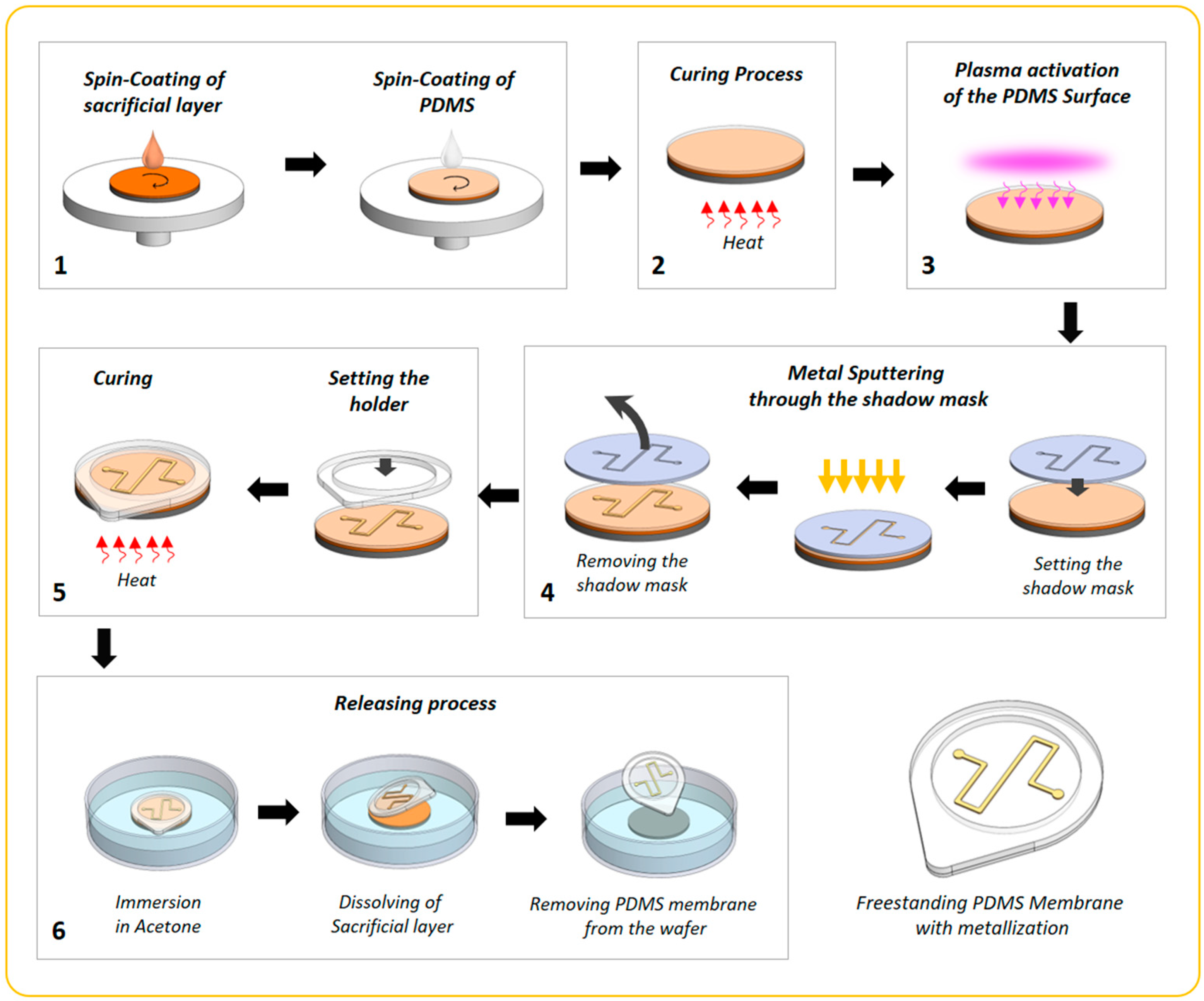
According to the processes described above (
Section 2.1), we have developed thermo-electric meander-shaped elements on a thin freestanding PDMS membrane. The samples described below were designed with the following intentions: PDMS membrane thickness was chosen to correspond to the one typically used in Organ-on-chip applications, which is in the range of 10 to 50 µm [
3,
5]; the geometric parameters of the thermo-electric element (wire width, length, and thickness) were set regarding the minimization of power consumption and ensuring power efficiency; and the mixing ratio of the PDMS was varied to improve the stiffness and handling of the thin membranes.
First, we characterized the surface of the initially cured PDMS layers to analyze and describe the developed structures.
Figure S3a shows it is smooth and replicates the substrate profile below. In our study, it is the silicon wafer with the spin-coated photoresist. As it occurs from our experience and in correlation with other works [
23], oxygen plasma treatment of PDMS makes its surface hydrophilic and improves the adhesion to metal. Therefore,
Figure S3b shows the PDMS surface after 20 s of oxygen plasma treatment. Even if wrinkles or deformations because of thermal expansion appeared during the plasma process at the blank PDMS layer, they must have vanished directly after it. Therefore, the surface shown is homogenous and planar. Moreover, the overall PDMS thickness variations were less than 2% of the respective membrane thickness. The precise values are given in
Table S1. In addition, the PDMS thickness inhomogeneity in the frame of each sample stays in the sub-micron level and is ±0.16 µm (
Table S2).
As shown in
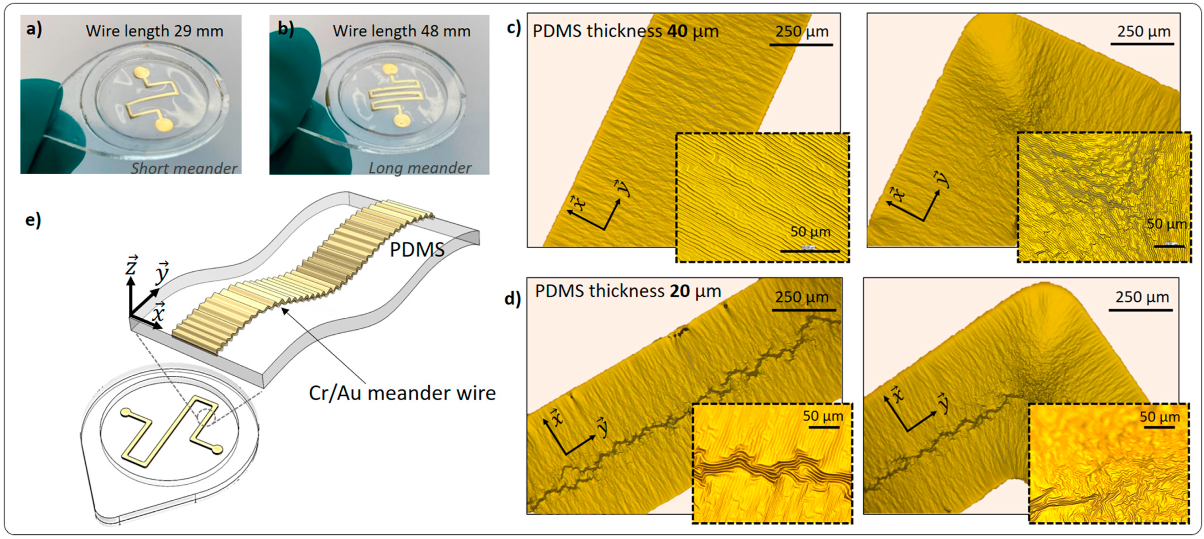
Figure 1, the next technological step is metal deposition. Hereof, we have sputtered the meander-shaped structures with 29 mm and 48 mm wire lengths through a shadow mask onto thin PDMS layers, shown in
Figure 2a,b, respectively. The resulting thickness of Cr, which is used as an adhesive layer, was 25 nm, and the resulting thickness of gold was 409 nm. The pull-off test shows a high adhesion rate of Cr/Au thin film to oxygen plasma-treated PDMS. The breaking strength value is 1.4 MPa.
After the magnetron sputtering, which is the argon plasma process, we observe wrinkled metal wires with one-directional (
) and two-directional deformations (
), as it is shown in
Figure 2c,d. The one-dimensional wrinkles were always induced parallel to the
direction with a wavelength λ of approximately 5 µm and amplitude
A of 0.27 µm (
Figure S5). In the corner of the meander, two directions are parallel to the wire width and converge. Therefore, two-directional wrinkles are formed. If a metal layer is deposited on PDMS, the polymer surface expands while being slightly heated. It should be noted that the overall temperature in the vacuum chamber does not exceed 30 °C, since we performed interval sputtering (
Section 2.1). We assume that the reason lies in the ejection of target metal atoms, which have sufficient kinetic energy to reach the substrate and disperse the rest of their energy, which is then converted into heat. Due to the heating that takes place on the surface of PDMS, a thermally induced mechanical expansion takes place. We observe this for the samples of 20 µm and 40 µm thickness. After cooling, the surface of PDMS—now with deposited metal on it—returns to its initial state, and wrinkles are formed. The result is coherent with the state of the art [
20,
21,
22,
23,
24,
25]. Therefore, the PDMS/metal wrinkles, shown in
Figure 2c,d, result from the plasma treatment which occurs in the course of sputtering. In our study, the wrinkles on metallized PDMS are formed naturally, without any pre-stretching of the PDMS.
Furthermore, in
Figure 2c,d, we compare the wrinkles on the wires sputtered onto 40 µm and 20 µm thick PDMS, respectively. In both cases, the thickness of the metal is identical. As it is seen in
Figure 2d, in the middle of the wire on 20 µm thick PDMS, a
prolonged wrinkle is present. However, this wrinkle cluster is absent on the 40 µm thick PDMS membranes. According to a theory in [
26], hierarchical wrinkles are generated due to the metal thickness gradient, which can appear at the metal deposition through the shadow mask. In our case, two metal thickness gradients are at opposite sides of the meander wire. Therefore, hierarchical wrinkles are created simultaneously from two opposite directions and meet in the middle of the wire. Then, the perpendicular grooves are formed due to the differences in wavelength, amplitude, and period of the two wrinkle clusters. However, this effect is not seen on the 40 µm PDMS membrane (
Figure 2c) and thicker membranes, e.g., 1 mm (
Figure S6). Obviously, the difference is due to the thickness of the soft substrate, but this parameter is not present in the wrinkling theory. In both the continuum elasticity theory [
20] and the non-linear wrinkling model [
26], the system is usually treated as a thin, rigid film resting on a semi-infinitely thick, compliant substrate under elastic deformation. Furthermore, the (
) labyrinth-like wrinkles are observed on the contact pad areas of the metal wire (
Figure S7), which have circular geometry with a diameter of 3 mm. The radial compression and isotropic thermal expansion of the PDMS resulted in hierarchical wrinkling over the entire circular area. Interestingly, the wrinkle pattern on the edge of the circle (
Figure S7a,b) is similar to the radial hierarchical wrinkle domains, obtained by the solvent evaporation method, presented in [
27]. At the same time, the middle part of the pad is filled with the labyrinth-like wrinkles, which are dependent on the elasticity of the substrate and deposited metal thickness, presented in several works [
17,
21,
27,
28]. Comparable wrinkling behavior was also observed on the sputtered without shadow mask circular thick samples (
Figure S8). The circular PDMS substrates of thickness from 0.1 mm to 1 mm with 0.1 mm step were entirely metalized and radial hierarchical wrinkling patterns were observed.
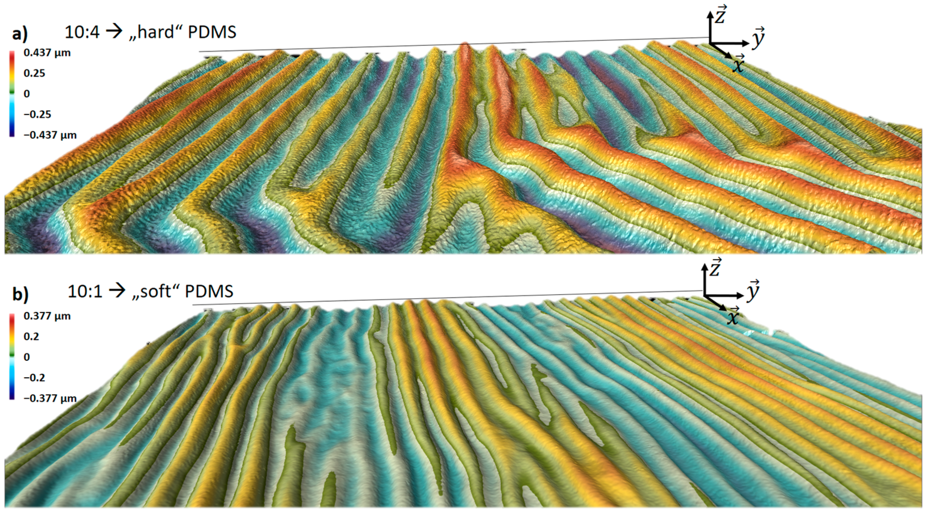
In the previous paragraph, we discovered the influence of the substrate geometry, but we also studied the influence of the PDMS material properties on metal wrinkling architecture. Accordingly, by manipulation of PDMS stiffness, we expected to increase its mechanical stability. Therefore, we fabricated identical samples to the previously described ones, but with the mixing ratio of 10:4 PDMS base and curing agent. It resulted in a PDMS hardness of 74.6 ± 0.1 HC, which is higher than that of samples with a mixing ratio of 10:1, with a hardness of 70.4 ± 0.1 HC. The surface, as expected, was partially flat without wrinkles (
Figure S9), but the wrinkled and non-wrinkled islands were irregularly alternated. Nevertheless, the wrinkled area of the PDMS/metal was dominating. Surprisingly, the wrinkles’ amplitude resulted in a higher value and was 0.437 µm for the 10:4 PDMS. Comparably, the average amplitude of the wrinkles on 10:1 PDMS was 0.26 µm. The roughness comparison of both PDMS types is shown in
Figure 3 and
Figure S7.
As described, wrinkles are generated by means of the PDMS thermo-mechanical expansion. Therefore, the entire meander wire is wrinkled (
Figure 2e), and its length is extended compared to the design parameters. Thus, a difference in calculated and measured meander resistance appears. The DC resistance of the shorter thermo-electric element, described in
Figure 3b, was measured to be approximately 11 Ω, while its calculated value is 3.5 Ω (factor of 3.14). Likewise, the calculated resistance of the longer device in
Figure 2b is 5.73 Ω, and its measured value is 14 Ω, which is 2.44 times higher due to the wrinkled structure of the wire. We estimate this tendency under the condition of unchanged wire thickness and width, as well as the resistivity of the metal.
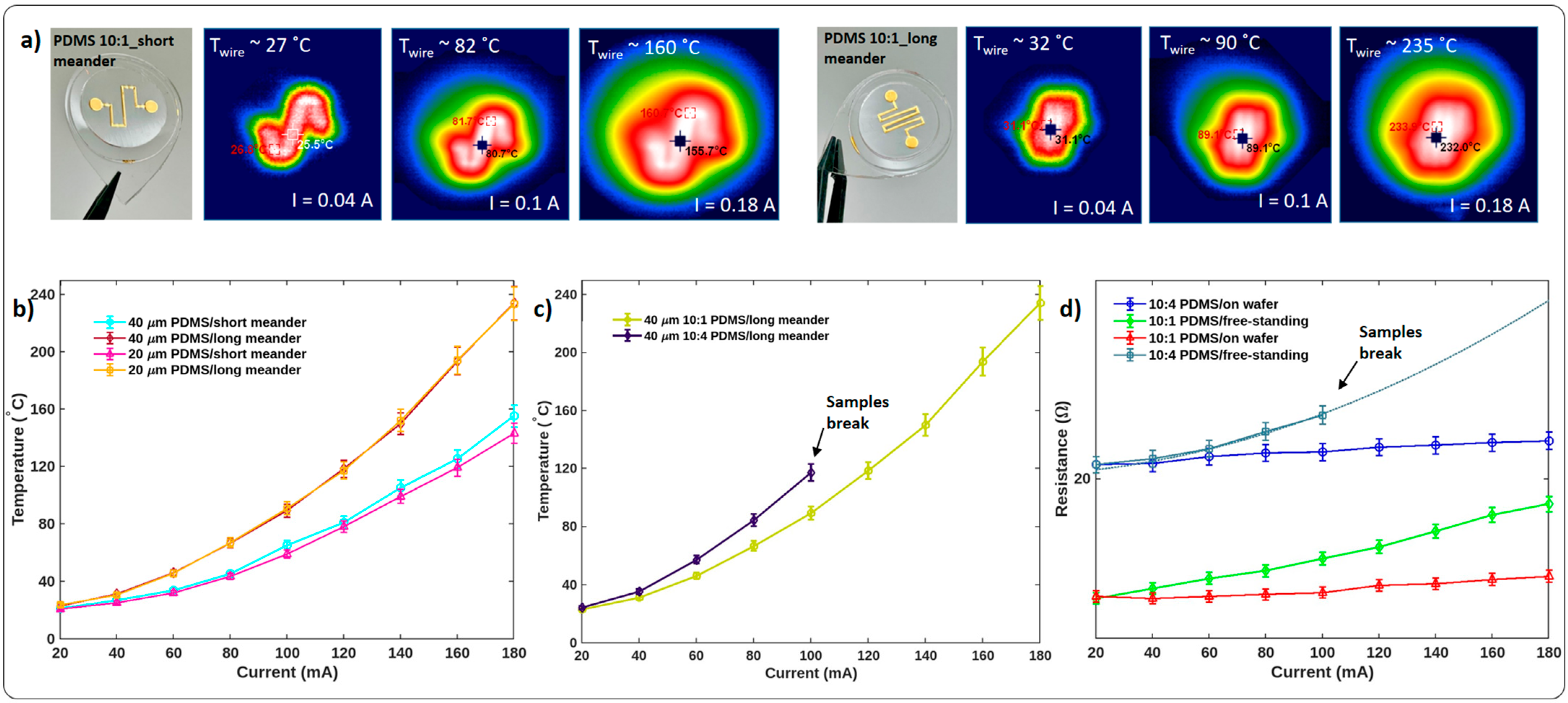
Figure 4a,b shows temperature measurements of the Cr/Au thermo-electric elements on 20 µm thin freestanding 10:1 PDMS membranes. At 180 mA, the wire temperature was approximately 160 °C for a short meander and 230 °C for the longer version. The temperature increases in a parabolic fashion, while the current growth corresponds to Joule’s first law. Consequently, due to the different resistances of short and long meanders, the slope of both classes of curves is also different. As we see in
Figure 4b, PDMS thickness does not affect the temperature behavior. However, the stiffness of the PDMS has an influence, as it is seen in
Figure 4c.
As mentioned previously and shown in
Figure 3, the wrinkle height of the 10:4 PDMS differs significantly from that of the 10:1 PDMS, by a factor of 1.68. Accordingly, the resistance of a meander of equal length sputtered onto hard PDMS is higher than that on soft PDMS. Therefore, the achieved temperature at the same applied current is significantly higher, as shown in
Figure 4c. The developed surface has a bigger area due to the wrinkles, as opposed to the purely planar case without wrinkles resulting in higher resistance. The resistance of the meander-shaped conductors realized on 10:4 PDMS is higher (20.7 Ω) than that of those realized on 10:1 PDMS (14.1 Ω). The resistance differs by a factor of 1.46. Thus, as shown in
Figure 4c, the temperature is also higher, so the change is proportional.
Furthermore, the resistance was measured while samples were located on the silicon wafer before releasing and in the freestanding condition after releasing.
Figure 4d shows that the presence of the silicon wafer does not influence the basic resistance, and curves start from the same resistance values. While applying current, we observe a different mechanical behavior of both membranes, since a freestanding membrane shows strong mechanical deflection, whereas a fixed membrane remains non-deformed. Thus, we must conclude that a thermally induced expansion/deflection takes place. The meanders’ and then the PDMSs’ temperature increases and resistance grows. The resistance of the freestanding 10:1 PDMS samples changes non-linearly and increases from 14.1 Ω to 18.7 Ω with applied current up to 180 mA (green line in
Figure 4d). The same but non-freestanding sample has less freedom to expand, and the heat is distributed into the silicon wafer underneath. Therefore, the resistance changes in a more linear manner and reaches 15.3 Ω at 180 mA (red line in
Figure 4d).
The same phenomenon is seen for the samples on hard 10:4 PDMS, with an initial basic resistance of 20.7 Ω. Hence, the thermo-electric elements on freestanding membranes reach 23.2 Ω at 100 mA, while the resistance of the sample on the wafer is 21.3 Ω at 100 mA (and 22.3 Ω at 180 mA). Nevertheless, freestanding samples with a 10:4 mixing ratio could not be measured at higher currents and temperatures because they tend to break. These samples had an inhomogeneous structure with alternating wrinkled and planar areas (
Figure S5). Therefore, microscopic cracks appear in the metal layer during the thermomechanical expansion of the PDMS, weakening the advantages of the wrinkled area. From this, a kind of self-healing effect of the metal layer in the area of the wrinkled substrate can be deduced, which is not so sensitive to thermally induced mechanical stresses. Interestingly, the resistance of the meanders on 10:1 PDMS and the wrinkles’ wavelengths, even after 60 on/off cycles, are reproducible. The resistance and wavelength values are given in
Table S3. According to the state of the art, the wrinkles provide a self-healing effect of the metal structure on the elastic substrate. However, this effect is not present in the samples with a 10:4 PDMS mixing ratio, and meander-shaped elements break (
Figure 4c) after a couple of loadings due to the generated cracks on the non-wrinkled islands (
Figure S9).
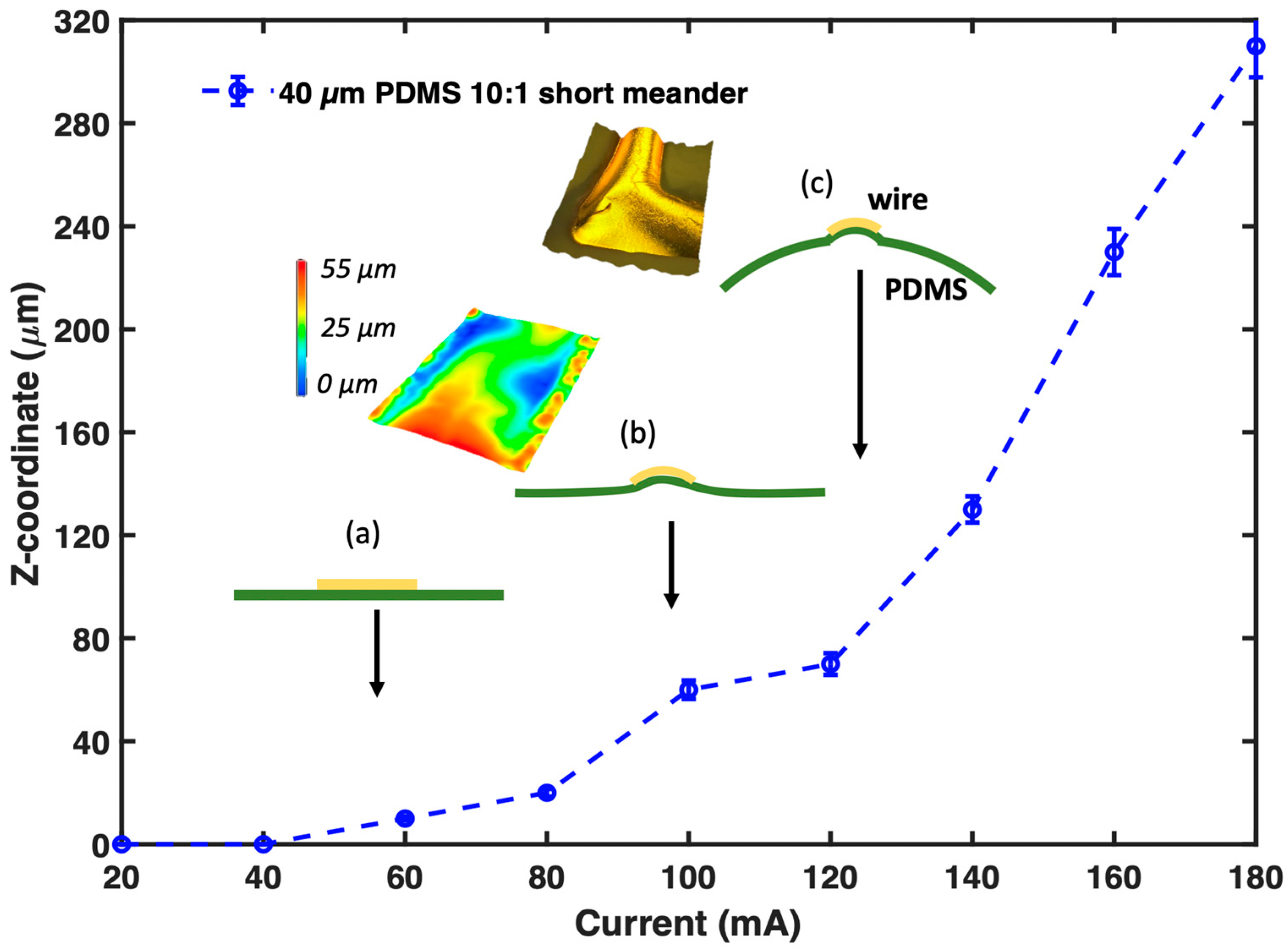
Moreover, in the course of the thermo-mechanical expansion, we observe an actuator behavior of the entire PDMS membrane equipped with a thermo-electric element. The topographic survey during heating is shown exemplarily for a freestanding 40 µm thick 10:1 PDMS membrane in
Figure 5. First, for the impressed DC current values ranging from 40 mA to 120 mA, we observe a mechanical movement of the wire (
Figure 5, insets (a) and (b)). It bulges starting from a planar structure in the region of the metalized surface. We attribute this effect to the temperature differences between the wire and the PDMS environment. The area with the metal on top starts to expand due to the fast heating. Thus, the wire bends in a spheroidal manner. The middle part of the wire slowly goes up. At the same time, PDMS without metal does not deform and holds the edges of the wire at the start position. Thus, the height difference reaches 70 µm (compare
z-coordinate of the diagram in
Figure 5). Then, with a further increase in current from 120 mA to 180 mA, we observe the bulging of the entire membrane while the wire remains bent (
Figure 5, inset (c)). The
Supplementary Video S1 also shows the described membrane’s overall motion. Notably, the wrinkles do not smooth while the wire bends and membrane bulges.
It should be mentioned that the samples on a 20 µm thin freestanding PDMS membrane show different motion behavior. The previously described prolonged wrinkle in the middle of the wire on 20 µm PDMS clearly influences the metal deformation: it buckles in the shape of a triangle, while the entire membrane continues to expand in the same curved shape as observed on the 40 µm PDMS membrane.
4. Conclusions
In summary, thermo-electric meander-shaped elements of 29 mm and 48 mm on freestanding 20 µm and 40 µm PDMS membranes were fabricated and analyzed. PDMS is a soft silicone-based polymer. Therefore, natural wrinkles appeared on the material during magnetron sputtering of Cr and Au. The metal preserves the grooves, ensures the metal structure’s conductivity, and provides a self-healing effect even if the substrate deforms. Therefore, the samples are stable, and the measurements are reproducible even after 60 cycles of heating and passive cooling.
Furthermore, we showed the influence of substrate thickness on wrinkle formation. Therefore, the 20 µm and 40 µm PDMS membranes with metal meanders were compared. On a 40 µm thick layer, the wrinkles were one-directional () except the meander corners, while on a 20 µm substrate, two-directional deformations () on the entire wire were present. According to the existing models, there are two clusters of hierarchical folds, with a directed deformation forming in the center of the wire due to the collision of the metal gradient on both sides of the wire and the wrinkles’ phase shift. Since the wrinkle patterns differentiate due to the PDMS thickness, it is necessary to consider this parameter in the future development of wrinkle formation theories.
In addition, due to the wrinkled substrate, the length of the wire is increased. Therefore, the measured blank resistance is 11 Ω, compared to its calculated value of 3.5 Ω for a short version of the meander of 29 mm. Additionally, the measured resistance of a 48 mm long wire is 14 Ω instead of the calculated resistance of 5.73 Ω.
Moreover, we investigated the PDMS mixing ratio’s influence on the thermo-electric meander-shaped elements. The amplitude of the wrinkles on the more rigid PDMS with a 10:4 mixing ratio is higher (0.437 µm) compared to the 10:1 PDMS membrane with an amplitude of 0.27 µm. As we described in our work, the wrinkles extend the effective wire length; therefore, the resistance and temperature of the wire on 10:4 PDMS are higher than on 10:1 PDMS at the same applied current. At the same time, wrinkles ensure the conductivity and stability of the wire. The samples on hard PDMS have inhomogeneity and planar areas, where µ-sized cracks appear at a current of 100 mA. These breaks and delamination are absent on 10:1 PDMS samples. Hence, we showed the “self-healing” effect of the wrinkled metal layer.
Additionally, we observed and described the thermo-mechanical movement behavior of the meander wires and complete PDMS membrane with a thermo-electric meander-shaped element, which deforms in a domed shape at an applied current of 120 mA. In its turn, the wire bending depends on the wrinkle shape and positioning. Subsequently, further investigation is needed to ensure the integration of the meander-shaped thermo-electric element on freestanding thin PDMS membranes as a sensor or actuator in lab-on-chip applications, since the resistance depends on the wrinkles formed during the manufacturing process and the thermo-mechanical movement during the operating process.


