Article

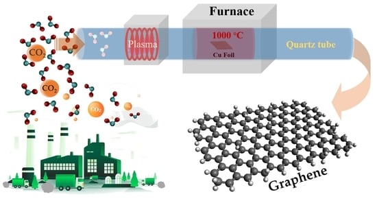
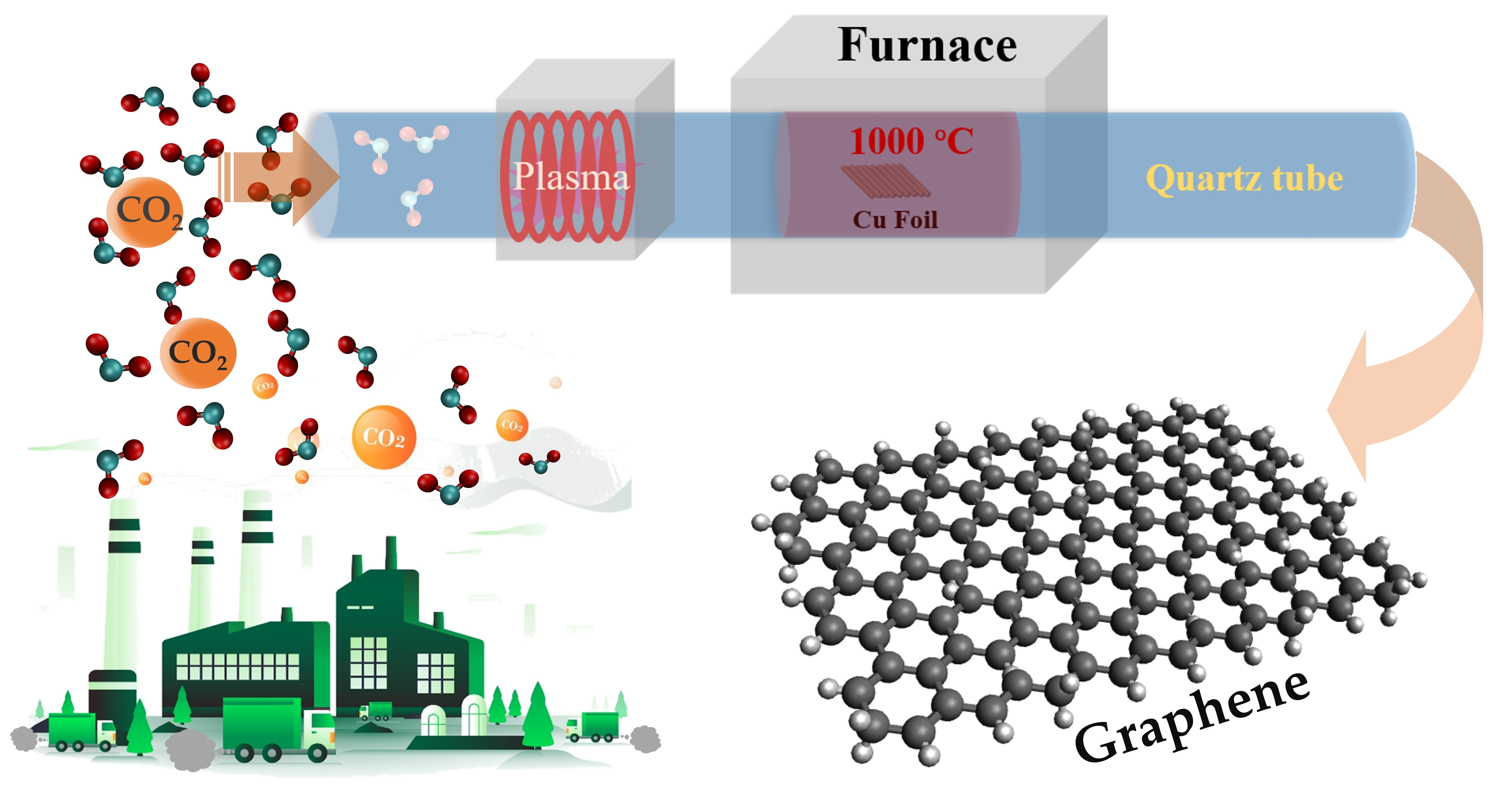
Conversion of Carbon Dioxide into Chemical Vapor Deposited Graphene with Controllable Number of Layers via Hydrogen Plasma Pre-Treatment

by
Yotsarayuth Seekaew
1,2,
Nantikan Tammanoon
1,
Adisorn Tuantranont
1,
Tanom Lomas
1,
Anurat Wisitsoraat
1,* and
Chatchawal Wongchoosuk
3,*
1
Graphene and Printed Electronics Research Division (GPERD), National Security and Dual-Use Technology Center, National Science and Technology Development Agency, 111 Thailand Science Park, Phahon Yothin Road, Klong Nueng, Klong Luang, Phathum Thani 12120, Thailand
2
Department of Physics, Faculty of Science, Ramkhamhaeng University, Bang Kapi, Bangkok 10240, Thailand
3
Department of Physics, Faculty of Science, Kasetsart University, Chatuchak, Bangkok 10900, Thailand
*
Authors to whom correspondence should be addressed.
Membranes 2022, 12(8), 796; https://doi.org/10.3390/membranes12080796
Submission received: 1 August 2022 / Revised: 14 August 2022 / Accepted: 16 August 2022 / Published: 18 August 2022
(This article belongs to the Collection Feature Papers in Membrane Surface and Interfaces)

Abstract

:
In this work, we report the conversion of carbon dioxide (CO2) gas into graphene on copper foil by using a thermal chemical vapor deposition (CVD) method assisted by hydrogen (H2) plasma pre-treatment. The synthesized graphene has been characterized by Raman spectroscopy, X-ray diffraction, scanning electron microscopy, and transmission electron microscopy. The results show the controllable number of layers (two to six layers) of high-quality graphene by adjusting H2 plasma pre-treatment powers (100–400 W). The number of layers is reduced with increasing H2 plasma pre-treatment powers due to the direct modification of metal catalyst surfaces. Bilayer graphene can be well grown with H2 plasma pre-treatment powers of 400 W while few-layer graphene has been successfully formed under H2 plasma pre-treatment powers ranging from 100 to 300 W. The formation mechanism is highlighted.

Graphical Abstract

1. Introduction

Carbon dioxide (CO2) is an important greenhouse gas in the atmosphere [1]. It helps to trap heat on our Earth’s surface and supports the growth of plants in the agricultural cycle [2,3]. However, high emission of CO2 produced by human activities, such as the combustion of fossil fuels to produce electricity, has recently caused serious problems in the form of global warming and climate change [4]. Moreover, exposure to atmospheric CO2 at high levels produces a variety of human health effects [5]. To mitigate the adverse effects of high CO2 emissions, there has been increasing research interest in CO2 reduction and utilization [6,7,8]. One of the most compelling utilizations of CO2 is to convert it into valuable products such as carbon-based nanomaterials, such as carbon quantum dots, inorganic nanoparticles, carbon nanotubes (CNTs) and graphene [9,10,11,12,13,14]. For examples, Kim et al. [15] synthesized the multi-walled CNTs by chemical vapor deposition (CVD) with NaBH4 reductant and NiCl2 catalyst. Ren et al. [16] demonstrated the preparation of carbon nanofibers via molten carbonate electrolysis from atmospheric CO2. Molina-Jirón et al. [17] reported the growth of graphene via atmospheric-pressure CVD with a catalytic Cu-Pd alloy. Licht et al. [18] produced carbon nanofibers and CNTs from CO2 using a solar thermal electrochemical process. Wang et al. [19] presented a transformation of CO2 into a carbon nano-scaffold by using electrolysis in molten carbonate. Until now, the development of new methods or technologies for the conversion of CO2 to valuable nanomaterials has been in great demand since CO2 emission has become one of the biggest global concerns, and as net zero by 2050 is the goal.
Graphene is one of the well-known two-dimensional (2D) materials that has exceptional physical, chemical, and electrical properties [20,21,22,23]. Currently, graphene has been widely applied in several applications including nanoelectronics, flexible electronics, batteries, super-capacitors, solar cells, gas sensors, membranes, and chemical sensors [11,24,25,26,27,28,29,30]. Graphene can be grown by numerous methods including CVD, mechanical exfoliation, chemical oxidation/reduction and electrolytic exfoliation [31,32,33]. Among them, CVD is one of the most popular graphene growth methods because it can produce a high-quality monolayer and few-layer graphene [34,35,36,37,38]. The basic principle of thermal CVD relies on the decomposition of gas molecules, such as methane [39], acetylene [40], ethylene [36], and ethanol [41], to react with some metal catalysts and induce graphene growth. Without metal catalysts on substrates, a high temperature of up to 1650 °C is required to overcome the large energy barrier for graphene nucleation [42].
In this work, we report the conversion of CO2 into graphene on copper foil substrates using a CVD method with hydrogen (H2) plasma pre-treatment. To our best knowledge, this is the first work to investigate the effects of H2 plasma pre-treatment to convert CO2 into graphene with the controllable few layers. Our finding demonstrates the important role of H2 plasma pre-treatment in the formation of few-layer graphene (two–six layers) by adjusting radio frequency (rf) powers for plasma pre-treatments (100–400 W).

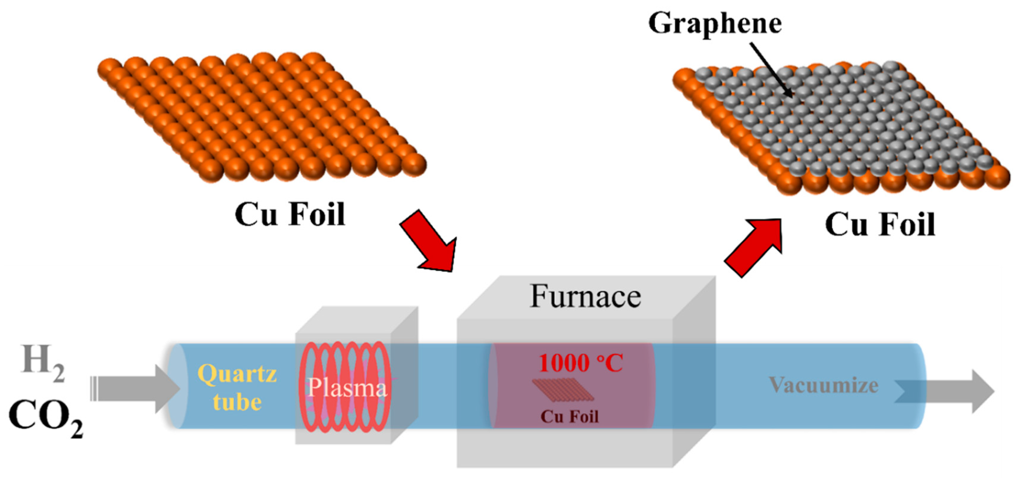
2. Materials and Methods

Copper (Cu) foil (25 µm thick, 99.98% metals basis) was purchased from Sigma-Aldrich Co., LLC, Darmstadt, Germany. The graphene was grown on the Cu foil by CVD method using CO2 gas (99.999% purity) as a carbon source, as shown in Figure 1. The growth process was conducted using a customized thermal CVD system integrated with an inductively coupled plasma system (planarGROW-4S, planarTECH LLC, The Woodlands, TX, USA). The distance from the plasma coil to the sample was ~75 cm. Before the Cu foil was loaded into a 4″ horizontal quartz tube of the CVD system, it was washed in ethanol solution for 10 min under ultrasonication and dried in air at room temperature. After the loading of samples, 150 sccm of H2 flowed into the CVD quartz tube while the reactor was heated to 1000 °C at a pressure of 1 Torr. At 1000 °C, the Cu foil surface was treated using H2 plasma generated by rf power for 30 min. The rf power was adjusted from 100 to 400 W in order to investigate the effects of H2 plasma pre-treatment. Next, a mixture of CO2 (50 sccm) and H2 (200 sccm) was applied at a working pressure of 2 Torr for 30 min for graphene growth on Cu foils. After the graphene growth stage, the CVD quartz tube reactor was cooled down to room temperature under an H2 flow of 150 sccm at 1 Torr. In the CVD process, the heating rate was set at 15 °C/min while the cooling rate was set at 10 °C/min. The graphene samples were characterized by field-emission scanning electron microscopy (FE-SEM: SU8030, Hitachi, Tokyo, Japan), X-ray diffraction (XRD: D8 Advance, Bruker, MA, USA), transmission electron microscopy (TEM: JEM-2100 Plus, JEOL, Tokyo, Japan), and Raman spectroscopy (InVia Raman Microscope, Renishaw, West Dundee, IL, USA) using a laser with an excitation wavelength of 785 nm.

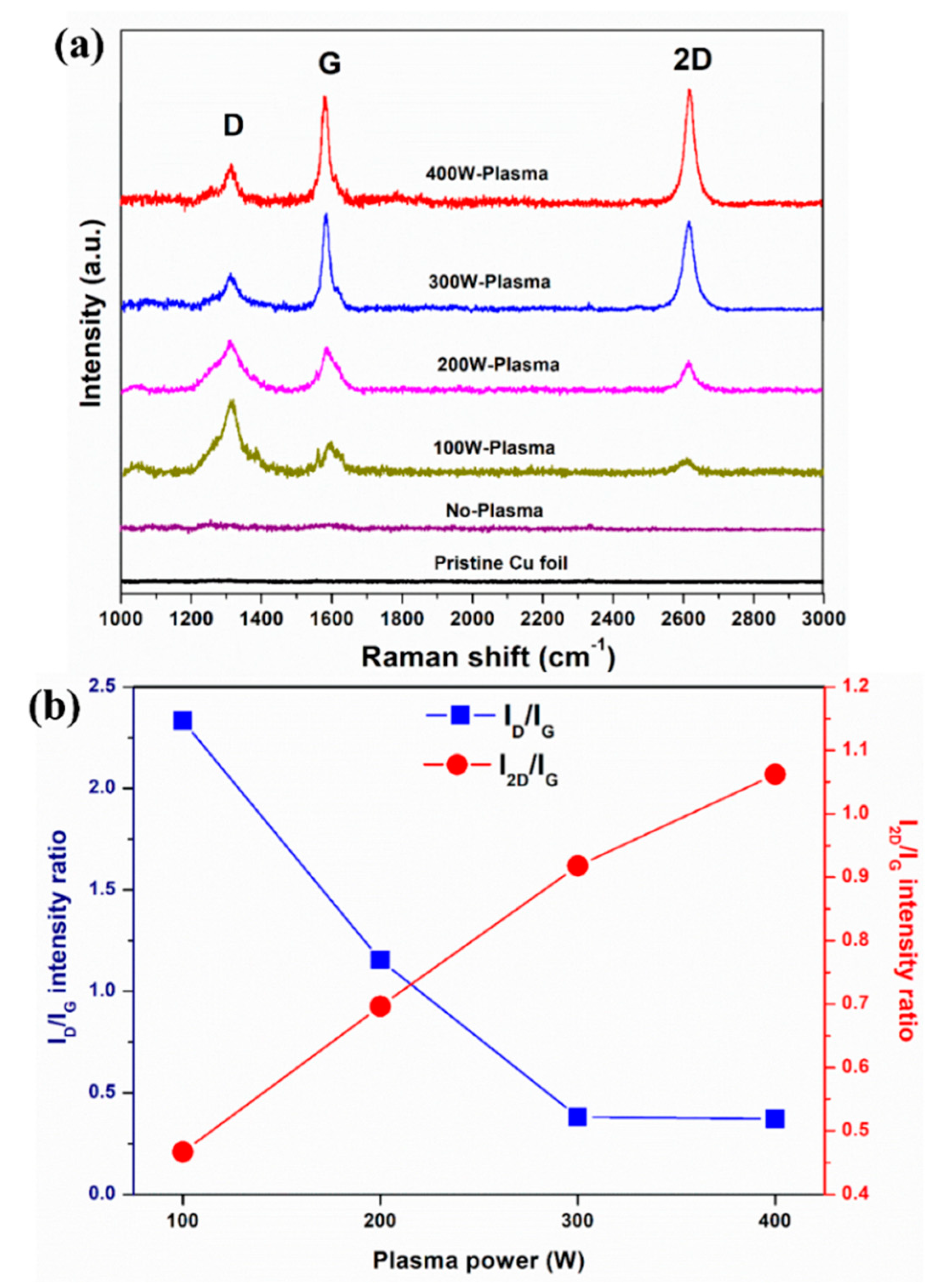
3. Results and Discussion

After the growth process, all samples were initially characterized by Raman spectroscopy as presented in Figure 2. It is evident that only the samples with H2 plasma pre-treatment (rf power = 100–400 W) exhibit D, G and 2D peaks at around 1300, 1580 and 2600 cm−1, respectively (Figure 2a). It is well known that the D peak is associated with lattice defects of the graphene structure while the G peak corresponds to primary sp2-hybridized carbon bonds in graphene. The 2D peak is the second order of the D band relating to one boundary defect in graphene [43,44]. Therefore, they confirm the formation of graphene on Cu surfaces with H2 plasma pre-treatments. At the same growth condition, no graphene was observed on Cu surfaces without H2 plasma pre-treatment. This indicates that the H2 plasma pre-treatment plays an important role in modifying the Cu surface for graphene nucleation.
To investigate the quality and number of graphene layers, the intensity ratios of the 2D to G band (I2D/IG) and D to G band (ID/IG) were calculated from the Raman spectra and are displayed in Figure 2b. The I2D/IG is known to be strongly related to the number of layers [34,45,46,47]. The I2D/IG > 2 indicates the monolayer graphene while 1 < I2D/IG < 2 and I2D/IG < 1 refer to the bilayer and trilayer/few-layer graphene, respectively. In Figure 2b, the I2D/IG increases from 0.47 to 1.06 with increasing rf plasma power from 100 W to 400 W, suggesting the formation of few-layer graphene and the decrease of the number of graphene layers to two on increasing the H2 plasma rf power to 400 W. Concerning the graphene quality, the ID/IG decreases from 2.33 to 0.37 as the rf plasma power increases from 100 W to 400 W. The decrease of the ID/IG intensity ratio implies the reduction of defect density. At the high plasma powers of 300–400 W, the ID/IG intensity ratio is as low as ~0.37, indicating graphene structures with low defect levels [48].
The graphene growth evolution with respect to the growth times, including 15, 30 and 45 min, using the rf plasma power of 400 W, is shown in Figure 3. At all reaction times, the grown surfaces exhibit three main Raman peaks (D, G and 2D), indicating that graphene has already formed at 15 min, with I2D/IG ~ 1 corresponding to the bilayer graphene structure. However, ID/IG (0.80) at 15 min is relatively high compared with ID/IG at 30 min (0.37) because the nucleated graphene is initially defective and these defects may be amended with additionally deposited atoms as the time progresses. For the extended growth time of 45 min, more layers of graphene are formed, leading to a significantly reduced I2D/IG in accordance with the previous reports of other CVD graphene growth studies using different times [49,50,51].
To evaluate the effects of H2 rf plasma power during pre-treatment on graphene growth, the XRD patterns of the pristine Cu foil and the graphene growth on Cu foils pre-treated with different H2 rf plasma powers are displayed in Figure 4. As seen in Figure 4a, all samples exhibit three pronounced peaks located at 43.34°, 50.46° and 74.16°, corresponding to Cu (111), Cu (200) and Cu (220) (JCPDS No. 65-9026), respectively [52,53]. Interestingly, Cu2O (111) phase at 37° [54,55] arises in comparison with pristine Cu (unheated) and samples with H2 plasma pre-treatments after the sample was heated to the growth temperature (1000 °C) in the CVD system (Figure 4b). The formation of Cu2O during the CVD process can suppress the graphene’s growth. With H2 plasma pre-treatments, Cu2O is absent and the C (002) peak at ~26° is detected, dictating the formation of graphene on Cu foil without other defect peaks in accordance with the Raman results, which indicate high quality graphene structures.
The detailed surface morphologies of graphene grown from CO2 on Cu foils pre-treated with varying H2 rf plasma powers are demonstrated in Figure 5. It clearly shows that the H2 plasma pre-treatment strongly affects the surface morphology of Cu foil. In this work, Cu foil acts as both catalyst and substrate. During the high-temperature CVD process, the recrystallization of Cu grain occurs and Cu2O is formed on the surface due to oxidation by residual oxygen. With H2 plasma pre-treatment, high rf powers can contribute to the removal of residual copper oxides on the surface as shown in Figure 5c–f. An increase of the rf plasma power results in a remarkable reduction in the density of residual oxides and enhances the carbon in-diffusion-controlled kinetics of CO2 flow in the reactor, leading to the formation of graphene. However, a large number of wrinkles are formed and some secondary nucleation always dominates. The wrinkles are caused by the discontinuous growth of monolayer graphene associated with the difference in thermal expansion between graphene and Cu [56,57]. Thus, only bilayer and few-layer graphene can be formed. In addition, the wrinkles of graphene on the Cu substrate are quite similar to the few-layer graphene wrinkles formed on other substrates such as Ni foam [58].
The number of layers of graphene grown on Cu foils pre-treated with different plasma powers was verified by high-resolution (HR) TEM images as displayed in Figure 6. The HR-TEM images clearly show graphene fringes displaying bilayer, trilayers, four layers, and six layers in accordance with the Raman results of graphene grown on Cu foils pre-treated with the plasma powers of 400, 300, 200 and 100 W, respectively. The thickness of graphene with bilayer, trilayers, four layers, and six layers is estimated to be ~0.69 nm, 1.18 nm, 1.64 nm and 2.50 nm, respectively. In addition, the interlayer spacing of graphene sheets can be determined to be ~0.35 nm in agreement with many other publications [17,59,60]. The selected area electron diffraction (SAED) pattern, as illustrated in the inset of Figure 6a, presents two sets of six-fold reflection spots of a hexagonal lattice. This evidence confirms the bilayer graphene structure with high quality [61].
The sheet resistances as a function of the rf plasma powers were also investigated as shown in Figure 7. The sheet resistance of graphene increases from ~75 to 100 Ω/sq on increasing the rf plasma power from 100 to 400 W. The number of graphene layers strongly correlates to band structure, energy gap, Fermi energy, and charge carriers, which directly affect the electrical conductivity [34,62,63,64]. From the characterization results, the number of graphene layers was six at 100 W and was reduced to two at 400 W. Both bilayer and multilayer graphene structures exhibit typical parabolic band structures associated with finite effective masses and charge carriers, which decrease with a decreasing number of graphene layers [34]. Bilayer graphene has more available electronic states in its valence band, leading to higher sheet resistances compared with multilayer graphene. In comparison with other substrates, the sheet resistance of graphene grown on Cu foil is smaller than that on PMMA and glass substrates (540–650 Ω/sq of bilayer and 300–350 Ω/sq of trilayer) [65,66]. The obtained low sheet resistance may be attributed to the uniformity of graphene film on the Cu surface and low defects compared with those produced by other methods [67]. To confirm the uniformity of graphene over the sample surface, FE-SEM images of bilayer graphene at five different regions on the Cu foil are displayed in Figure 8. It demonstrates that all regions show similar surface and wrinkle features of bilayer graphene on the Cu foil. Thus, the obtained bilayer graphene is highly uniform over the sample area.
The growth mechanism of CVD graphene depends on many factors, such as hydrocarbon gas source, pressure, flow rate, temperature, growth time, catalyst and substrate [68]. Several catalysts, such as Ni/Al2O3 [69], Cu-Pd [17], and NaCl–CaCl2–CaO [70], have been used to activate CO2 for the graphene growth. In this work, Cu foils act as both catalyst and substrate while only H2 plasma pre-treatment is used to activate the Cu catalyst with fixed temperature and time. Based on the characterization results, the H2 plasma power strongly affects the metal catalyst surface properties. Therefore, the formation of graphene with different numbers of layers is attributed to distinct metal catalyst surfaces pre-treated with different H2 plasma powers. In the synthesis step, CO2 is introduced as a carbon source for graphene growth. At high temperatures (~1000 °C), CO2 begins to decompose into carbon and oxygen atoms, generating CO and O [71], while CO2 can also directly react with H2 leading to the formation of H2O or other molecules (methane and methanol) [72,73]. The reaction for converting CO2 to graphene on the Cu surface can be described as CO2 + 2H2 → C + 2H2O [17]. However, copper oxide (Cu2O) formed on metal surfaces at high temperatures can suppress the diffusion of carbon species on the metal catalyst’s surface, preventing the nucleation of graphene. According to a previous study, graphene nucleation densities are low when Cu surfaces are relatively rough compared with the atomic thinness of the graphene [74]. From the results in this work, graphene cannot be formed without H2 plasma pre-treatment. The application of the H2 plasma pre-treatment on Cu foil can reduce residues on the surface and make the surface smoother. By increasing the H2 plasma power, residues are additionally removed, leading to an increasingly smooth Cu surface. The ingrained surface impurities act as nucleation sites for carbon adsorption during growth. Additional nucleation sites may be activated by H2 plasma pre-treatment to form the multilayer graphene. The H2 plasma power during pre-treatment can be thus used as a primary factor to control the number layers of graphene. In other words, C atoms dissociated from CO2 at a high growth temperature can diffuse the Cu surface into bulk to start the nucleation and growth of graphene on the catalyst’s surface. If the Cu surface confronts a contamination (oxidation of the unwanted impurities) before the precursor exposure, supersaturation of the surface is readily reached, limiting the nucleation of graphene. The H2 plasma pre-treatment can remove the contaminations on the catalyst surface and activate Cu active sites for graphene growth.

4. Conclusions

In conclusion, CO2 gas has successfully been converted into graphene films on Cu foils by way of a CVD method with H2 plasma pre-treatment. Raman spectroscopy, XRD, SEM, and TEM data demonstrate the formation of high-quality graphene with two–six layers on Cu foils. Without H2 plasma pre-treatment, a rough Cu surface with the cluster of oxide residues formed at a high growth temperature can suppress the diffusion of carbon species, resulting in no graphene nucleation. The introduction of the H2 plasma pre-treatment can remove residuals and enhance the CO2 flow kinetics on the Cu surface, assisting the nucleation and growth of graphene. The number of layers of graphene can be well controlled by varying the H2 plasma powers applied for the direct modification of metal catalyst surfaces before graphene growth. The proposed method requires no additional carrier gas and a catalyst for graphene growth from CO2. Therefore, it can be useful as an alternative way to convert CO2 greenhouse gas in the atmosphere into a valuable graphene film with a controllable number of layers.

Author Contributions

Conceptualization, Y.S. and A.W.; methodology, Y.S., N.T. and A.W.; validation, C.W.; formal analysis, Y.S., A.W. and C.W.; investigation, Y.S. and A.W.; resources A.T., T.L. and A.W.; data curation, Y.S. and N.T.; writing—original draft preparation, Y.S.; writing—review and editing, C.W. and A.W.; visualization, Y.S.; supervision, A.T., T.L. and A.W., funding acquisition, Y.S., A.W. and C.W. All authors have read and agreed to the published version of the manuscript.

Funding

This work was financially supported by Program Management Unit for National Competitiveness Enhancement (PMU-C), National Research Council of Thailand (N41A640126) and Kasetsart University Research and Development Institute (FF(KU) 25.64).

Institutional Review Board Statement

Not applicable.

Informed Consent Statement

Not applicable.

Data Availability Statement

The data presented in this study are available on request from the corresponding author.

Acknowledgments

The authors gratefully acknowledged the research funding in the project entitled, Synthesis of Graphene from Carbon Dioxide Waste for Industrial Applications (P2051414), from Program Management Unit for National Competitiveness Enhancement (PMU-C) and the Thailand Research Fund for TRF Research Team Promotion Grant (RTA6180004). The Research Grant for Talented Young Researchers (N41A640126) from National Research Council of Thailand (NRCT), Postdoctoral Fellowship Program from National Science and Technology Development Agency (NSTDA) and Kasetsart University Research and Development Institute (FF(KU) 25.64) are acknowledged.

Conflicts of Interest

The authors declare no conflict of interest.

References

  1. Chen, J.; Xing, Y.; Wang, Y.; Zhang, W.; Guo, Z.; Su, W. Application of iron and steel slags in mitigating greenhouse gas emissions: A review. Sci. Total Environ. 2022, 844, 157041. [Google Scholar] [CrossRef] [PubMed]
  2. Cheng, W.; Duan, X.; Moore, J.C.; Deng, X.; Luo, Y.; Huang, L.; Wang, Y. Unevenly distributed CO2 and its impacts on surface energy balance. Atmos. Res. 2022, 274, 106196. [Google Scholar] [CrossRef]
  3. Seesaard, T.; Goel, N.; Kumar, M.; Wongchoosuk, C. Advances in gas sensors and electronic nose technologies for agricultural cycle applications. Comput. Electron. Agric. 2022, 193, 106673. [Google Scholar] [CrossRef]
  4. Carnicer, J.; Alegria, A.; Giannakopoulos, C.; Di Giuseppe, F.; Karali, A.; Koutsias, N.; Lionello, P.; Parrington, M.; Vitolo, C. Global warming is shifting the relationships between fire weather and realized fire-induced CO2 emissions in Europe. Sci. Rep. 2022, 12, 10365. [Google Scholar] [CrossRef]
  5. Jacobson, T.A.; Kler, J.S.; Hernke, M.T.; Braun, R.; Meyer, K.C.; Funk, W.E. Direct human health risks of increased atmospheric carbon dioxide. Nat. Sustain. 2019, 2, 691–701. [Google Scholar] [CrossRef]
  6. Chen, J.; Abazari, R.; Adegoke, K.A.; Maxakato, N.W.; Bello, O.S.; Tahir, M.; Tasleem, S.; Sanati, S.; Kirillov, A.M.; Zhou, Y. Metal–organic frameworks and derived materials as photocatalysts for water splitting and carbon dioxide reduction. Coord. Chem. Rev. 2022, 469, 214664. [Google Scholar] [CrossRef]
  7. Xie, W.-H.; Li, H.; Yang, M.; He, L.-N.; Li, H.-R. CO2 capture and utilization with solid waste. Green Chem. Eng. 2022, 3, 199–209. [Google Scholar] [CrossRef]
  8. Arayawut, O.; Kerdcharoen, T.; Wongchoosuk, C. Structures, Electronic Properties, and Gas Permeability of 3D Pillared Silicon Carbide Nanostructures. Nanomaterials 2022, 12, 1869. [Google Scholar] [CrossRef]
  9. Wickramasinghe, S.; Wang, J.; Morsi, B.; Li, B. Carbon Dioxide Conversion to Nanomaterials: Methods, Applications, and Challenges. Energy Fuels 2021, 35, 11820–11834. [Google Scholar] [CrossRef]
  10. Kondee, S.; Arayawut, O.; Pon-On, W.; Wongchoosuk, C. Nitrogen-doped carbon oxide quantum dots for flexible humidity sensor: Experimental and SCC-DFTB study. Vacuum 2022, 195, 110648. [Google Scholar] [CrossRef]
  11. Chaloeipote, G.; Samarnwong, J.; Traiwatcharanon, P.; Kerdcharoen, T.; Wongchoosuk, C. High-performance resistive humidity sensor based on Ag nanoparticles decorated with graphene quantum dots. R. Soc. Open Sci. 2021, 8, 210407. [Google Scholar] [CrossRef] [PubMed]
  12. Traiwatcharanon, P.; Siriwatcharapiboon, W.; Jongprateep, O.; Wongchoosuk, C. Electrochemical paraquat sensor based on lead oxide nanoparticles. RSC Adv. 2022, 12, 16079–16092. [Google Scholar] [CrossRef] [PubMed]
  13. Kerdcharoen, T.; Wongchoosuk, C. Carbon nanotube and metal oxide hybrid materials for gas sensing. In Semiconductor Gas Sensors; Woodhead Publishing Series in Electronic and Optical Materials; Jaaniso, R., Tan, O.K., Eds.; Woodhead Publishing: Cambridge, UK, 2013; pp. 386–407. [Google Scholar] [CrossRef]
  14. Saengsonachai, A.; Seekaew, Y.; Traiwatcharanon, P.; Wongchoosuk, C. Dual functions of alternating current electroluminescent device for light emission and humidity detection. Nanotechnology 2022, 33, 405202. [Google Scholar] [CrossRef] [PubMed]
  15. Kim, G.M.; Lim, W.-G.; Kang, D.; Park, J.H.; Lee, H.; Lee, J.; Lee, J.W. Transformation of carbon dioxide into carbon nanotubes for enhanced ion transport and energy storage. Nanoscale 2020, 12, 7822–7833. [Google Scholar] [CrossRef] [PubMed]
  16. Ren, J.; Li, F.F.; Lau, J.; Urbina, L.G.; Licht, S. One-pot synthesis of carbon nanofibers from CO2. Nano Lett. 2015, 15, 6142–6148. [Google Scholar] [CrossRef]
  17. Molina-Jirón, C.; Chellali, M.R.; Kumar, C.N.S.; Kübel, C.; Velasco, L.; Hahn, H.; Moreno-Pineda, E.; Ruben, M. Direct conversion of CO2 to multi-layer graphene using Cu-Pd alloys. ChemSusChem 2019, 12, 3509–3514. [Google Scholar] [CrossRef]
  18. Licht, S.; Douglas, A.; Ren, J.; Carter, R.; Lefler, M.; Pint, C.L. Carbon Nanotubes Produced from Ambient Carbon Dioxide for Environmentally Sustainable Lithium-Ion and Sodium-Ion Battery Anodes. ACS Cent. Sci. 2016, 2, 162–168. [Google Scholar] [CrossRef]
  19. Wang, X.; Licht, G.; Liu, X.; Licht, S. One pot facile transformation of CO2 to an unusual 3-D nano-scaffold morphology of carbon. Sci. Rep. 2020, 10, 21518. [Google Scholar] [CrossRef]
  20. Razaq, A.; Bibi, F.; Zheng, X.; Papadakis, R.; Jafri, S.H.M.; Li, H. Review on Graphene-, Graphene Oxide-, Reduced Graphene Oxide-Based Flexible Composites: From Fabrication to Applications. Materials 2022, 15, 1012. [Google Scholar] [CrossRef]
  21. Seekaew, Y.; Arayawut, O.; Timsorn, K.; Wongchoosuk, C. Chapter Nine—Synthesis, characterization, and applications of graphene and derivatives. In Carbon-Based Nanofillers and Their Rubber Nanocomposites; Yaragalla, S., Mishra, R., Thomas, S., Kalarikkal, N., Maria, H.J., Eds.; Elsevier: Amsterdam, The Netherlands, 2019; pp. 259–283. [Google Scholar] [CrossRef]
  22. Mazlan, N.A.; Butt, F.S.; Lewis, A.; Yang, Y.; Yang, S.; Huang, Y. The Growth of Metal–Organic Frameworks in the Presence of Graphene Oxide: A Mini Review. Membranes 2022, 12, 501. [Google Scholar] [CrossRef]
  23. Ghuge, A.D.; Shirode, A.R.; Kadam, V.J. Graphene: A Comprehensive Review. Curr. Drug Targets 2017, 18, 724–733. [Google Scholar] [CrossRef] [PubMed]
  24. Seesaard, T.; Wongchoosuk, C. Recent Progress in Electronic Noses for Fermented Foods and Beverages Applications. Fermentation 2022, 8, 302. [Google Scholar] [CrossRef]
  25. Zare, P.; Aleemardani, M.; Seifalian, A.; Bagher, Z.; Seifalian, A. Graphene Oxide: Opportunities and Challenges in Biomedicine. Nanomaterials 2021, 11, 1083. [Google Scholar] [CrossRef] [PubMed]
  26. Permatasari, F.A.; Irham, M.A.; Bisri, S.Z.; Iskandar, F. Carbon-Based Quantum Dots for Supercapacitors: Recent Advances and Future Challenges. Nanomaterials 2021, 11, 91. [Google Scholar] [CrossRef]
  27. Goldoni, R.; Farronato, M.; Connelly, S.T.; Tartaglia, G.M.; Yeo, W.-H. Recent advances in graphene-based nanobiosensors for salivary biomarker detection. Biosens. Bioelectron. 2021, 171, 112723. [Google Scholar] [CrossRef]
  28. Traiwatcharanon, P.; Siriwatcharapiboon, W.; Wongchoosuk, C. Electrochemical Sodium Ion Sensor Based on Silver Nanoparticles/Graphene Oxide Nanocomposite for Food Application. Chemosensors 2020, 8, 58. [Google Scholar] [CrossRef]
  29. Olabi, A.G.; Abdelkareem, M.A.; Wilberforce, T.; Sayed, E.T. Application of graphene in energy storage device—A review. Renew. Sustain. Energy Rev. 2021, 135, 110026. [Google Scholar] [CrossRef]
  30. Arunragsa, S.; Seekaew, Y.; Pon-On, W.; Wongchoosuk, C. Hydroxyl edge-functionalized graphene quantum dots for gas-sensing applications. Diam. Relat. Mater. 2020, 105, 107790. [Google Scholar] [CrossRef]
  31. Banerjee, A.N. Green syntheses of graphene and its applications in internet of things (IoT)—A status review. Nanotechnology 2022, 33, 322003. [Google Scholar] [CrossRef]
  32. Kumar, N.; Salehiyan, R.; Chauke, V.; Botlhoko, O.J.; Setshedi, K.; Scriba, M.; Masukume, M.; Ray, S.S. Top-down synthesis of graphene: A comprehensive review. FlatChem 2021, 27, 100224. [Google Scholar] [CrossRef]
  33. Stankovich, S.; Dikin, D.A.; Piner, R.D.; Kohlhaas, K.A.; Kleinhammes, A.; Jia, Y.; Wu, Y.; Nguyen, S.T.; Ruoff, R.S. Synthesis of graphene-based nanosheets via chemical reduction of exfoliated graphite oxide. Carbon 2007, 45, 1558–1565. [Google Scholar] [CrossRef]
  34. Seekaew, Y.; Phokharatkul, D.; Wisitsoraat, A.; Wongchoosuk, C. Highly sensitive and selective room-temperature NO2 gas sensor based on bilayer transferred chemical vapor deposited graphene. Appl. Surf. Sci. 2017, 404, 357–363. [Google Scholar] [CrossRef]
  35. Shen, C.; Yan, X.; Qing, F.; Niu, X.; Stehle, R.; Mao, S.S.; Zhang, W.; Li, X. Criteria for the growth of large-area adlayer-free monolayer graphene films by chemical vapor deposition. J. Mater. 2019, 5, 463–470. [Google Scholar] [CrossRef]
  36. Trinsoutrot, P.; Vergnes, H.; Caussat, B. Three dimensional graphene synthesis on nickel foam by chemical vapor deposition from ethylene. Mater. Sci. Eng. B 2014, 179, 12–16. [Google Scholar] [CrossRef]
  37. Lee, K.; Lee, J.; Kwon, K.W.; Park, M.-S.; Hwang, J.-H.; Kim, K.J. 3D graphene-Ni foamas an advanced electrode for high-performance nonaqueous redox flow batteries. ACS Appl. Mater. Interfaces 2017, 9, 22502–22508. [Google Scholar] [CrossRef]
  38. Chen, Z.; Ren, W.; Gao, L.; Liu, B.; Pei, S.; Cheng, H.-M. Three-dimensional flexible and conductive interconnected graphene networks grown by chemical vapour deposition. Nat. Mater. 2011, 10, 424–428. [Google Scholar] [CrossRef]
  39. Strudwick, A.J.; Weber, N.E.; Schwab, M.G.; Kettner, M.; Weitz, R.T.; Wünsch, J.R.; Müllen, K.; Sachdev, H. Chemical Vapor Deposition of High Quality Graphene Films from Carbon Dioxide Atmospheres. ACS Nano 2015, 9, 31–42. [Google Scholar] [CrossRef]
  40. Xiao, T.; Hu, X.; Heng, B.; Chen, X.; Huang, W.; Tao, W.; Wang, H.; Tang, Y.; Tan, X.; Huang, X. Ni(OH)2 nanosheets grown on graphene-coated nickel foam for high-performance pseudocapacitors. J. Alloys Compd. 2013, 549, 147–151. [Google Scholar] [CrossRef]
  41. Jiang, F.; Fang, Y.; Xue, Q.; Chen, L.; Lu, Y. Graphene-based carbon nano-fibers grown on thin-sheet sinter-locked Ni-fiber as self-supported electrodes for supercapacitors. Mater. Lett. 2010, 64, 199–202. [Google Scholar] [CrossRef]
  42. Zheng, S.; Zhong, G.; Wu, X.; D’Arsiè, L.; Robertson, J. Metal-catalyst-free growth of graphene on insulating substrates by ammonia-assisted microwave plasma-enhanced chemical vapor deposition. RSC Adv. 2017, 7, 33185–33193. [Google Scholar] [CrossRef]
  43. Wang, P.; Zhang, D.; Zhang, L.; Fang, Y. The SERS study of graphene deposited by gold nanoparticles with 785 nm excitation. Chem. Phys. Lett. 2013, 556, 146–150. [Google Scholar] [CrossRef]
  44. Klar, P.; Lidorikis, E.; Eckmann, A.; Verzhbitskiy, I.; Ferrari, A.C.; Casiraghi, C. Raman scattering efficiency of graphene. Phys. Rev. B 2013, 87, 205435. [Google Scholar] [CrossRef]
  45. Tu, Z.; Liu, Z.; Li, Y.; Yang, F.; Zhang, L.; Zhao, Z.; Xu, C.; Wu, S.I.; Liu, H.; Yang, H.; et al. Controllable growth of 1–7 layers of graphene by chemical vapor deposition. Caribon 2014, 73, 252–258. [Google Scholar] [CrossRef]
  46. Ni, Z.H.; Wang, H.M.; Kasim, J.; Fan, H.M.; Yu, T.; Wu, Y.H.; Feng, Y.P.; Shen, Z.X. Graphene Thickness Determination Using Reflection and Contrast Spectroscopy. Nano Lett. 2007, 7, 2758–2763. [Google Scholar] [CrossRef]
  47. Fang, L.; Yuan, W.; Wang, B.; Xiong, Y. Growth of graphene on Cu foils by microwave plasma chemical vapor deposition: The effect of in-situ hydrogen plasma post-treatment. Appl. Surf. Sci. 2016, 383, 28–32. [Google Scholar] [CrossRef]
  48. Kim, K.S.; Zhao, Y.; Jang, H.; Lee, S.Y.; Kim, J.M.; Kim, K.S.; Ahn, J.-H.; Kim, P.; Choi, J.-Y.; Hong, B.H. Large-scale pattern growth of graphene films for stretchable transparent electrodes. Nature 2009, 457, 706–710. [Google Scholar] [CrossRef]
  49. Jin, Y.; Hu, B.; Wei, Z.; Luo, Z.; Wei, D.; Xi, Y.; Zhang, Y.; Liu, Y. Roles of H2 in annealing and growth times of graphene CVD synthesis over copper foil. J. Mater. Chem. A 2014, 2, 16208–16216. [Google Scholar] [CrossRef]
  50. Regmi, M.; Chisholm, M.F.; Eres, G. The effect of growth parameters on the intrinsic properties of large-area single layer graphene grown by chemical vapor deposition on Cu. Carbon 2012, 50, 134–141. [Google Scholar] [CrossRef]
  51. Son, I.H.; Song, H.J.; Kwon, S.; Bachmatiuk, A.; Lee, S.J.; Benayad, A.; Park, J.H.; Choi, J.-Y.; Chang, H.; Rümmeli, M.H. CO2 enhanced chemical vapor deposition growth of few-layer graphene over NiOx. ACS Nano 2014, 8, 9224–9232. [Google Scholar] [CrossRef]
  52. Zhang, Q.; Qin, Z.; Luo, Q.; Wu, Z.; Liu, L.; Shen, B.; Hu, W. Microstructure and nanoindentation behavior of Cu composites reinforced with graphene nanoplatelets by electroless co-deposition technique. Sci. Rep. 2017, 7, 1338. [Google Scholar] [CrossRef]
  53. Zhang, Q.; Luo, Q.; Qin, Z.; Liu, L.; Wu, Z.; Shen, B.; Hu, W. Self-Assembly of Graphene-Encapsulated Cu Composites for Nonenzymatic Glucose Sensing. ACS Omega 2018, 3, 3420–3428. [Google Scholar] [CrossRef] [PubMed]
  54. Jang, L.-W.; Zhang, L.; Menghini, M.; Cho, H.; Hwang, J.Y.; Son, D.I.; Locquet, J.-P.; Seo, J.W. Multilayered graphene grafted copper wires. Carbon 2018, 139, 666–671. [Google Scholar] [CrossRef]
  55. Kim, D.; Resasco, J.; Yu, Y.; Asiri, A.M.; Yang, P. Synergistic geometric and electronic effects for electrochemical reduction of carbon dioxide using gold–copper bimetallic nanoparticles. Nat. Commun. 2014, 5, 4948. [Google Scholar] [CrossRef]
  56. Yang, F.; Liu, Y.; Wu, W.; Chen, W.; Gao, L.; Sun, J. A facile method to observe graphene growth on copper foil. Nanotechnology 2012, 23, 475705. [Google Scholar] [CrossRef] [PubMed]
  57. Zhang, Y.H.; Wang, B.; Zhang, H.R.; Chen, Z.Y.; Zhng, Y.; Sui, Y.P.; Li, X.L.; Xie, X.M.; Yu, G.H.; Jin, Z.; et al. The distribution of wrinkles and their effects on the oxidation resistance of chemical vapor deposition graphene. Carbon 2014, 70, 81–86. [Google Scholar] [CrossRef]
  58. Seekaew, Y.; Wongchoosuk, C. A novel graphene-based electroluminescent gas sensor for carbon dioxide detection. Appl. Surf. Sci. 2019, 479, 525–531. [Google Scholar] [CrossRef]
  59. Nakamura, M.; Kawai, T.; Irie, M.; Yuge, R.; Iijima, S.; Bandow, S.; Yudasaka, M. Graphite-like thin sheets with even-numbered layers. Carbon 2013, 61, 644–647. [Google Scholar] [CrossRef]
  60. Yan, Y.; Manickam, S.; Lester, E.; Wu, T.; Pang, C.H. Synthesis of graphene oxide and graphene quantum dots from miscanthus via ultrasound-assisted mechano-chemical cracking method. Ultrason. Sonochem. 2021, 73, 105519. [Google Scholar] [CrossRef]
  61. Hernandez-Robles, A.; Romeu, D.; Ponce, A. On the Mechanism Controlling the Relative Orientation of Graphene Bi-Layers. Symmetry 2022, 14, 719. [Google Scholar] [CrossRef]
  62. Amer, M.S.; Mohammed, M.K.; Al Mafrage, A.M. Graphene to graphite; a layer by layer experimental measurements and density function theory calculations of electric conductivity. Philos. Mag. 2020, 100, 2491–2502. [Google Scholar] [CrossRef]
  63. Fang, X.-Y.; Yu, X.-X.; Zheng, H.-M.; Jin, H.-B.; Wang, L.; Cao, M.-S. Temperature- and thickness-dependent electrical conductivity of few-layer graphene and graphene nanosheets. Phys. Lett. A 2015, 379, 2245–2251. [Google Scholar] [CrossRef]
  64. Cho, J.H.; Na, S.R.; Park, S.; Akinwande, D.; Liechti, K.M.; Cullinan, M.A. Controlling the number of layers in graphene using the growth pressure. Nanotechnology 2019, 30, 235602. [Google Scholar] [CrossRef] [PubMed]
  65. Suk, J.W.; Kitt, A.; Magnuson, C.W.; Hao, Y.; Ahmed, S.; An, J.; Swan, A.K.; Goldberg, B.B.; Ruoff, R.S. Transfer of CVD-Grown Monolayer Graphene onto Arbitrary Substrates. ACS Nano 2011, 5, 6916–6924. [Google Scholar] [CrossRef] [PubMed]
  66. Wu, W.; Yu, Q.; Peng, P.; Liu, Z.; Bao, J.; Pei, S.-S. Control of thickness uniformity and grain size in graphene films for transparent conductive electrodes. Nanotechnology 2012, 23, 035603. [Google Scholar] [CrossRef] [PubMed]
  67. Kato, R.; Tsugawa, K.; Okigawa, Y.; Ishihara, M.; Yamada, T.; Hasegawa, M. Bilayer graphene synthesis by plasma treatment of copper foils without using a carbon-containing gas. Carbon 2014, 77, 823–828. [Google Scholar] [CrossRef]
  68. Saeed, M.; Alshammari, Y.; Majeed, S.A.; Al-Nasrallah, E. Chemical vapor deposition of graphene-synthesis, characterisation, and applications: A Review. Molecules 2020, 25, 3856. [Google Scholar] [CrossRef]
  69. Luo, B.; Liu, H.; Jiang, L.; Jiang, L.; Geng, D.; Wu, B.; Hu, W.; Liu, Y.; Yu, G. Synthesis and morphology transformation of single-crystal graphene domains based on activated carbon dioxide by chemical vapor deposition. J. Mater. Chem. C 2013, 1, 2990–2995. [Google Scholar] [CrossRef]
  70. Hu, L.; Song, Y.; Jiao, S.; Liu, Y.; Ge, J.; Jiao, H.; Zhu, J.; Wang, J.; Zhu, H.; Fray, D.J. Direct Conversion of Greenhouse Gas CO2 into Graphene via Molten Salts Electrolysis. ChemSusChem 2016, 9, 588–594. [Google Scholar] [CrossRef]
  71. Svavil’Nyi, M.Y.; Panarin, V.Y.; Shkola, A.A.; Nikolenko, A.S.; Strelchuk, V.V. Plasma Enhanced Chemical Vapor Deposition synthesis of graphene-like structures from plasma state of CO2 gas. Carbon 2020, 167, 132–139. [Google Scholar] [CrossRef]
  72. Lu, L.; Sun, X.; Ma, J.; Yang, D.; Wu, H.; Zhang, B.; Zhang, J.; Han, B. Highly Efficient Electroreduction of CO2 to Methanol on Palladium-Copper Bimetallic Aerogels. Angew. Chem. Int. Ed. 2018, 57, 14149–14153. [Google Scholar] [CrossRef]
  73. Vaiano, V.; Sannino, D.; Ciambelli, P. Steam reduction of CO2 on Pd/TiO2 catalysts: A comparison between thermal and photocatalytic reactions. Photochem. Photobiol. Sci. 2015, 14, 550–555. [Google Scholar] [CrossRef] [PubMed]
  74. Braeuninger-Weimer, P.; Brennan, B.; Pollard, A.J.; Hofmann, S. Understanding and Controlling Cu-Catalyzed Graphene Nucleation: The Role of Impurities, Roughness, and Oxygen Scavenging. Chem. Mater. 2016, 28, 8905–8915. [Google Scholar] [CrossRef] [PubMed]
Figure 1. Schematic diagram for the conversion of CO2 to graphene on a Cu foil by the chemical vapor deposition (CVD) method.
Membranes 12 00796 g001
Figure 2. Raman spectra of (a) graphene growth on Cu foils pre-treated with different H2 rf plasma powers and (b) their intensity ratio values of ID/IG and I2D/IG. It should be noted that the H2 gas still flowed over the sample with the rf power off in the case of “No-Plasma”.
Membranes 12 00796 g002
Figure 3. Raman spectra of graphene growth on Cu foils pre-treated with H2 rf plasma power of 400 W at different growth times.
Membranes 12 00796 g003
Figure 4. (a) XRD patterns and (b) zoom graph of XRD patterns of the pristine Cu and the graphene growth on Cu foils pre-treated with different H2 rf plasma powers.
Membranes 12 00796 g004
Figure 5. FE-SEM images of (a) pristine Cu foil, Cu foil after CVD growth with (b) no and with hydrogen plasma pre-treatment using rf powers of (c) 100 W, (d) 200 W, (e) 300 W and (f) 400 W for 30 min.
Membranes 12 00796 g005
Figure 6. Representative high-resolution TEM images of graphene edges produced via hydrogen plasma pre-treatments with rf powers of (a) 400 W, (b) 300 W, (c) 200 W, and (d) 100 W. The inset shows a typical SAED pattern of the bilayer graphene.
Membranes 12 00796 g006
Figure 7. Sheet resistance of graphene on Cu foil as a function of the H2 plasma power.
Membranes 12 00796 g007
Figure 8. (a) Photograph of the real sample (Cu foil) after graphene growth with H2 plasma pre-treatment at 400 W for 30 min. (bf) FE-SEM images of bilayer graphene at five different regions on the Cu foil.
Membranes 12 00796 g008
Publisher’s Note: MDPI stays neutral with regard to jurisdictional claims in published maps and institutional affiliations.

