Influence of N2/O2 Partial Pressure Ratio during Channel Layer Deposition on the Temperature and Light Stability of a-InGaZnO TFTs


Abstract
:1. Introduction
2. Experiments
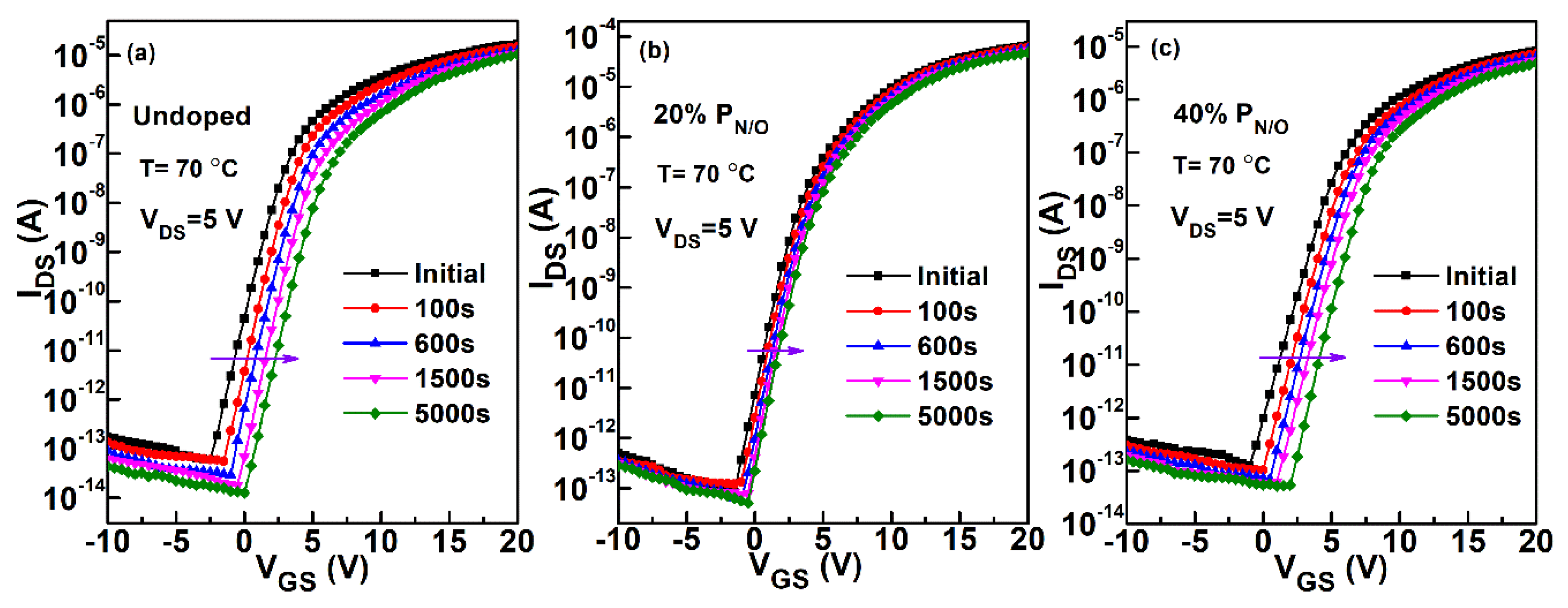
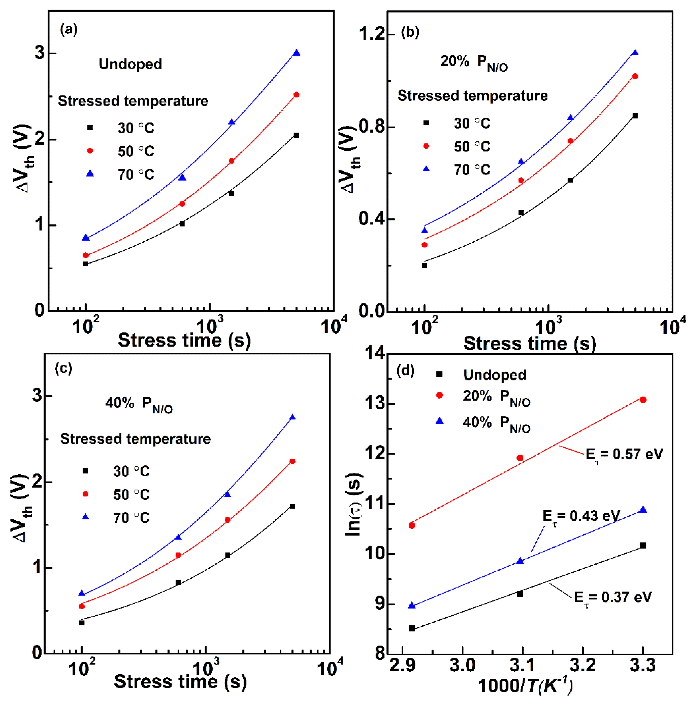
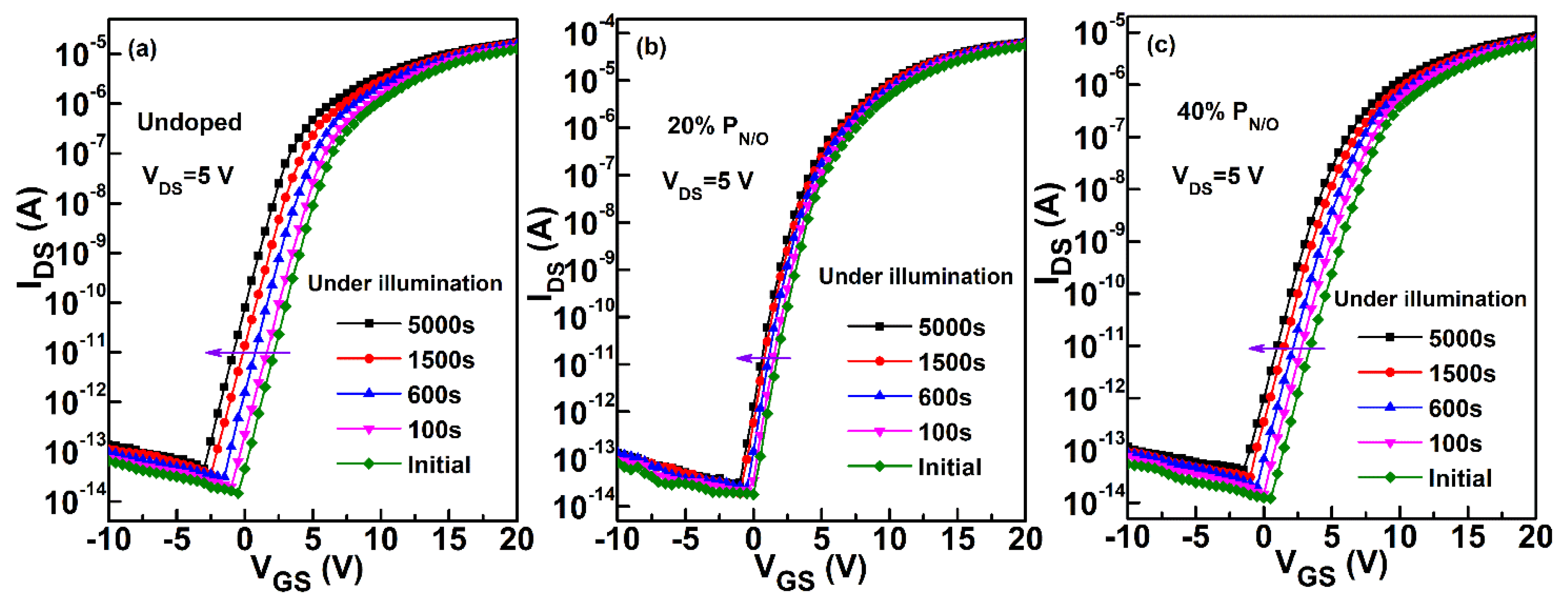
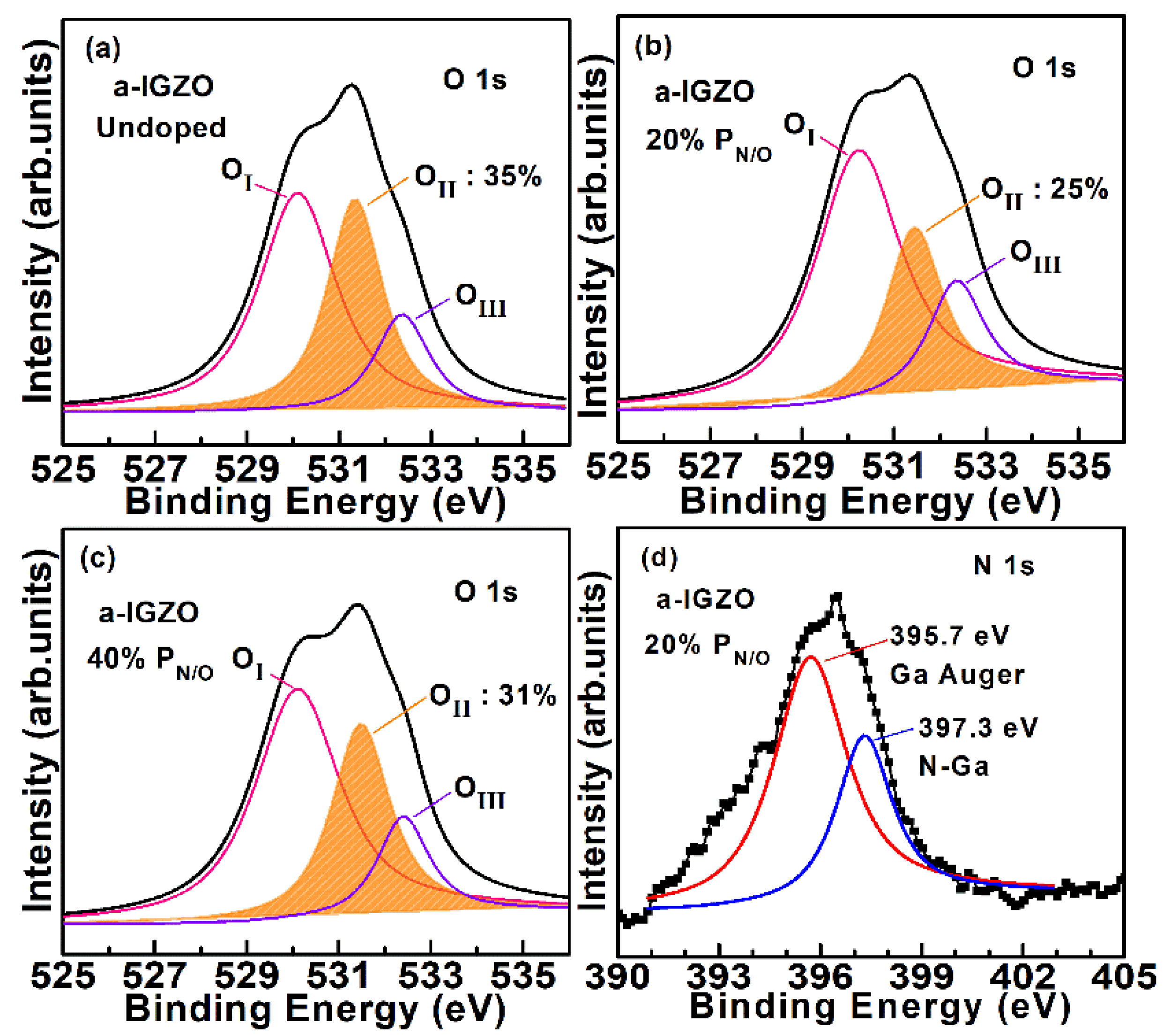
3. Results and Discussion
4. Conclusions
Author Contributions
Funding
Conflicts of Interest
References
- Nomura, K.; Ohta, H.; Takagi, A.; Kamiya, T.; Hirano, M.; Hosono, H. Room-temperature fabrication of transparent flexible thin-film transistors using amorphous oxide semiconductors. Nature 2004, 432, 488. [Google Scholar] [CrossRef] [PubMed]
- Yabuta, H.; Sano, M.; Abe, K.; Aiba, T.; Den, T.; Kumomi, H.; Nomura, K.; Kamiya, T.; Hosono, H. High-mobility thin-film transistor with amorphous InGaZnO4 channel fabricated by room temperature rf-magnetron sputtering. Appl. Phys. Lett. 2006, 89, 112123. [Google Scholar] [CrossRef]
- Nomura, K.; Kamiya, T.; Yanagi, H.; Ikenaga, E.; Yang, K.; Kobayashi, K.; Hirano, M.; Hosono, H. Subgap states in transparent amorphous oxide semiconductor, In-Ga-Zn-O, observed by bulk sensitive X-ray photoelectron spectroscopy. Appl. Phys. Lett. 2008, 92, 202117. [Google Scholar] [CrossRef]
- Kamiya, T.; Nomura, K.; Hosono, H. Origins of High Mobility and Low Operation Voltage of Amorphous Oxide TFTs: Electronic Structure, Electron Transport, Defects and Doping. J. Disp. Technol. 2009, 5, 468–483. [Google Scholar] [CrossRef]
- Suresh, A.; Muth, J.F. Bias stress stability of indium gallium zinc oxide channel based transparent thin film transistors. Appl. Phys. Lett. 2008, 92, 033502. [Google Scholar] [CrossRef]
- Chowdhury, M.D.; Migliorato, H.P.; Jang, J. Time-temperature dependence of positive gate bias stress and recovery in amorphous indium-gallium-zinc-oxide thin-film-transistors. Appl. Phys. Lett. 2011, 98, 153511. [Google Scholar] [CrossRef]
- Huang, X.M.; Wu, C.F.; Lu, H.; Ren, F.F.; Xu, Q.Y.; Ou, H.L.; Zhang, R.; Zheng, Y.D. Electrical instability of amorphous indium-gallium-zinc oxide thin film transistors under monochromatic light illumination. Appl. Phys. Lett. 2012, 100, 243505. [Google Scholar] [CrossRef]
- Kim, C.E.; Yun, I. Effects of nitrogen doping on device characteristics of InSnO thin film transistor. Appl. Phys. Lett. 2012, 100, 013501. [Google Scholar] [CrossRef]
- Abliz, A.; Gao, Q.; Wan, D.; Liu, X.; Xu, L.; Liu, C.; Jiang, C.; Li, X.; Chen, H.; Guo, T.; et al. Effects of Nitrogen and Hydrogen Codoping on the Electrical Performance and Reliability of InGaZnO Thin-Film Transistors. ACS Appl. Mater. Interfaces 2017, 9, 10798–10804. [Google Scholar] [CrossRef] [PubMed]
- Liu, P.T.; Chou, Y.T.; Teng, L.F.; Li, F.H.; Shieh, H.P. Nitrogenated amorphous InGaZnO thin film transistor. Appl. Phys. Lett. 2011, 98, 052102. [Google Scholar] [CrossRef]
- Huang, X.M.; Wu, C.F.; Lu, H.; Ren, F.F.; Chen, D.J.; Zhang, R.; Zheng, Y.D. Enhanced bias stress stability of a-InGaZnO thin film transistors by inserting an ultra-thin interfacial InGaZnO:N layer. Appl. Phys. Lett. 2013, 102, 193505. [Google Scholar] [CrossRef]
- Liu, P.T.; Chang, C.H.; Fuh, C.S.; Liao, Y.T.; Sze, S.M. Effects of Nitrogen on Amorphous Nitrogenated InGaZnO (a-IGZO:N) Thin Film Transistors. J. Disp. Technol. 2016, 12, 1070–1077. [Google Scholar] [CrossRef]
- Raja, J.; Jang, K.; Balaji, N.; Yi, J. Suppression of temperature instability in InGaZnO thin-film transistors by in situ nitrogen doping. Semicond. Sci. Technol. 2013, 28, 115010. [Google Scholar] [CrossRef]
- Raja, J.; Jang, K.; Balaji, N.; choi, W.; Trinh, T.T.; Yi, J. Negative gate-bias temperature stability of N-doped InGaZnO active-layer thin-film transistors. Appl. Phys. Lett. 2013, 102, 083505. [Google Scholar] [CrossRef]
- Lee, J.M.; Cho, I.T.; Lee, J.H.; Kwon, H.I. Bias-stress-induced stretched-exponential time dependence of threshold voltage shift in InGaZnO thin film transistors. Appl. Phys. Lett. 2008, 93, 093504. [Google Scholar] [CrossRef]
- Seo, S.J.; Jeon, J.H.; Hwang, Y.H.; Bae, B.S. Improved negative bias illumination instability of sol-gel gallium zinc tin oxide thin film transistors. Appl. Phys. Lett. 2011, 99, 152102. [Google Scholar] [CrossRef]
- Goto, T.; Imaizumi, F.; Sugawa, S. Improvement in the Negative Bias Illumination Stress Stability for Silicon-Ion Implanted Amorphous InGaZnO Thin-Film Transistors. IEEE Electron Device Lett. 2017, 38, 345. [Google Scholar] [CrossRef]
- Billah, M.M.; Chowdhury, M.D.H.; Mativenga, M.; Um, J.G.; Mruthyunjaya, R.K.; Heiler, G.N.; Tredwell, T.J.; Jang, J. Analysis of Improved Performance Under Negative Bias Illumination Stress of Dual Gate Driving a-IGZO TFT by TCAD Simulation. IEEE Electron Device Lett. 2016, 37, 735. [Google Scholar] [CrossRef]
- Ji, K.H.; Kim, J.I.; Mo, Y.G.; Jeong, J.H.; Yang, S.; Hwang, C.S.; Park, S.H.K.; Ryu, M.K.; Lee, S.Y.; Jeong, J.K. Comparative Study on Light-Induced Bias Stress Instability of IGZO Transistors with SiNx and SiO2 Gate Dielectrics. IEEE Electron Device Lett. 2010, 31, 1404–1406. [Google Scholar] [CrossRef]
- Kim, E.; Jang, W.J.; Kim, W.; Park, J.; Lee, M.K.; Park, S.K.; Choi, K.C. Suppressed Instability of a-IGZO Thin-Film Transistors Under Negative Bias Illumination Stress Using the Distributed Bragg Reflectors. IEEE Trans. Electron Devices 2016, 63, 1066–1071. [Google Scholar] [CrossRef]
- Yang, S.; Ji, K.H.; Kim, U.K.; Hwang, C.S.; Park, S.K.; Hwang, C.S.; Jang, J.; Jeong, J.K. Suppression in the negative bias illumination instability of Zn-Sn-O transistor using oxygen plasma treatment. Appl. Phys. Lett. 2011, 99, 102103. [Google Scholar] [CrossRef]
- Jiang, Y.; Wang, Q.; Zhang, F.; Li, L.; Zhou, D.; Liu, Y.; Wang, D.; Ao, J.P. Reduction of leakage current by O2 plasma treatment for device isolation of AlGaN/GaN heterojunction field effect transistors. Appl. Surf. Sci. 2015, 351, 1155–1160. [Google Scholar] [CrossRef]


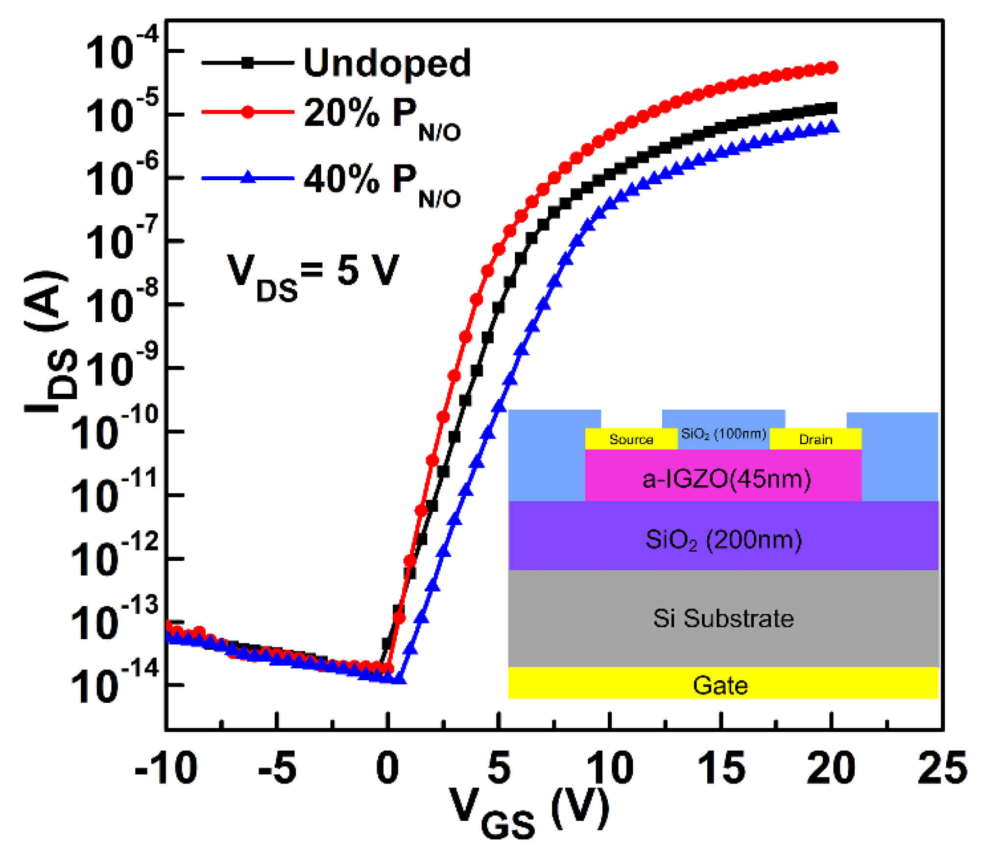
| PN/O (%) | Vth (V) | μFE (cm2/Vs) | SS (V/dec) | Ion/off |
|---|---|---|---|---|
| 0 | 5.0 | 2.2 | 0.8 | >108 |
| 20 | 3.8 | 8.0 | 0.6 | >109 |
| 40 | 7.0 | 1.2 | 0.9 | >107 |
© 2019 by the authors. Licensee MDPI, Basel, Switzerland. This article is an open access article distributed under the terms and conditions of the Creative Commons Attribution (CC BY) license (http://creativecommons.org/licenses/by/4.0/).
Share and Cite
Huang, X.; Zhou, D.; Xu, W. Influence of N2/O2 Partial Pressure Ratio during Channel Layer Deposition on the Temperature and Light Stability of a-InGaZnO TFTs. Appl. Sci. 2019, 9, 1880. https://doi.org/10.3390/app9091880
Huang X, Zhou D, Xu W. Influence of N2/O2 Partial Pressure Ratio during Channel Layer Deposition on the Temperature and Light Stability of a-InGaZnO TFTs. Applied Sciences. 2019; 9(9):1880. https://doi.org/10.3390/app9091880
Chicago/Turabian StyleHuang, Xiaoming, Dong Zhou, and Weizong Xu. 2019. "Influence of N2/O2 Partial Pressure Ratio during Channel Layer Deposition on the Temperature and Light Stability of a-InGaZnO TFTs" Applied Sciences 9, no. 9: 1880. https://doi.org/10.3390/app9091880