Article

High Voltage Graphene Nanowall Trench MOS Barrier Schottky Diode Characterization for High Temperature Applications

by
Rahimah Mohd Saman
*,
Sharaifah Kamariah Wan Sabli
*,
Mohd Rofei Mat Hussin
,
Muhammad Hilmi Othman
,
Muhammad Aniq Shazni Mohammad Haniff
and
Mohd Ismahadi Syono
MIMOS Berhad, Taman Teknologi Malaysia, Bukit Jalil, 57000 Kuala Lumpur, Malaysia
*
Authors to whom correspondence should be addressed.
Appl. Sci. 2019, 9(8), 1587; https://doi.org/10.3390/app9081587
Submission received: 28 December 2018 / Revised: 10 February 2019 / Accepted: 11 February 2019 / Published: 17 April 2019

Abstract

:

Featured Application

This study highlights about graphene nanowall (GNW) application in trench metal-oxide-semiconductor (MOS) barrier Schottky (TMBS) diode for improvement of reversed leakage current at high operating temperature. This novel application will enable designer to develop products with higher energy efficiency.

Abstract

Graphene’s superior electronic and thermal properties have gained extensive attention from research and industrial sectors to study and develop the material for various applications such as in sensors and diodes. In this paper, the characteristics and performance of carbon-based nanostructure applied on a Trench Metal Oxide Semiconductor MOS barrier Schottky (TMBS) diode were investigated for high temperature application. The structure used for this study was silicon substrate with a trench and filled trench with gate oxide and polysilicon gate. A graphene nanowall (GNW) or carbon nanowall (CNW), as a barrier layer, was grown using the plasma enhanced chemical vapor deposition (PECVD) method. The TMBS device was then tested to determine the leakage current at 60 V under various temperature settings and compared against a conventional metal-based TMBS device using TiSi2 as a Schottky barrier layer. Current-voltage (I-V) measurement data were analyzed to obtain the Schottky barrier height, ideality factor, and series resistance (Rs) values. From I-V measurement, leakage current measured at 60 V and at 423 K of the GNW-TMBS and TiSi2-TMBS diodes were 0.0685 mA and above 10 mA, respectively, indicating that the GNW-TMBS diode has high operating temperature advantages. The Schottky barrier height, ideality factor, and series resistance based on dV/dln(J) vs. J for the GNW were calculated to be 0.703 eV, 1.64, and 35 ohm respectively.

1. Introduction

Schottky diodes are widely used in the power electronics industry because of their low forward voltage drop and high switching speed [1]. Low voltage switching power supply and DC-DC converter are among the applications that use Schottky diode technology. However, due to its intrinsic characteristic of increased leakage current at elevated temperature, this limits the operating temperature of the device [2]. It is necessary to ensure that the Schottky diode is operated at the specified temperature to avoid thermal runaway effect, which will cause destructive failure of the device [3]. There are a few methods introduced to overcome thermal runaway. One of the methods employed is by using a trench metal-oxide-semiconductor (MOS) structure to suppress leakage current or electric field [4,5,6,7]. At reverse bias condition, the existence of MOS structures causes charge-coupling along the trench sidewall. The depletion region between the two adjacent MOS transistors will merge resulting in current pinch off, hence altering the electric field distribution at the Schottky interface. This, in turn, shifts the peak of the electrical field away from the Schottky interface to the silicon bulk, allowing reduced leakage current for TMBS diodes. It is still not sufficient, however, to totally eliminate thermal runaway due to limited junction temperature.
To improve this limitation, a new material to replace the conventional metal barrier (titanium silicide (TiSi2), cobalt silicide (CoSi2), and nickel silicide (NiSi2)) is sought. Nanostructured carbon or more specifically graphene material is one of the promising candidates for an alternative metal barrier that could help to improve the limitation of junction temperature as it has metallic behavior with excellent electronic and thermal properties [8,9]. Recently, there have been a number of studies on graphene-silicon Schottky junctions for various applications [10,11,12]. In this work, a graphene nanowall (GNW), also called carbon nanowall (CNW), was used as an alternative metal barrier for a TMBS diode. Graphene nanowalls, with their vertically oriented sheets, have been found to have potential areas of application in field emission, energy storage, gas sensing, biosensors, and lithium-ion batteries [13,14].
Several methods have been employed to grow a GNW layer, but the most popular method is by plasma enhanced chemical vapor deposition (PECVD) because of its feasibility, the potentiality for large-area production, and lower process temperature compared to other methods [15]. In addition to this, a GNW layer can be grown directly on silicon or a silicon oxide surface without a catalyst, thus eliminating possible additional defects and contamination residing on the silicon surface where the layer of interest is in contact with the silicon.
In this work, we demonstrate GNW diode leakage behavior at different temperatures on a trench Schottky diode device. I-V test measurement on the forward bias will be used to extrapolate data to obtain Schottky barrier height, ideality factor, and series resistance. All these data will be compared against a standard commercial TiSi2-based trench Schottky diode (TiSi2-TMBS).

2. Materials and Methods

2.1. Fabrication of Trench MOS Barrier Schottky Structures (TMBS) and Growth of GNW

A trench MOS barrier Schottky diode with blocking voltage capability up to 60 V was fabricated for this study. The substrate used was an n-type lightly doped epitaxial silicon wafer on a highly doped n-type substrate. Active area openings were formed on the epitaxial layer with trench structures (see Figure 1). Polysilicon was used as the gate electrode inside the trenches. An insulating layer, consisting of thermal oxide, insulates the polysilicon and the epitaxial silicon area to form the trench MOS structure. The pre-metal dielectric layer was then deposited and patterned for dry etching of contact opening on the epitaxial layer. The substrate was cleaned with an HF solution to remove native oxide on the contact opening prior to deposition of titanium (Ti) film on the structures to form the Schottky junction. The substrate was then annealed at 700 °C for 60 s to form a titanium silicide (TiSi2) layer on the silicon epi. The TiSi2-TMBS is the baseline sample in this experiment. In the second part of the experiment, TiSi2 was replaced with GNW to form the Schottky contact with silicon epi as discussed below.
The GNW layer was grown in a radio frequency (RF) PECVD chamber from Oxford Instrument. The gases used were acetylene (C2H2) and hydrogen (H2), processed at a low pressure of 800 mTorr and low RF power of 100 W. The substrate heating temperature was 700 °C throughout the growth step of 45 min. For this experiment setting, C2H2 and H2 gases were used in a plasma chamber to grow the GNW on silicon. H2 was used to promote graphitization during the growth process and remove the amorphous carbon. The C2H2 molecules were adsorbed on the silicon surface. Dissociation and out-diffusion of hydrogen occurred leaving carbon atoms on the silicon surface creating nucleation sites [16]. Additional carbon atoms grew the graphene nanosheet on the silicon surface parallel to the substrate until it reached a steady-state growth condition. At this stage, the vertical nanowalls dominated the growth process resulting in the formation of two-dimensional carbon structures with a high aspect ratio.
After the GNW growth completed, a metal layer (Ti) of 200 nm was deposited using RF sputtering method on top of the entire TMBS structure to become the anode. The samples were patterned via photolithography and etched leaving both the GNW and Ti layers on top of the trench areas only. A metal layer was also deposited on the back of the heavily doped substrate which acts as the cathode.

2.2. Characterization

Characterization is divided into two parts; the first part is on the material characterization to understand the quality of the material and the second part is on the electrical characterization for device performance comparison. The surface morphology of the GNW was analyzed using field effect scanning electron microscopy (FESEM) analysis using JEOL JSM-7500F (JEOL Limited, Tokyo, Japan). A cross-sectional image was also taken to find the height of the GNW. Raman spectroscopy measurement was performed using Integra Spectra (NT-MDT Spectrum Instruments, Moscow, Russia) with a 514 nm laser wavelength to investigate the structural properties of the GNW.
The current-voltage (I-V) measurement was done using a Keithley 236 SMU system and micromanipulator prober. As the TMBS diodes used in this experiment are designed for high breakdown voltage (above 60 V), a voltage range between −80 V to 10 V was used to study the device characteristics. I-V curve characteristics are crucial for this study to extract device parameters and analyze the device performance. The measurement was performed with regards to different temperature setting between 298 K and 473 K. Schottky barrier height (фB), ideality factor (n), and series resistance (Rs) were extracted from the forward current and forward current density curves (I-V and J-V). Comparison of I-V curves and device parameters between the GNW-TMBS diode and the conventional TiSi2-TMBS diode were carried out to investigate the effect of vertically standing a few layers of graphene nanostructure on the device characteristics.

3. Results and Discussion

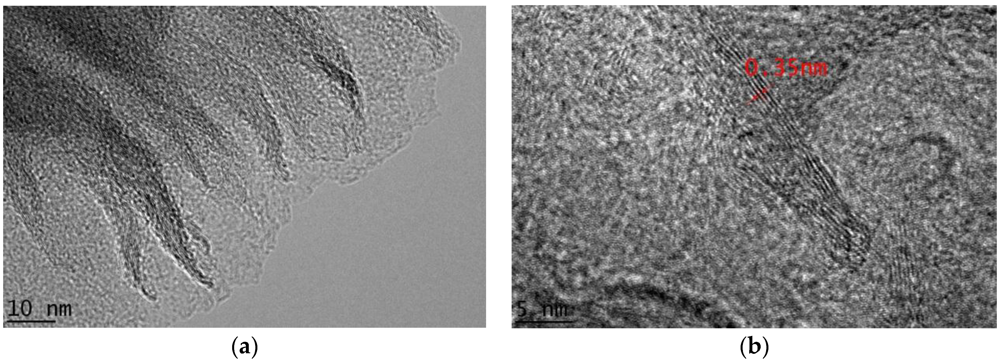
3.1. Material Characterization

FESEM images of the top view and cross-sectional view of the as-grown GNW on the silicon trench structures are shown in Figure 2a,b. The SEM image shows a typical GNW film, with a leaf-like 2D wall structure vertically standing on silicon substrate indicating vertical graphene structure. It was grown directly on silicon surfaces without a metal catalyst. This non-catalytic growth of GNW is defined as self-assembled vertical graphene nanosheets with thicknesses in the range of a few to several nanometers. The height of the GNW in this study is approximately 50 nm to 60 nm, as shown in Figure 2b. The illustration diagram of the GNW structure is shown in Figure 2d, which illustrates the large surface area of freestanding few-layered graphene on silicon substrate. The fin-like protrusions of GNW increased the surface contact with the air, and help to increase the heat dissipation rate, hence eliminate localized self-heating effect in the diode structure. Beside this micro heat sink effect, the high thermal conductivity of the graphene layer also contributes to a high thermal dissipation rate, as reported by several studies on graphene heat spreader in thermal management of electronic devices [17,18,19].
Figure 2c shows the Raman spectrum of the GNW grown on silicon substrates. The result shows typical graphite or nanostructured carbon characteristic of G, D, and 2D peaks. The existence of G and 2D peaks indicates the graphene layer was formed on the silicon substrate. The G peak at 1580 cm−1 indicates the graphitized structures. The D peak at 1360 cm−1 is associated with a defect in the material [12,20] or disorder-induced phonon mode [16], which in this case may relates to a few types of defects, i.e., carbon materials that are not purely a single layer graphene, including amorphous carbon [6] and structural disorder and edges in the GNW layers [13]. The G peak has a shoulder peak on the right side indicating finite-size graphite crystals and graphene edges [21]. The intensity ratio of the G-band to the D-band (IG/ID) is generally related to the in-plane crystallite size of graphene. On the basis of the general Tuinstra−Koenig relation [22], an estimation of the average in-plane crystallite size was obtained using the following empirical formula: La = (2.4 × 10⁻¹⁰)λ4(ID/IG)−1, where λ is the laser excitation wavelength used for the Raman measurements. Here, the La value of the GNW was estimated to be ~7.5 nm for the IG/ID ratio of 0.625 (or ID/IG ratio of 1.6), which is comparable to typical GNWs for thermal management [23]. An I2D/IG ratio of ~1.0 indicates the existence of few layers of graphene sheets with random stacking order in agreement with previous work [24,25]. This observation is also consistent with the high resolution transmission electron microscopy (HRTEM) image of GNWs, as shown in in Figure 3a,b. Several layers of graphene/graphite sheets with an interplanar spacing of 0.35 nm were observed, confirming the GNWs are made of several layers of graphene [12,19,20,21].

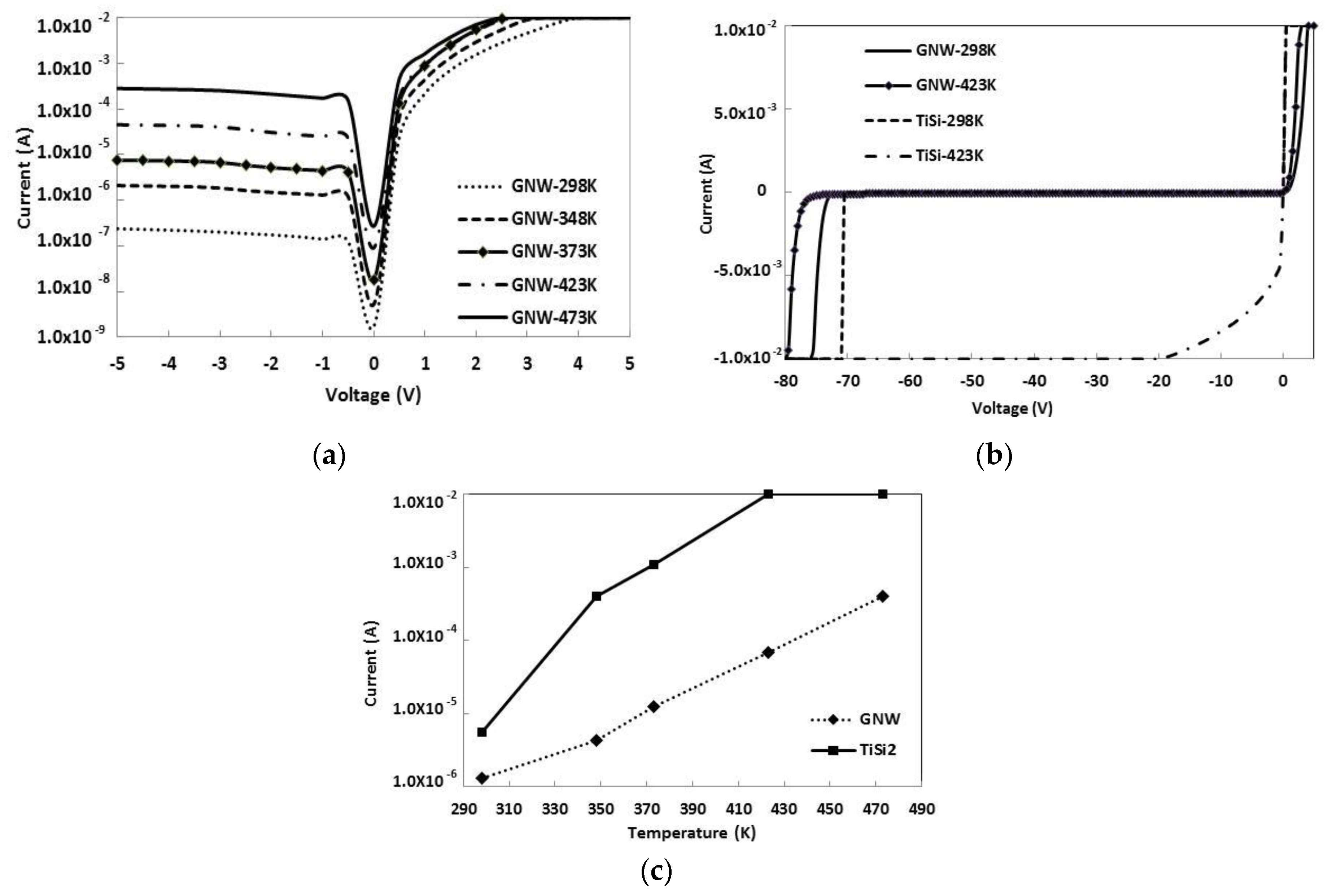
3.2. Electrical Characterization

Recent studies on the graphene-silicon interface showed the Schottky junction is created when graphene or graphene derivatives are in contact with the silicon surface. Figure 4 shows the energy band diagram for graphene-silicon structure. When a graphene layer is in contact with a silicon surface, charge transfer occurs due to a difference in their work functions (фG > фSi) until the respective Fermi levels align at equilibrium condition. The energy diagram shows a discontinuity of the allowed energy states, which results in the formation of an energy barrier at the G/Si interface, known as the Schottky barrier. This energy barrier limits the electron flow from the graphene to the silicon. Schottky barrier height (фB) can be described using the following equation:
фB = фGNWχSi
фB is unaffected by voltage bias and doping level. It can be related to the work function of graphene, фGNW and electron affinity of silicon, χSi. A larger Schottky barrier height normallyshows a better rectifying behavior as reported by Bartomolomeo [11]. This also produces large built-in potential Vbi.
A two-point probe I-V test method was performed on the samples in which the first probe with the voltage applied was placed on the TMBS device and the second probe was grounded on the back of the sample. Both TiSi and GNW TMBS diodes were tested. Figure 5a shows the I-V characteristic of the GNW-TMBS diode exhibiting a rectifying behavior of a Schottky diode at different temperatures. The reverse leakage current at 5 V of the GNW-TMBS diode increased from 0.2 μA to 300 μA when temperature increased from 298 K to 473 K.
Figure 5b shows the leakage current comparison of the GNW-TMBS and TiSi2-TMBS diodes at different temperatures. The I-V curve shows both the GNW-TMBS and TiSi2-TMBS diodes exhibited blocking voltage isabove 60 V at room temperature. The GNW-TMBS diode has a higher breakdown voltage by 5 V. At room temperature, both devices show comparable leakage current. However, at high temperature (>423 K) the TiSi2-TMBS diode shows thermal runaway effect, which the leakage current exponentially increased. On the other hand, the GNW-TMBS diode has low leakage current (<1 mA) when the temperature reaches above 423 K.
Figure 5c shows the temperature effect on leakage current for both GNW and TiSi2-TMBS diodes. The leakage current of the TiSi2-TMBS diode reaches compliance limit (10 mA) once the temperature exceeds 423 K. The GNW-TMBS diode, on the other hand, shows stable leakage current below 1 mA for all the temperature settings. The low leakage current of the GNW-TMBS diode at high temperature could be due to micro heat sink effect resulted from the vertical structure of the GNW layer, as described in Section 3.1 above. As graphene has a high thermal conductivity characteristic, it also helps to reduce or eliminate the localized self-heating effect in the diode structure and effectively dissipate heat from the structure.
In comparison to the TiSi2-silicon interface, the GNW-silicon interface has a more severe inhomogeneity issue, which results in multiple conduction paths through the non-uniform interface. The growth process of GNW on silicon is one of the primary sources of interfacial inhomogeneity, which includes the nucleation sites, patches of graphene nanowall, processing remnants, surface roughness, native oxide, an uneven doping profile, and crystal defects. Since the current tends to take the path of least resistance, patches with low barrier height will preferentially conduct first. The effective barrier height increases when the temperature increases due to the availability of more electrons gaining sufficient energy to overcome the higher barrier height. TiSi2, on the other hand, has better interface homogeneity since it was uniformly grown on silicon as a thin film with fewer defective region. This resulted in TiSi2 having a more stable barrier height with the ideality factor closer to unity. The results are shown in Table 1. The homogeneous interface helps to suppress the multiple conduction paths that contributed to the variation of leakage current.
However, in this study, the GNW showed a higher barrier height as compared to TiSi2, therefore, the leakage current of the GNW-TMBS diode is significantly lower than the TiSi2-TMBS diode. The results are shown in Figure 5c. Theoretically, at escalating temperature, the leakage current increased linearly with the junction temperature as shown in the thermionic emission model. The model highlights the relationship of leakage current and the temperature parameters. We can see the leakage current increased linearly with temperature for both diodes in Figure 5c with the TiSi2-TMBS diode having a higher temperature influence as compared to the GNW-TMBS diode.
We believe that the micro heat sink effect causes the GNW-TMBS diode to experience a lower junction temperature than the actual temperature setting, and this results in a lower temperature effect on the leakage current. Although the homogeneity of TiSi2 is better than GNW, the lack of micro heat sink characteristic in TiSi2 causes a much higher temperature effect on the leakage current. Another study done by Gammon [26] on metal with different homogeneity also showed that inhomogeneous metal would require a large carrier concentration to activate all the patches with low barrier height, while the homogenous interface requiring less carrier concentration to activate the patches. Therefore, the leakage current for the homogeneous interface could be higher than the inhomogeneous surface. The ideality factor for the non-homogenous interface is still higher compared to the homogenous interface, reaching unity at a higher temperature. Based on this explanation, the leakage current for the inhomogeneous interface could be lower than the homogeneous interface because less current can flow through the barrier due to a high activation requirement. Kang [27] in his paper cited that a Schottky diode may exhibit a large leakage current, regardless of having a good ideality factor and the absence of an interface crystal defect.
We have also evaluated GNW-TMBS diodes with various initial leakage current to determine the compatibility of the GNW layer for high temperature applications. From our previous studies on TiSi-TMBS diodes, the diode performance tends to degrade faster with a diode having high initial leakage current and reaches current compliance (10 mA) even at 373 K. As can be seen in Figure S1 and Table S1, the GNW diodes showed a good leakage current performance at different temperatures in which the GNW based diodes can still maintain their leakage current specification limit above 423 K regardless of the initial high leakage current measured at room temperature owing to the GNW’s superior thermal conductivity characteristic.

3.3. Extraction of Schottky Parameters

Important parameters of the Schottky junction, which are Schottky barrier height (фB), ideality factor (n), and series resistance (Rs), are extracted from the forward I-V characteristic at various temperatures. The calculation of the parameters is derived from the Schottky diode equation which follows the thermionic emission model shown in Equation (2) [28,29,30].
I   =   I s [ exp ( q V n k T )   1 ]
where Is is the saturation current, q is the electronic charge, V is the voltage applied on the diode, k is the Boltzmann constant, and T is the absolute temperature. Is can be expressed using Equation (3),
I s =   A A * * T 2 e x p ( q ф B k T ) ,
where A is the area of the diode, A** is the Richardson constant (112 Acm−2·K−2), and фB is the Schottky barrier height. For reliable calculation of the parameters, two methods were used to determine the values of фB, n and Rs, as explained in the subsequent sub-sections.

3.3.1. Method 1: ln (I) vs. V

Equations (2) and (3) when combined with consideration of Vd = V – RsI > 3 kT/q will give the following equation:
I   =   A A * * T 2 e x p ( q ф B k T ) e x p ( q ( V R s I ) n k T ) .
Taking the natural logarithm of Equation (4) will result in
l n   ( I )   =   l n   ( I s ) + q V d n k T   =   l n   ( I s )   +   q ( V R s I ) n k T .
A graph of ln(I) vs. V can then be plotted as shown in Figure 6 and least square fitting is performed in the linear region to determine фB from the y-intercept and n from the slope. For this study, the linear region of the curve is defined from 0 to 0.5 V. Above 0.5 V, the Rs becomes dominant and deviates from the linearity.

3.3.2. Method 2: dV/d(lnJ) vs. J and H(J) vs. J

Since there is a limitation of method 1 to calculate the Rs, method 2 was used in this study to determine the Rs. The Schottky diode parameters were extracted from I-V characteristics, as studied by Cheung [28]. In this method, the resistance Rs is modeled with a series combination of a diode and a resistor. Due to this, the voltage, Vd across the diode can be expressed as the total voltage drop across the diode and resistor. Therefore, the V in Equation (2) is replaced with Vd. With Vd = V − RsI, and Vd > 3kT/q. Equation (2) can then be written as
I   =   I s e x p [ q ( V R s I ) n k T ] .
Rewriting Equation (6) in terms of current density, J, where J is the current divided by the junction area.
V   =   R s A J   +   n ф B +   ( n β ) l n ( J A * * T 2 )
in which β in this Equation (7) equals to q/kT. Taking differentiation from Equation (7) with respect to J and rearranging the terms, Equation (8) is derived as follows:
d V d ( l n ( J ) )   = R s A J   +   n β   .
Another function H(J) was plotted to calculate фB. Value of H(J) is derived from the equation below:
H ( J ) =   V     ( n β )   I n ( J A * * T 2 ) .
From Equation (7), we can deduce H(J) as the following:
H ( J )   =   R s A J   +   n ф B .
The plot of dV/d(lnJ) vs. J in Figure 7a gave a straight line with RsA as the slope and n/β as the y-axis intercept. Plot of H(J) vs. J in Figure 7b derived from Equation (10) also gave a straight line in which the y-axis intercept is equal to B and RsA is the slope. The n value is calculated from Equation (8) to allow the determination of фB from the y-axis intercept value.
Table 1 summarizes the Schottky parameters derived from Methods 1 and 2 for GNW-TMBS and TiSi2-TMBS diodes. The use of standard lnI) vs. V (Method 1) has its limitation in determining the voltage range to use for the calculation of the Schottky barrier height and ideality factor. Even though the condition of V ≥ 3kT/q is satisfied, the I-V curve obtained from the linear region is showing a bowing effect making it difficult to choose a suitable voltage to interpret the Schottky parameters. Several researchers [29,31,32,33] also addressed the same behavior in their papers. It is well-known that the electrical characteristic of a Schottky diode is strongly influenced by ideality factor, series resistance, and leakage current [34,35]. The conventional 1-V curve is suitable for a diode with low series resistance, Rs, in which the Rs can be neglected at low forward bias [35]. However, with high series resistance diode, the inconsideration of Rs will lead to underestimation of фB [36]. Cheung’s method takes into account the influence of series resistance and allows a better estimation of n and фB. However, this method is only applicable at V > 3kT/q [29]. Here, the discussion of the Schottky parameters will be based on Method 2.
From the calculation, фB of the GNW-TMBS diode has higher values by 0.11 eV at 298 K compared to the TiSi2-TMBS diode. The same trend is also observed for other temperature settings. High фB for the GNW-TMBS diode is contributed by a high voltage drop at forward bias as observed in this experiment. The series resistance, Rs, for the GNW is 10 times higher compared to TiSi2 which could be potentially due to high contact resistance between metal to GNW layer, given that all the other processes involved are similar except incorporation of different barrier layer [37,38].
The IV characteristic of the Schottky barrier diode is greatly influenced by metal-semiconductor interface inhomogeneity, which consequently affects the device performance. From Figure 7c and Table 1, we can see that with higher temperature, фB increases for both GNW and TiSi2 TMBS diodes. This characteristic is also reported in several papers with different types of metal and semiconductor materials used in the experiments [32,35,39,40,41,42,43]. The change in фB value can be explained by Tung’s model of barrier inhomogeneity [44]. The barrier inhomogeneity could be due to defects, uneven interface, inhomogeneity in thickness, or presence of insulating patches at the metal-semiconductor interface [35,41,45,46,47,48]. At low temperature, the electrons do not have sufficient energy to surmount the high barrier, however, due to barrier inhomogeneity, current will flow through an area with lower barrier height. With increasing temperature, more and more electrons gain sufficient energy to surmount the higher barrier. As a result, the effective barrier height will increase as the temperature increases.
The ideality factor, n, indicates the conformity of a diode to pure thermionic emission. The n of the GNW diode in this study is higher than unity, but it shows Schottky diode rectifier behavior. It is well-known that graphene on silicon Schottky diodes has a high ideality factor. The values of фB and n reported by other researchers are in the range of 0.41–0.72 and 1.01–7.69 eV, respectively [49,50,51,52,53].
The high n at low temperature is potentially attributed to other transport mechanisms such as generation-recombination of charges in the depletion layer, tunneling of current through the barrier layer, image force lowering and thermionic field emission [31,32,33,50], and lateral distribution of barrier height inhomogeneity besides thermionic charge transport. As temperature increases, the value of n decreases and reaches unity. This behavior indicates that thermionic emission becomes the dominant carrier transport mechanism at a higher temperature [44,50].
The barrier height and ideality factor for GNW showed stable values in the range of 298–323 K, and started to change at 373 K. The change of these values indicates that the thermionic emission mechanism started to dominate the current transport mechanism at high temperature. From the I-V plot in Figure 5a, we can see that the current at the forward region is linear at voltage ≤0.5 V and starts to deviate from linearity due to series resistance, Rs. The double bumps that were normally due to other transport mechanisms such as generation-recombination, thermionic field emission, and field emission, were not observed in this case [26,54,55]. This is also an indication that thermionic emission starts to dominate at the temperature range tested.
At low temperature, two possible mechanisms are responsible for the current flowing through the Schottky junction. The first one is quantum tunneling, which can occur in both forward and reverse bias direction. The mechanism is known as field emission (FE) and if the temperature causes the probability of tunneling to increase, it is known as thermionic field emission (TFE). Quantum tunneling, however, occurs in heavily doped semiconductors with an extremely thin potential barrier, which is not the case for this study. Another mechanism is the generation-recombination of electron-hole pairs in the depletion region that can contribute to the main current component. When applying a voltage to the barrier, the generation rate of the electron-hole pair starts to increase in the depletion region producing current transport between the GNW and the silicon. Generation current is a common cause of the unsaturated current in reverse bias, which clearly can be seen in the I-V curve of the GNW-TMBS diode (Figure 5a).
Looking at Table 1, we can see that the barrier height and ideality factor of the TiSi-TMBS diode did not have significant change until the device was tested at 373 K. We believe since both parameters did not change significantly until 373 K, the major current transport mechanism at that temperature range is thermionic emission. This is supported by the fact that the ideality factor for TiSi2-TMBS is near unity at that temperature range. However, both parameters start to change above 373 K possibly due to the multiplication of a large number of free carriers transported between the metal-semiconductor causing high leakage current.
The GNW film deposited on the silicon interface looks rough and different film height is observed in Figure 8a,b. This is due to the morphology of the GNW layer, as can be seen from Figure 2a,b. The difference in height of the GNW layer and no surface interaction between the GNW and the silicon could cause deviation in the ideality factor and a high barrier height. The TiSi2 surface and interface with silicon in Figure 8c,d is more uniform and smoother. The TiSi2 layer covers the entire silicon interface giving it a near unity in ideality factor. The TiSi2-Si interface is better than the GNW-Si interface because of the interaction of Ti and Si forming the TiSi2 layer.

4. Conclusions

I-V characteristics on TMBS diodes were performed using a graphene nanowall (GNW) as Schottky barrier material. We have shown that this carbon-based material gives an excellent result in leakage current performance at high temperature, surpassing the conventional TMBS diode with TiSi2 as the barrier layer. From the measurement results, GNW has the potential of replacing TiSi2 in lowering leakage, in addition to giving higher breakdown voltage and having the ability to withstand much higher temperature at 473 K without having a thermal runaway on the device tested.
From the forward I-V data at V > 3kT/q, three plots can be generated: ln(I) vs. V, d(V)/d(lnJ) vs. J, and H(J) vs. J. The second and third plots gave linear lines, while the first plot gave a curve requiring linear fitting, which may give error in choosing the data to include in the linear fit. The Schottky barrier parameters, фB, n, and Rs, for GNW at 298 K derived using Cheung’s method, were 0.703 eV, 1.64, and 35 ohm respectively. The major current transport mechanism at a temperature in the range of 298–373 K for the GNW-TMBS diode is thermionic emission. Future work will include contact resistance optimization between GNW to silicon and metal to reduce the resistance effect on фB and study of the GNW Shi density towards Schottky diode device performance.

Supplementary Materials

The following are available online at https://www.mdpi.com/2076-3417/9/8/1587/s1, Figure S1. 5 samples of GNW-TMBS diodes tested at different temperatures, Table S1. Leakage current at different temperatures measured at 60 V for GNW-TMBS and TiSi-TMBS.

Author Contributions

Conceptualization, S.K.W.S. and M.R.M.H.; formal analysis, R.M.S., S.K.W.S., M.R.M.H. and M.H.O.; funding acquisition, M.I.S.; investigation, R.M.S., S.K.W.S., and M.H.O.; methodology, S.K.W.S. and M.R.M.H.; project administration, M.I.S.; Resources, R.M.S., S.K.W.S., and M.H.O.; supervision, M.I.S.; validation, R.M.S., S.K.W.S., M.R.M.H., M.H.O., and M.A.S.M.H.; writing—original draft, R.M.S.; writing—review and editing, R.M.S., S.K.W.S., M.R.M.H., and M.A.S.M.H.

Funding

This research received no external funding.

Acknowledgments

Authors would like to acknowledge Nurul Ainie Ismail, Fauzidah Kassim, and Azhar Idris for assistance in test setup and availability of test tools for device testing.

Conflicts of Interest

The authors declare no conflicts of interest. The funders had no role in the design of the study; in the collection, analyses, or interpretation of data; in the writing of the manuscript, or in the decision to publish the results.

References

  1. Hussin, M.R.M.; Ismail, M.A.; Sabli, S.K.W.; Saidin, N.; Wong, H.Y.; Zaman, M. Design and Fabrication of Low Voltage Silicon Trench MOS Barrier Schottky Rectifier for High Temperature Applications. In Proceedings of the 2015 IEEE 11th International Conference on Power Electronics and Drive Systems, Sydney, NSW, Australia, 9–12 June 2015; pp. 437–441. [Google Scholar]
  2. Rodov, V.; Ankoudinov, A.L.; Taufik, T. Super Barrier Rectifier—A New Generation of Power Diode. In Proceedings of the 22nd Annual IEEE Applied Power Electronics Conference Proceedings, Anaheim, CA, USA, 25 February–1 March 2007; pp. 1053–1056. [Google Scholar]
  3. Baliga, B.J. Fundamentals of Power Semiconductor Devices; Springer Science + Business Multimedia: New York, NY, USA, 2008. [Google Scholar]
  4. Baliga, B.J. Advanced Power Rectifier Concepts; Springer Science + Business Media: New York, NY, USA, 2009; Chapter 5; pp. 117–151. [Google Scholar] [CrossRef]
  5. Mehrotra, M.; Baliga, B.J. Trench MOS Barrier Schottky (TMBS) rectifier: A Schottky rectifier with higher than parallel plane breakdown voltage. Solid-State Electron. 1995, 38, 801–806. [Google Scholar] [CrossRef]
  6. Latorre-Rey, A.D.; Mudholkar, M.; Quddus, M.T. Physics Based Breakdown Voltage Optimization of Tench MOS Barrier Schottky Rectifiers. IEEE Trans. Electron Devices 2018, 65, 1072–1078. [Google Scholar] [CrossRef]
  7. Chen, M.; Kuo, H.; Kim, S. High Voltage TMBS diodes challenge Planar Schottkys. Power Electron. Technol. 2006, 32, 22–32. [Google Scholar]
  8. Khairir, N.S.; Mat Hussin, M.R.; Khairir, M.I.; Uz-Zaman, A.S.M.M.; Abdullah, W.F.H.; Mamat, M.H.; Zoolfakar, A.S. Schottky behavior of reduced graphene oxide at various operating temperatures. Surf. Interfaces 2017, 6, 229–236. [Google Scholar] [CrossRef]
  9. Kaxinta, G.; Hirano, R.; Ayhan, M.E.; Tanemura, M. Fabrication of a Schottky junction diode with direct growth graphene on silicon by a solid phase reaction. J. Phys. D Appl. Phys. 2013, 46, 455103. [Google Scholar]
  10. Li, X.; Zhu, H.; Wang, K.; Cao, A.; Wei, J.; Li, C.; Jia, Y.; Lin, Z.; Li, X.; Wu, D. Graphene-On-Silicon Schottky Junction Solar Cells. Adv. Mater. 2010, 22, 2743–2748. [Google Scholar] [CrossRef]
  11. Di Bartolomeo, A. Graphene Schottky diodes: An experimental review of the rectifying graphene/semiconductor heterojunction. Phys. Rep. 2016, 606, 1–58. [Google Scholar] [CrossRef] [Green Version]
  12. Mohammed, M.; Li, Z.; Cui, J.; Chen, Ta. Junction investigation of graphene/silicon Schottky diodes. Nanoscale Res. Lett. 2012, 7, 302. [Google Scholar] [CrossRef] [PubMed]
  13. Zhao, R.; Ahktar, M.; Aruqi, A.; Dharmasena, R.; Jansinski, J.B.; Thantirige, R.M.; Sumanasakera, G.U. Electrical transport properties of graphene nanowalls grown at low temperature using plasma enhanced vapor deposition. Mater. Res. Express 2017, 4, 055007. [Google Scholar] [CrossRef]
  14. Vizireanu, S.; Nistor, L.; Haupt, M.; Katzenmaier, V.; Oehr, C.; Dinescu, G. Carbon Nanowalls Growth by Radiofrequency Plasma-Beam-Enhanced Chemical Vapor Deposition. Plasma Process. Polym. 2008, 5, 263–268. [Google Scholar] [CrossRef]
  15. Hiramatsu, M.; Shiji, K.; Amano, H.; Hori, M. Fabrication of vertically aligned carbon nanowalls using capacitivelly coupled plasma-enhanced chemical vapor deposition assisted by hydrogen radical injection. Appl. Phys. Lett. 2004, 84, 4708. [Google Scholar] [CrossRef]
  16. Hiramatsu, M.; Kondo, H.; Hori, M. Graphene Nanowalls. New Progress on Graphene Research, Jian Ru Gong, IntechOpen, 2013, doi:10.5772/51528. Available online: https://www.intechopen.com/books/new-progress-on-graphene-research/graphene-nanowalls (accessed on 17 July 2018).
  17. Gao, Z.; Zhang, Y.; Fu, Y.; Yuen, M.M.F.; Liu, J. Thermal chemical vapor deposition grown graphene heat spreader for thermal management of hot spots. Carbon 2013, 61, 342–348. [Google Scholar] [CrossRef]
  18. Subrina, S.; Kotchetkov, D.; Balandin, A.A. Graphene Heat Spreaders for Thermal Management of Nanoelectronic Circuits. IEEE Electron Device Lett. 2009, 30, 1281. [Google Scholar] [CrossRef]
  19. Song, H.; Liu, J.; Liu, B.; Wu, J.; Cheng, Hu.; Kang, F. Two-Dimensional Materials for Thermal Management Applications. Joule 2018, 2, 442–463. [Google Scholar] [CrossRef]
  20. Wall, M. Thermo Scientific, Application Note 52252. The Raman Spectroscopy of Graphene and the Determination of Layer Thickness. Available online: http://tools.thermofisher.com/content/sfs/brochures/AN52252_ E%201111%20LayerThkns_H_1.pdf (accessed on 9 June 2018).
  21. Ferrari, C.; Meyer, J.C.; Scardac, V.; Casiraghi, C.; Lazzeri, M.; Mauri, F.; Piscanec, S.; Jiang, D.; Novoselov, K.S.; Roth, S.; Geim, A.K. Raman Spectrum of graphene and graphene layers. Phys. Rev. Lett. 2006, 97, 187401. [Google Scholar] [CrossRef]
  22. Tuinstra, F.; Koenig, J.L. Raman Spectrum of Graphite. J. Chem. Phys. 1970, 53, 1126. [Google Scholar] [CrossRef]
  23. Zhang, N.; Li, J.; Liu, Z.; Yang, S.; Xu, A.; Chen, D.; Guo, Q.; Wang, G. Direct Synthesis of Vertical Graphene Nanowalls on Glass Substrate for Thermal Management. Mater. Res. Express 2018, 5, 065606. [Google Scholar] [CrossRef]
  24. Liu, J.; Sun, W.; Wei, D.; Song, X.; Jiao, T.; He, S.; Zhang, W.; Du, C. Direct gowth of graphene nanowalls on the crystalline silicon for solar cells. Appl. Phys. Lett. 2015, 106, 043904. [Google Scholar] [CrossRef]
  25. Zhou, Q.; Liu, X.; Zhang, E.; Luo, S.; Shen, W.J.; Yuefeng, W.; Wei, D. The controlled growth of graphene nanowalls on Si for Schottky photodetector. AIP Adv. 2017, 7, 125317. [Google Scholar] [CrossRef] [Green Version]
  26. Gammon, P.M.; Donchev, E.; Pérez-Tomás, A.; Shah, V.A.; Pang, J.S.; Petrov, P.K.; Jennings, M.R.; Fisher, C.A.; Mawby, P.A.; Leadley, D.R.; et al. A study of temperature-related non-linearity at the metal-silicon interface. J. Appl. Phys. 2012, 112, 114513. [Google Scholar] [CrossRef] [Green Version]
  27. Kang, I.-H.; Kim, S.-C.; Moon, J.-H.; Bahng, W.; Kim, N.-K. Fabrication of a 600-V/20-A 4H-SiC schottky barrier diode. J. Korean Phys. Soc. 2014, 64. [Google Scholar] [CrossRef]
  28. Cheung, S.K.; Cheung, N.W. Extraction of Schottky diode parameters from forward current-voltage characteristics. Appl. Phys. Lett. 1986, 49, 85–87. [Google Scholar] [CrossRef]
  29. Kudryk, Y.Y.; Shynkarenko, V.V.; Slipokurov, V.S.; Bigun, R.I.; Kudryk, R.Y. Determination of the Schottky barrier height in diodes based on Au-TiB2-n-SiC 6H from the current-voltage and capacitance-voltage characteristics, Semiconductor Physics. Quantum Electron. Optoelectron. 2014, 17, 398–402. [Google Scholar] [CrossRef]
  30. Nawawi, A.A.; Sultan, S.M.; Rahman, S.F.A.; Pu, S.H.; McBride, J.W.; Wah, L.H. A Study of Different Extraction Techniques of Nanocrystalline Graphite (GNW)/p-type Silicon Schottky Diode Parameters. In Proceedings of the 2017 IEEE Regional Symposium on Micro and Nanoelectronics (RSM), Batu Ferringhi, Malaysia, 23–25 August 2017; pp. 119–122. [Google Scholar]
  31. Aubry, J.; Meyer, F. Schottky diodes with high series resistance: Limitations of forward I-V methods. J. Appl. Phys. 1994, 76, 7973. [Google Scholar] [CrossRef]
  32. Reddy, D.; Reddy, M.; Reddy, N.; Reddy, V. Schottky Barrier Parameters of Pd/Ti Contacts on N-Type InP Revealed from I-V-T And C-V-T Measurements. J. Mod. Phys. 2011, 2, 113–123. [Google Scholar] [CrossRef]
  33. Rhoderick, E.H.; Williams, R. Metal-Semiconductor Contacts; Clarendon Press: Oxford, UK, 1988. [Google Scholar]
  34. Chankaya, G.; Ucar, N. Schottky Barrier Height Dependence on the Metal Work Function for p-type Si Schottky Diodes. Z. Naturforsch 2004, 59a, 795–798. [Google Scholar]
  35. Gholami, S.; Khazbaz, M. Measurement of I-V characteristics of a PtSi/p-Si schottky barrier diode at low temperatures. Int. J. Electr. Comput. Energ. Electron. Commun. Eng. 2011, 5, 1285–1288. [Google Scholar]
  36. Ahmed, K.; Chiang, T. Schottky barrier height extraction from forward current-voltage characteristics of non-ideal diodes with high series resistance. Appl. Phys. Lett. 2013, 102, 042110. [Google Scholar] [CrossRef]
  37. Vanin, M.; Mortensen, J.J.; Kelkkanen, A.K.; Garcia-Lastra, J.M.; Thygesen, K.S.; Jacobsen, K.W. Graphene on metals: A van der Waals density functional study. Phys. Rev. B 2010, 81, 081408(R). [Google Scholar] [CrossRef]
  38. Zong, Z.; Chen, C.-L.; Dokmeci, M.R.; Wan, K. Direct measurement of graphene adhesion on silicon surface by intercalation of nanoparticles. J. Appl. Phys. 2010, 107, 026104. [Google Scholar] [CrossRef] [Green Version]
  39. Shetty, A.; Roul, B.; Mukundan, S.; Mohan, L.; Chandan, G.; Vinoy, K.J.; Krupanidhi, S.B. Temperature dependent electrical characterization of Pt/HfO2/n-GaN metal-insulator semiconductor (MIS) Schottky diodes. AIP Adv. 2015, 5, 097103. [Google Scholar] [CrossRef]
  40. Jyothi, I.; Yang, H.-D.; Shim, K.-H.; Jayardhanam, V.; Kang, S.-M.; Hong, H. Temperature Dependency of Schottky Barrier Parameters of Ti Schottky Contacts to Si-on-Insulator. Mater. Trans. 2013, 54, 1655–1660. [Google Scholar] [CrossRef] [Green Version]
  41. Mahato, S.; Shiwakoti, N.; Kar, A.K. Temperature dependent barrier height and ideality factor of electrodeposited n-CdSe/Cu Schottky barrier diode. AIP Conf. Proc. 2015, 1665, 120011. [Google Scholar] [CrossRef]
  42. Dey, A.; Jana, R.; Dhar, J.; Das, P.; Ray, P.P. Gaussian Distribution of Inhomogeneous Barrier Height of Al/ZnS/ITO Schottky Barrier Diodes. Mater. Today 2018, 5 Pt 3, 9958–9964. [Google Scholar] [CrossRef]
  43. Ravinandan, M.; Rao, P.K.; Reddy, V.R. Temperature dependence of current-voltage (I-V) characteristics of Pt/Au Schottky contacts on n-type GaN. J. Optoelectron. Adv. Mater. 2008, 10, 2787–2792. [Google Scholar]
  44. Tung, R.T. Electron transport at metal-semiconductor interfaces: General theory. Phys. Rev. B 1992, 45, 13509–13523. [Google Scholar] [CrossRef]
  45. Singh, A.; Uddin, M.A.; Sudarshan, T.; Koley, G. Tunable Reverse-Biased Graphene/Silicon Heterojunction Schottky Diode Sensor. Small 2014, 10, 1555–1565. [Google Scholar] [CrossRef]
  46. Li, X.; Lv, Z.; Zhu, H. Carbon/Silicon Heterojunction Solar Cells: State of the Art and Prospects. Adv. Mater. 2015, 27, 6549–6574. [Google Scholar] [CrossRef]
  47. Jabli, F.; Mosbahi, H.; Gassoumi, M.; Gaquierec, C.; Zaidi, M.A.; Maaref, H. Electron/transport in (Mo/Au)/AlGaN/GaN Schottky diode. IOSR J. Appl. Phys. (IOSR-JAP) 2014, 6, 27–34. [Google Scholar] [CrossRef]
  48. Shtepliuk, I.; Iakimov, T.; Khranovskyy, V.; Eriksson, J.; Giannazzo, F.; Yakimova, R. Role of the Potential Barrier in the Electrical Performance of the Graphene/SiC Interface. Crystals 2017, 7, 162. [Google Scholar] [CrossRef]
  49. Chen, Ch.; Aykol, M.; Chang, Ch.; Levi, A.F.J.; Cronin, S.B. Graphene-Silicon Schottky Diodes. Nano Lett. 2011, 11, 1863–1867. [Google Scholar] [CrossRef]
  50. Luongo, G.; Giubileo, F.; Genovese, L.; Iemmo, L.; Martucciello, N.; Di Bartolomeo, A. I-V and C-V Characterization of a High-Responsivity Graphene/Silicon Photodiode with Embedded MOS Capacitor. Nanomaterials 2017, 7, 158. [Google Scholar] [CrossRef]
  51. Shen, J.; Li, X.; Song, X.; Li, X.; Wang, J.; Zhou, Q.; Luo, S.; Feng, W.; Lu, S.; Feng, S.; et al. High-performance Schottky heterojunction photodetector with directly-grown graphene nanowalls as electrodes. Nanoscale 2017, 9, 6020–6025. [Google Scholar] [CrossRef] [PubMed]
  52. Sinha, D.; Lee, J.U. Ideal Graphene/Silicon Schottky Junction Diodes. Nano Lett. 2014, 14, 4660–4664. [Google Scholar] [CrossRef] [PubMed] [Green Version]
  53. Yang, H.; Heo, J.; Park, S.; Song, H.J.; Seo, D.H.; Byun, K.E.; Kim, P.; Yoo, I.; Chung, H.J.; Kim, K. Graphene Barristor, a Triode Device with a Gate-Controlled Schottky Barrier. Science 2012, 336, 1140–1143. [Google Scholar] [CrossRef] [PubMed]
  54. Mtangi, W.; van Rensburg, P.J.J.; Diale, M.; Auret, F.D.; Nyamhere, C.; Nel, J.M.; Chawanda, A. Analysis of current–voltage measurements on Au/Ni/n-GaN Schottky contacts in a wide temperature range. Mater. Sci. Eng. B 2010, 171, 1–4. [Google Scholar] [CrossRef] [Green Version]
  55. Di Bartolomeo, A.; Giubileo, F.; Luongo, G.; Iemmo, L.; Martucciello, N.; Niu, G.; Fraschke, M.; Skibitzki, O.; Schroeder, T.; Lupina, G. Tunable Schottky barrier and high responsivity in graphene/Si-nanotip optoelectronic devices. 2D Mater. 2016, 4. [Google Scholar] [CrossRef]
Figure 1. Cross-sectional diagram of trench Schottky structure with (a) TiSi2 and (b) GNW as Schottky barrier layer.
Applsci 09 01587 g001
Figure 2. FESEM images of the (a) top view of graphene nanowall (GNW) on silicon trench, (b) cross-section of the GNW, (c) Raman spectrum of the GNW showing D, G and 2D peaks, and (d) illustration diagram of GNW on silicon substrate that have an ultra-large surface contact with the air.
Applsci 09 01587 g002
Figure 3. (a) Low-resolution TEM image of GNW and (b) high-resolution TEM image of GNW of several layers of graphene with an interspace layer of 0.35 nm.
Applsci 09 01587 g003
Figure 4. Energy band diagram of graphene on n-type silicon junction.
Applsci 09 01587 g004
Figure 5. (a) Current versus voltage in semilog scale for GNW-TMBS. (b) I-V curves of GNW and TiSi2 diodes showing breakdown voltage. (c) Leakage current versus temperature of GNW and TiSi2-TMBS diodes at 60 V.
Applsci 09 01587 g005
Figure 6. ln (I) vs. V plot using method 1.
Applsci 09 01587 g006
Figure 7. GNW-TMBS diode plots to extract Schottky parameters. (a) dV/dln(J) vs. J and (b) H(J) vs. J. (c) Temperature dependence of ideality factor and barrier height for GNW and TiSi2 based on Cheung’s method.
Applsci 09 01587 g007
Figure 8. Cross-sectional view of TMBS diode at low and high magnification for (a,b) GNW-TMBS diode (c,d) TiSi2-TMBS diode.
Applsci 09 01587 g008
Table 1. Comparison of Schottky parameters of GNW and TiSi2-TMBS diodes.
Temperatureln(I) vs. VdV/dln(J) vs. J and H(J) vs. J
SampleKelvinSBH, фB (eV)nRs (ohm)SBH, фB (eV)nRs (ohm)
GNW2980.7471.485-0.7031.6435.56
3230.7721.376-0.7041.6431.11
3480.8040.836-0.8111.5440.00
3730.890.95-0.7861.4740.00
TiSi22980.5831.133-0.5891.1333.11
3230.5931.081-0.5991.1723.11
3480.6061.006-0.5981.1753.11
3730.6260.898-0.6120.7553.11

