Review

The Growth Methods and Field Emission Studies of Low-Dimensional Boron-Based Nanostructures

State Key Laboratory of Optoelectronic Materials and Technologies, Guangdong Province Key Laboratory of Display Material and Technology, and School of Electronics and Information Technology, Sun Yat-sen University, Guangzhou 510275, China
*
Author to whom correspondence should be addressed.
Appl. Sci. 2019, 9(5), 1019; https://doi.org/10.3390/app9051019
Submission received: 31 January 2019 / Revised: 25 February 2019 / Accepted: 6 March 2019 / Published: 12 March 2019
(This article belongs to the Special Issue Field Emission from Graphene and other Nanostructures)

Abstract

:
Based on the morphology characteristics, low-dimensional (LD) nanostructures with high aspect ratio can be usually divided into nanowire, nanocone, nanotube, nanorod, nanoribbon, nanobelt and so on. Among numerous LD nanostructures, boron-based nanostructures attracted much interest in recent years because they have high melting-point, large electric and thermal conductivity, and low work function. Compared to traditional thermal emission, field emission (FE) has notable advantages, such as lower power dissipation, longer working life, room-temperature operation, higher brightness and faster switching speed. Most studies reveal they have lower turn-on and threshold fields as well as high current density, which are believed as ideal cold cathode nanomaterials. In this review, we will firstly introduce the growth methods of LD boron-based nanostructures (boron monoelement and rare-earth metal hexaboride). Then, we will discuss their FE properties and applications. At last, the conclusions and outlook will be summarized based on the above studies.

1. Introduction

Field emission (FE) is a typical quantum tunneling effect, in which electrons can tunnel through the barrier and enter the vacuum with the help of the applied electric field instead of going across the barrier [1]. R. H. Fowler and L. Nordheim [2] first proposed the classical FE theory (FN theory) for the metallic flat plane in 1928. With the developments of FE theories [3,4,5,6,7,8], different field emitters have been explored, such as microtip or nanotip arrays [9,10,11], thin film [8,12], and low-dimensional (LD) nanostructures [13,14,15]. During the FE studies of metal microtips, it is found that the existence of a field enhancement factor can remarkably decrease the turn-on or threshold field of field emission in comparison with flat plane [16], which can be approximately calculated by the ratio of length to the curvature radius of the tip [1]. Under this circumstance, LD nanostructures (metal and metal oxides [17], carbon-based [13,18,19], silicon-based [20], and III-V group-based [21,22]) nanostructures inevitably attract considerable attention in cold cathode applications because their larger aspect ratio suggests they should have ultrahigh field enhancement factors. There are usually several crucial requirements for ideal nanostructures with excellent FE performances, which are respectively high field enhance factor, low work function, large electrical and thermal conductivity, high melting-point, and strong endurance to harsh conditions [1].
Among numerous LD nanostructure candidates, boron-based nanostructures are believed as ideal cold cathode nanomaterials [23,24,25,26,27,28,29,30,31,32,33,34,35,36,37,38,39,40,41] because they not only can meet the above requirements for FE applications but also have low-density, large Young’s modulus [42] and strong endurance to high current. For example, boron monoelement nanotube (NT) structures [24] have been proven to have metallic conductivity whether their chirality belongs to armchair or zigzag, which are very beneficial for actual FE applications. In addition, rare-earth metal hexaboride (REB6) nanostructures should be very promising nanomaterials for FE application because they possess metallic conductivity, low work function of 2.5~4.4 eV [32,39,40], large current density and stable electron emission ability. Therefore, in this review, we will mainly focus on the recent progress of the growth methods and FE properties of LD boron-based nanostructures (boron monoelement and rare-earth metal hexaborides).

2. The Synthesis of LD Boron-Based Nanostructures
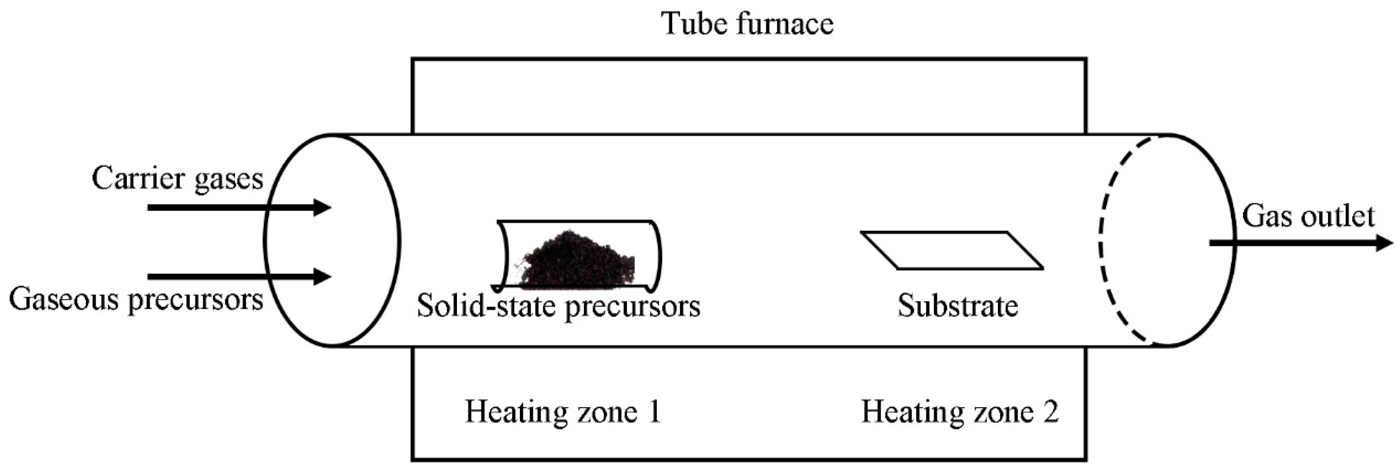
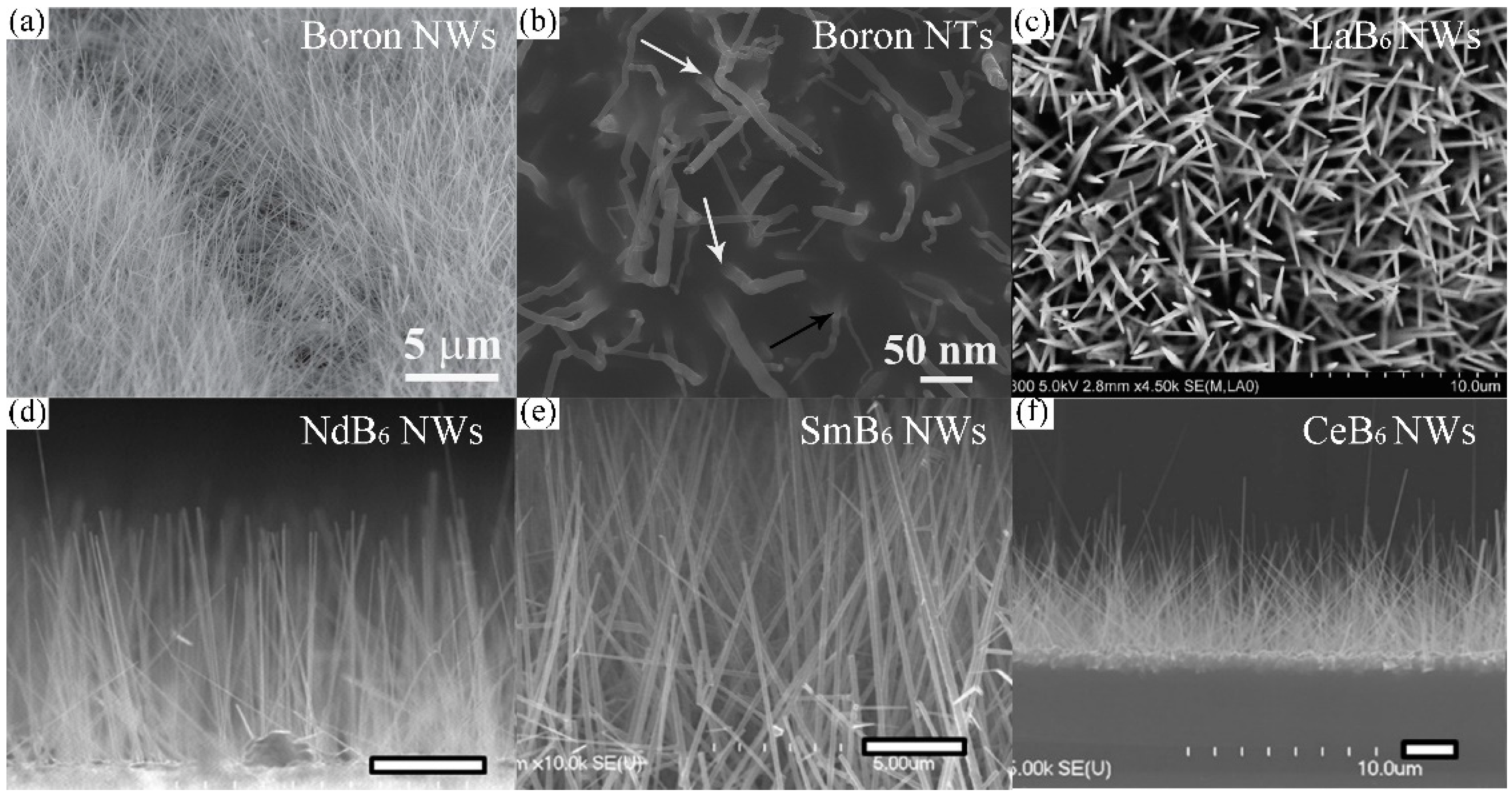
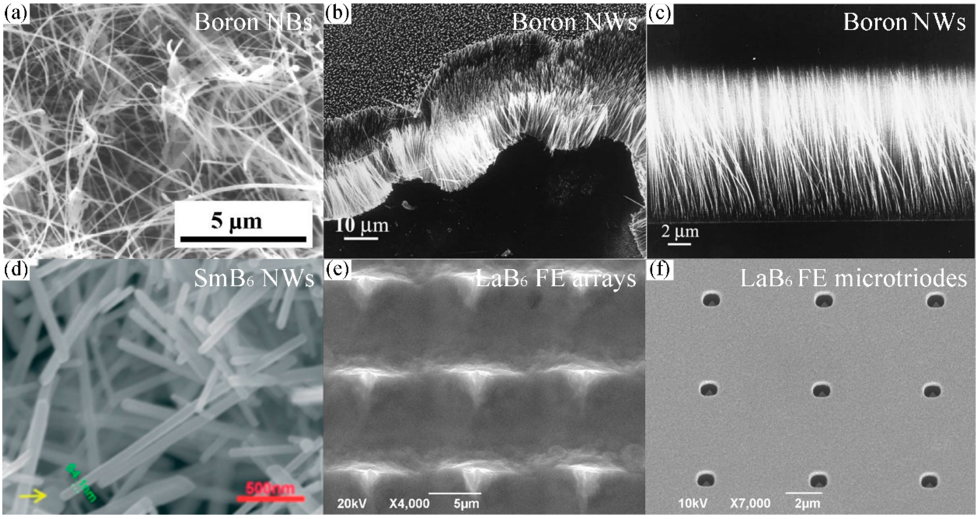
There are some usual fabrication methods for LD boron-based nanostructures, which can be classified into chemical vapor deposition (CVD) [23,24,28,32,43,44,45,46,47,48,49,50,51,52], laser ablation [53,54,55,56,57,58,59], magnetron sputtering [60,61,62,63], solid-state reaction methods [64] etc. In this section, we will review these methods, and discuss the advantages and disadvantages for growing boron-based nanostructures.

2.1. CVD Method

CVD method is a commonly-used way for deposition of thin film. Nowadays, it has been a typical method to grow LD nanostructures, which can be almost suitable for all the reported LD boron-based nanostructures. As shown in Figure 1, vapors, liquids or solids can be chosen as the reaction precursors in CVD method based on the products. In CVD reaction, the transition change from solids or liquids into vapors usually occurs for the precursors at appropriate temperature, and the vapors can be transported to the upsides of substrate and form LD nanostructures via the vapor-liquid-solid (VLS) or vapor-solid (VS) process. In the VLS process, the gas precursors continuously dissolve into the catalyst droplets, and subsequently the solid solutes precipitate from oversaturated droplets and formed the LD nanoamterials with the proceeding of the reaction. Different from the VLS process, the gaseous precursors can directly change into solid-phase nanomaterials without undergoing the intermediate liquid phase in the VS process. In addition, some precursors can be pre-deposited on the substrate and participate in the reaction [39].
Typical morphologies of LD boron-based nanostructures are demonstrated in Figure 2. As seen in Table 1, the boron precursors in these CVD methods can be divided into two categories, which are respectively gaseous and solid phases. As for the use of the gaseous precursors, there are lots of advantages, for example, the morphology control of nanostructures is facilely realized by adjusting the flux or ratio of precursors and the reaction period is relatively shorter. However, the disadvantage for this way is very obvious because these gaseous precursors are usually toxic, flammable or explosive, which inevitably produce potential threat for our daily lives. The other strategy of CVD method is to use B and B2O3 powders as source materials instead of gaseous precursors for preparation of LD boron nanostructures, as described in Refs. [23,24,29,48,65]. Very recently, our group [28,39,66] further developed this method to synthesize the LaB6 and SmB6 nanowires (NWs). In comparison with the CVD method using gaseous precursors, this solid-precursor CVD way often needs relatively higher growth temperature, as seen in Table 1. Therefore, low temperature and environment-friendly growth method remains a challenge for the LD boron-based nanostructures.

2.2. Laser Ablation Way

Laser ablation is also an effective method to fabricate LD boron nanostructures [53,54,55,56,57,58,59]. In laser ablation method, high-power continuous or pulsed laser sources are needed to irradiate the solid precursors and turn them into vapors or plasmas, which are subsequently transferred to the substrate and produce nanostructures. By this way, boron nanobelts (NBs) [55,56,57,58,81] and NWs [53,59] can be fabricated by using a pure boron or a B/NiCo as target, as shown in Figure 3a. Both the boron NBs and NWs were indexed as tetragonal structures. As seen in Table 1, the NBs are observed to have a width-to-thickness ratio of about 5, and their length ranges from several micrometers to millimeters [55]. And the boron NWs have a diameter less than 100 nm and a averaged length of hundreds nanometers [59]. Although laser ablation way has special advantage for growth of high-melting LD boron nanostructures, the experimental equipment is too expensive to be widely used for many researchers compared with CVD methods.

2.3. Magnetron Sputtering Way

Magnetron sputtering way is another synthesis method for boron NWs [60,61,62,63], in which direct-current (DC) or radio frequency (RF) sputtering techniques are used to produce the plasma by bombarding the targets for the formation of nanostructures on substrate [60]. As shown in Figure 3b,c, well-aligned and large-scale boron NW arrays can be prepared on different substrates by this way [60]. The mean length and diameter of the as-grown NWs are tens of micrometers and 45 nm, respectively. However, it is hard to fabricate crystalline boron nanostructures by magnetron sputtering method [62,63].

2.4. Other Methods

Besides the above-mentioned methods, there exist other methods to synthesize LD boron-based nanostructures. By a solid-state reaction way, Y. M. Zhao et al. [64] synthesized single crystalline SmB6 NWs with cubic structure at low temperature of 220~240 °C, and they are 50~120 nm in diameter and 8~12 μm in length. As presented in Figure 3d. X. J. Wang et al. [33,34] respectively prepared the LaB6 FE arrays and microtriodes by etching the LaB6 single crystal or micro-fabrication technology. Single crystalline boron NTs with β-rhombohedral structure can be fabricated in a Cu alloy at 1573 K and separated by 50% HNO3 solution [82]. As described above, there are many choices for preparation of LD boron-based nanostructures, and the researchers should adopt the suitable method by comprehensive consideration of the intrinsic characteristics of the products and the precursors. At the viewpoint of actual FE applications, the CVD method should take great advantages over other methods because the products by CVD way usually have higher crystallinity, larger aspect ratio and better morphology controllability, which corresponds to better FE performances.

3. Field Emission Properties of LD Boron-Based Nanostructures

LD boron-based nanostructures were found to have outstanding FE properties in recent studies. Based on the research goal in experiments, FE measurement techniques can be simply divided into two kinds, which are respectively individual nanostructure and nanostructured film measurement methods. In this section, we will discuss the research advances in FE properties and applications of LD boron-based nanostructures.

3.1. FE Properties of LD Boron-Based Nanostructures

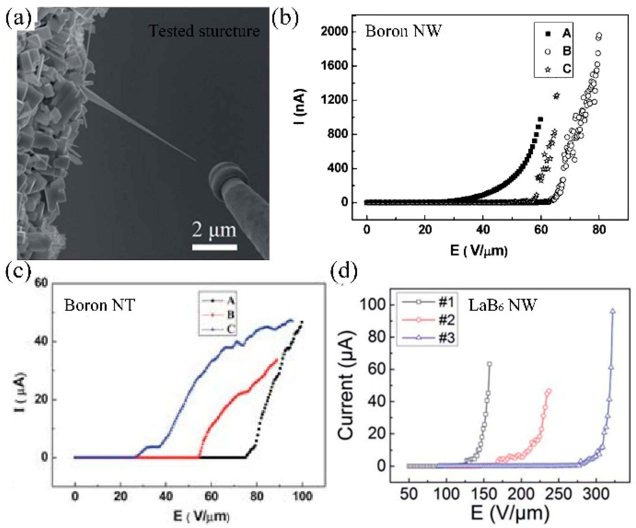
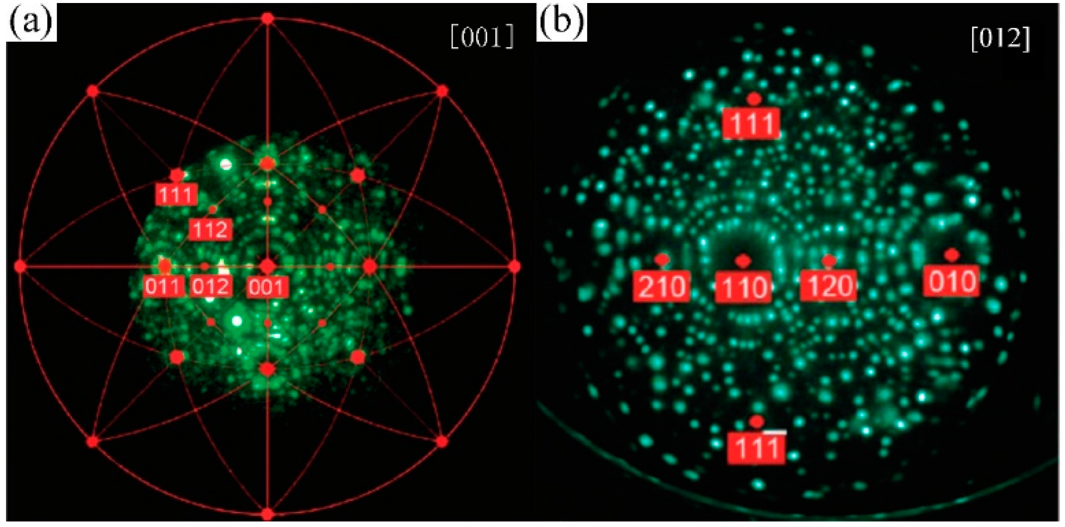
3.1.1. FE Studies of a Single Boron-Based Nanostructure

FE measurement on individual nanostructures are very necessary because of which efficiently avoid the field shielding effect [83,84,85], and thus it can reveal the intrinsic FE properties and mechanisms of LD boron-based nanostructures. There are usually two methods for investigating the FE properties of a single nanostructure. One is W-tip assisted anode probe measurement technique, which can be depicted as follows. In the first step, the researchers are required to peel a suitable single nanowire from the substrate. Subsequently, the researchers need to stick a nanostructure on the W tip by laser welding way. Finally, the emission behaviors of individual nanostructure attaching on the W tip can be studied in the commonly-used FE measurement system, in which a fluorescent screen or metal stage is used as anode probe, and the distance between cathode and anode keeps constant in experiments. The other is in-situ microprobe measurement technique [23,24,25,26,27,28]. By this technique, one can freely manipulate the distance between the W microprobe anode and individual nanostructures on substrate in in-situ microprobe measurement system, in which stepping nanomotor is used to control the movement of microprobe to approach a single nanostructure at nanometer precision in the modified SEM or TEM system. In this system, the electric conductivity and FE behaviors of a single LD boron-based nanostructures as cathode can be easily studied, as indicated in Figure 4a. Compared with W-tip assisted anode probe technique, in-situ microprobe measurement technique has significant merits, such as higher accuracy, more handily manipulation and in-situ observation of the FE behaviors of nanostructures in experiments. As a result, in-situ microprobe measurement technique should a better choice for the studies of individual boron-based or other nanostructures.
Table 2 lists the recent FE results of individual boron-based nanostructures. As seen in Figure 4b,d, the maximum FE currents of a single boron or LaB6 nanostructures are far higher than 1 μA. Especially for individual boron NT and LaB6 NW, their maximum emission current respectively reach as high as 88.9 μA [24] and 96.0 μA [28], which are much better than many other nice cold cathode nanostructures (boron NW [86], GdB6 NW [25] and Mo nanoscrew [87]). Moreover, their FE performances can be comparable to individual carbon NT [88,89] and graphene carbon NT tree with excellent emission performances [90]. However, the FE current stability of boron-based nanostructures needs to be further improved due to their relatively larger current fluctuation.
In addition, J. Tang et al. [40] used field ion microscopy (FIM) and field emission microscopy (FEM) to investigate the emission site distribution of a single LaB6 NW. The FIM patterns of LaB6 NWs with <001> and <012> orientations are respectively demonstrated in Figure 5a,b. It is found that LaB6 NW with <001> orientation has the highest FE symmetry while LaB6 NW with <012> orientation has the lowest apical work function. Also, H. J. Gao et al. [41] researched on the diameter-dependent FE properties of a single boron NW by in-situ microprobe technique. They found that the FE mechanism of individual boron NWs deviates from the classical FN theory when their diameter gradually decreases. Further effort is still needed for mastering the intrinsic FE mechanisms of LD boron-based nanostructures.

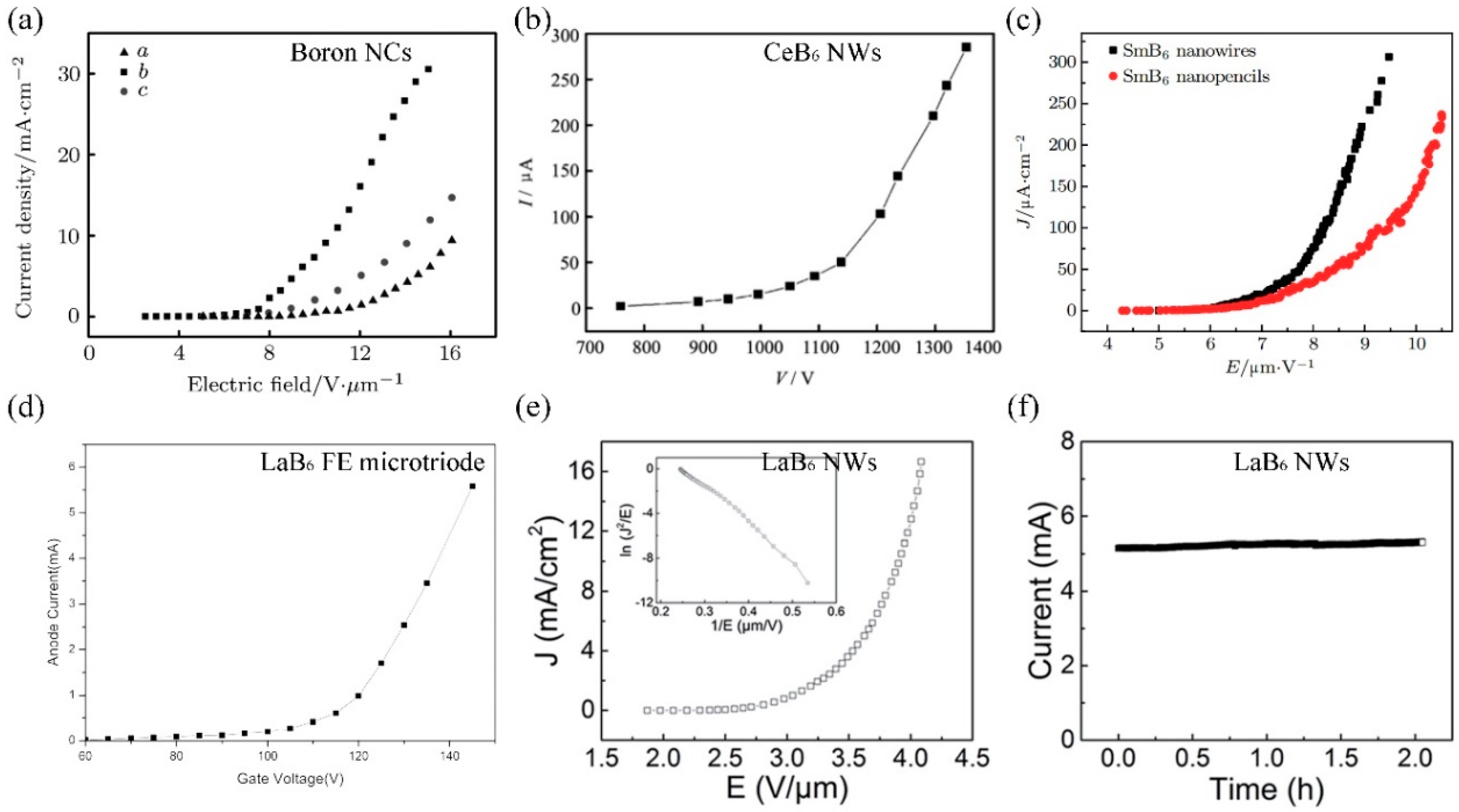
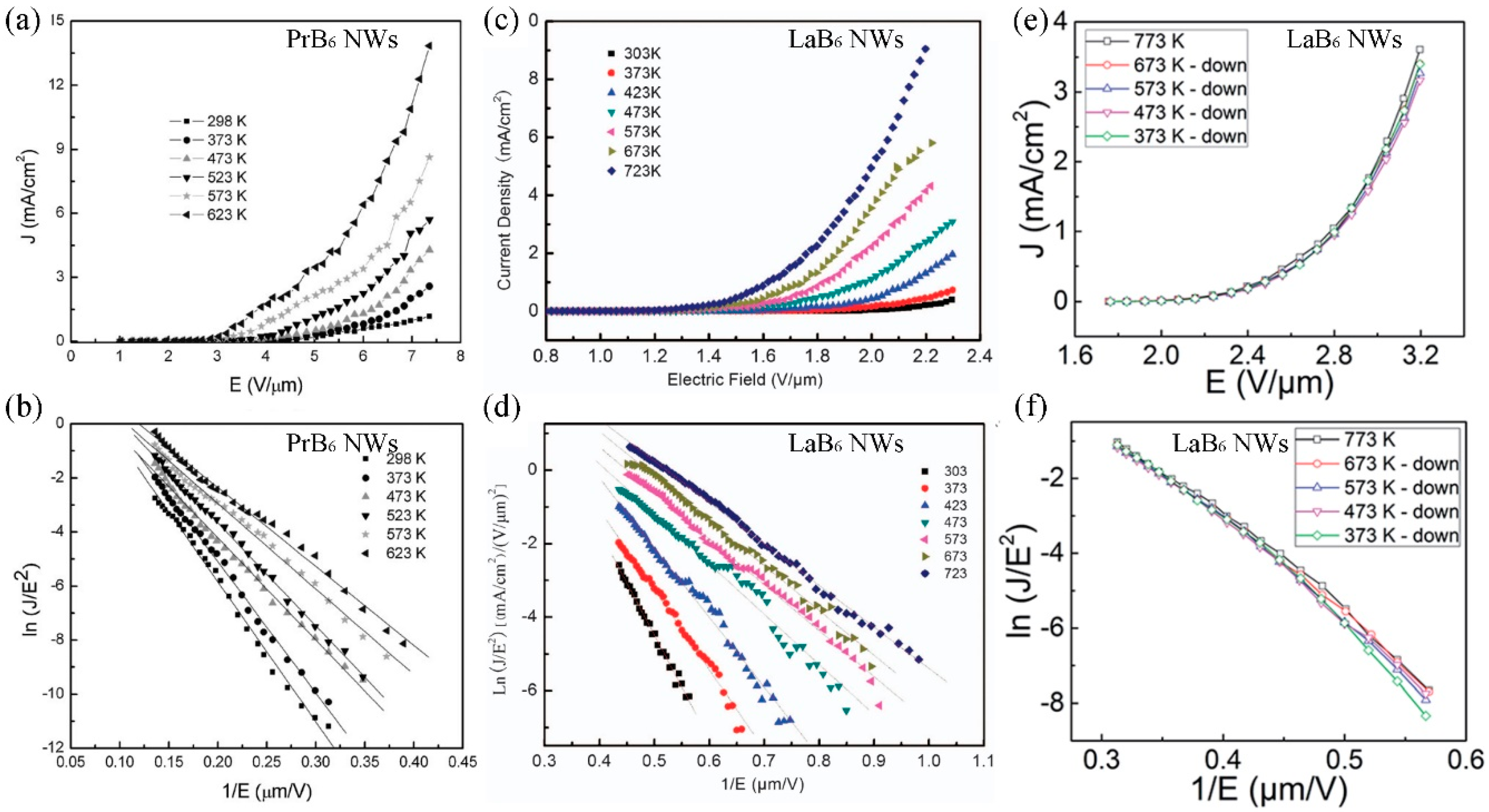
3.1.2. FE Behaviors of Boron-Based Nanostructured Film

The FE properties of boron-based nanostructured film are very significant for evaluating their actual applications, in which the turn-on field and threshold field, current stability and maximum emission current density are the crucial parameters. To investigate the FE properties of boron-based nanostructure film, a column-like probe with smaller diameter of about several mm, a fluorescent screen or a metal platform is often used as an anode. FE current of the nanostructured film sample can be auto-recorded by the programmed amperemeter when the electric voltage is applied between cathode film and anode. Sometimes, a gate voltage may be introduced to assist the anode to extract the electrons from the cathode. Usually, the turn-on and threshold fields are defined as the applied electrical field, corresponding to the FE current density reaches 10 μA/cm2 and 1 mA/cm2. And the current stability directly reflects the current fluctuation at fixed field. There is a very simply and classical calculation expression of current fluctuation Ifluct, i.e., I f l u c t = ( I m a x I m i n ) / ( I m a x + I m i n ) , where Imax and Imin are respectively the maximum and minimum currents at given field during a measurement period over 2 h. It is known to us all that lower turn-on and threshold field as well smaller current fluctuation of nanostructured film suggest that they have excellent FE properties.
The FE properties of LD boron-based nanostructures are listed in Table 3. H. J. Gao’s group [29,30,31] and N. S. Xu’s group [23] separately carried out the FE studies of boron nanostructured film. As shown in Figure 6a, LD boron nanostructures with higher work function and smaller electric conductivity have a relatively higher turn-on field of 2.8~5.1 V/μm and threshold field of 4~10.5 V/μm than LaB6 nanowires (about 2 and 5 V/μm). Meanwhile, the emission current density of boron nanostructured film can reach up to 45 mA/cm2 and their emission current stability is less than 3%. In addition, the patterned boron nanocones (NCs) have better FE properties (such as lower turn-on and threshold fields) compared to the continuous boron NC films [30,31]. Also, the FE properties of REB6 nanostructured films were investigated. As demonstrated in Figure 6b, CeB6 NW film exhibits a turn-on field of 7.6 V/μm and their maximum FE current is about 287 μA. Our group has compared the FE properties of SmB6 NW and nanopencil (NP) films, as seen in Figure 6c. It is found that the SmB6 NWs have a lower turn-on field (6.5 V/μm) than SmB6 NPs (6.9 V/μm), and the maximum emission current density of both nanostructures can reach several hundred µA/cm2. As seen in Figure 6d, X. J. Wang et al. [33,34] found that the emission current density of LaB6 FE microtriode arrays can arrive as high as 558 mA/cm2 at the gate voltage of 145 V. By using a flat metal stage as anode, we [28] investigated the FE properties of LaB6 NWs film with an area of 0.34 cm2. It is seen in Figure 6c,d, the FE current density of LaB6 NW film arrives at 16.7 mA/cm2 and their current fluctuation is only about 1.7% for 2 hour continuous measurements. In addition, J. Q. Xu et al. [23] studied the effect of the morphologies (sparse nanoneedles (NNs), dense NNs, dense nanorods (NRs), and NW arrays) on the FE properties of LaB6 nanostructures, and their turn-on fields were found to be respectively 4.12, 2.16, 2.80 and 1.80 V/μm. In this case, larger aspect ratio is observed to be very essential to lower their turn-on field of LaB6 nanostructures because it represents larger field emission enhancement factors. Also, H. J. Gao et al. [30] investigated the FE properties of different growth density (low, medium, and high) of boron NCs. They found that the boron NCs with medium growth density have the most excellent FE properties (the lowest turn-on and threshold fields). It suggests their FE properties can be improved by adjusting the distance among neighbored boron NCs to close to the length of NCs, which can be attributed to the weakening of field screening effect at suitable nanostructure density. In conclusion, better crystallinity, larger aspect ratio and suitable growth density are highly demanded for the FE applications of LD boron-based nanomaterials.
The temperature-dependent FE properties of LD boron-based nanostructure film also attract researchers’ interest because of which care about their practical applications. Y. M. Zhao et al. [35,37,49] compared the temperature-dependent FE properties among several REB6 NW films. As shown in Figure 7a,b, the research results show that the FE current density of rare-earth hexaboride (LaB6, SmB6, and PrB6) NW film at 573 K increases to be about 10 times larger than that of it at room temperature. J. Q. Xu and our group [28,32] respectively investigated the temperature-dependent FE behaviors of LaB6 nanowire film, as shown in Figure 7c–f. The FE current densities at 723 K and 773 K were observed to respectively increase about 45 and 2.3 times larger than the room-temperature current density. Both of these two research groups attributed the FE improvement mechanism of LaB6 nanowires to the decrease of the effective work function resulting from desorption of the adsorbent gases during temperature-rising process. Moreover, F. Liu et al. [28] found out that the FE current density of LaB6 NWs unvaried with the drop of temperature and almost recovered to the original excellent FE performances after detachment of the surface oxygen molecules in O2 injecting experiments. As seen in Table 3, LD boron-based nanomaterials have comparable FE properties with many excellent cathode nanostructures [87,91,93,94]. Combined the FE performances of individual LD boron-based nanomaterials and nanostructured film, the LD boron-based nanostructures should have promising future in cold cathode electron sources. Of course, the FE current density and stability of LD boron-based nanostructures are worse than thermal emission in present [95,96,97]. Therefore, it is still a long way to fabricate high-quality nanostructures and design a much better FE device structure to enhance their emission performances for actual applications.

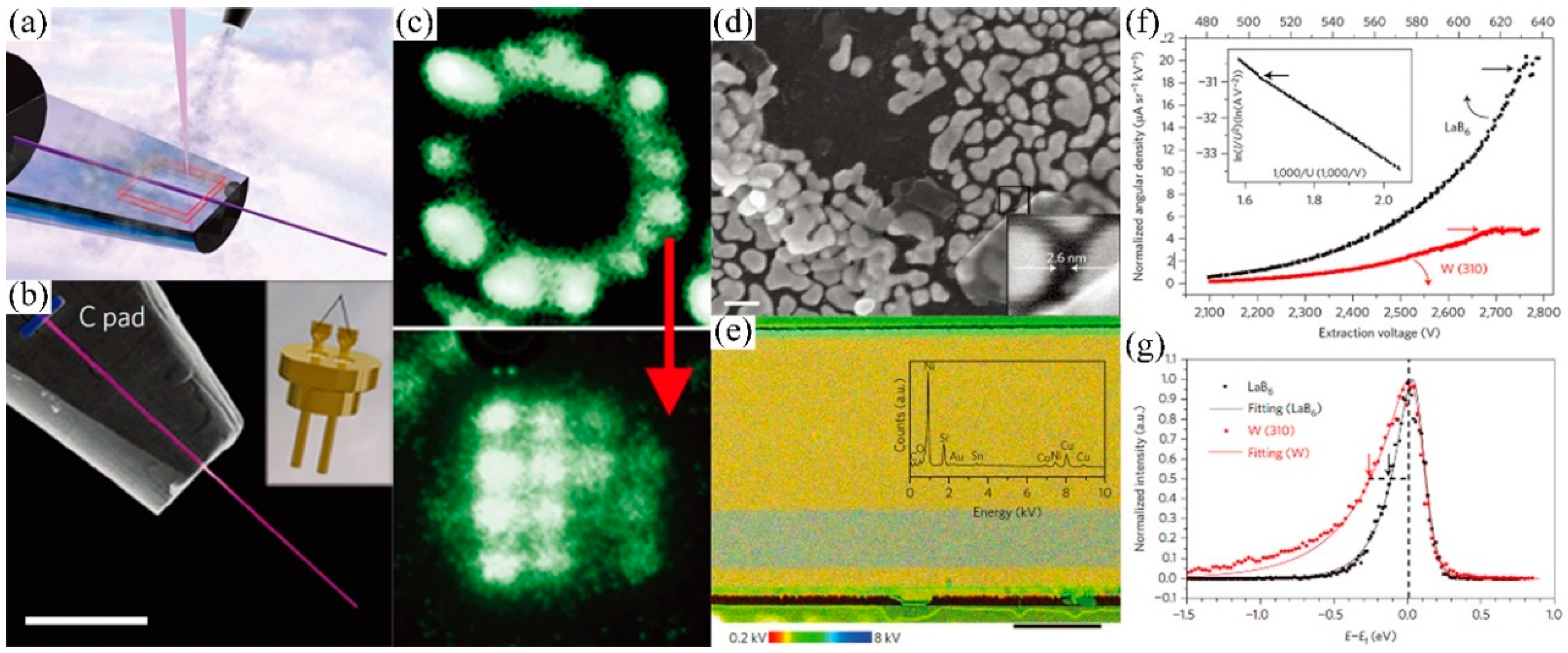
3.2. FE Applications of Boron-Based Nanostructures

In recent studies, low-power nanostructure-based microwave electron tubes were observed to exhibit nice performances, in which 27.5 W output power and 19.5 dB gain have been achieved at a frequency of 10.5 GHz, a helix voltage of 3.35 kV and a cathode current of 58.6 mA [98,99]. In addition, carbon NTs [100,101,102,103,104] and ZnO NWs [105] were used as X-ray sources with a spatial resolution of less than 25 μm. In the meantime, a single LaB6 NW with growing along <001> direction was fabricated into the electron gun of the SEM system by H. Zhang et al. [97] because of its outstanding FE behaviors. As shown in Figure 8, individual LaB6 NW was fixed on the end of W needle as the cathode filament by in-situ e-beam-induced deposition (EBID) technique in the modified SEM system. It was found that the current density gain of LaB6 NW is about 1000 times greater than that of the W(310) tip and no emission decay was observed during tens of hours of operation. Moreover, the SEM equipped with a single LaB6 NW electron source can capture an enough low noise, high resolution (up to 2.6 nm) image and have a rapid mapping ability of chemical compositions at room temperature. N. S. Xu et al. [24] have demonstrated the prototype luminescent tube using boron NT cathode. The luminance of boron NT-based luminescent tube was observed to increase nearly linearly with the cathode current, and the maximum luminance can arrive at 1412 cd/m2 at 3 mA/cm2 current density. Moreover, the boron NT-based luminescent tube exhibited very stable operation and uniform brightness distribution in 2 h continuous measurements, in which the fluctuation was less than 7% and the emission uniformity was over 95 %. Therefore, it suggests that LD boron-based nanostructures should be excellent candidates for future cathode electron source of high-power microwave electron tubes, X-ray tubes or cold cathode electron guns in SEM/TEM system.

4. Outlook and Conclusions

In summary, the researches on the synthesis ways and FE properties of LD boron-based nanostructures have made great progress in the past two decades, but there still exist two big challenges for their future developments. One is the growth of pure boron single crystalline NTs with controlled layers and aspect ratio because the boron NTs with metallic properties usually coexisted with the p-type NWs as well as their length and diameter are hard to control using the known ways. In this situation, the electron transport and FE properties of boron NTs can’t be effectively modulated and improved. The other is to fabricate high-performance LD boron-based nanostructure cathodes to meet the critical requirements for cold cathode electron sources, which can bear enough larger current density with a long lifetime and higher stability. In present studies, the emission current of nearly all individual boron-based nanostructures can arrive at 1 μA current and their maximum current can be even as high as 96.0 μA in measurements [23,24,28,86]. But when their nanostructured film are used, the averaged emission current of a single nanostructure on film is found to be only about 0.2 μA [33], which is far lower than that of individual nanostructure. As a result, the FE performances of LD boron-based nanostructures are not good enough for their cold cathode electron source applications nowadays.
The aim to these two main problems, there are the following possible solutions by our analysis. As for the synthesis of pure boron NTs, the researchers can realize this goal by adjusting the growth parameters, such as heating or cooling rate, the flow rate ratio of carrier gas, the mass ratio of source materials and the collection area of products. If we hope to efficiently improve the FE performances of LD boron-based nanostructure films, two strategies can be considered. One is to control the nanostructure density on substrate, which can effectively decrease the field shielding effect and ensure more nanostructures involve in emission. The other is to enhance the heat dissipation capacity by designing a more effective device structure [106], fabricating composite structure [90], increasing the electron conductivity of boron-based nanostructures by element doping and lowering the contact resistance between nanostructures and substrate, which may remarkably improve their endurance to large emission current.
Considering their excellent emission properties, REB6 nanostructures should have great potential applications as the cold cathode electron sources in SEM/TEM system, high-power microwave electron tubes or X-ray sources. Moreover, boron monoelement nanowires or nanotubes with large Young’s modulus [42] may have a more promising future in portable, flexible and low-power cathode electron sources.

Author Contributions

Formal analysis, H.L. and Z.L.; writing—original draft preparation, H.G., T.Z., Z.G.; writing—review and editing, H.G., J.C., H.C., F.L.; supervision, F.L.; funding acquisition, F.L.

Funding

This work was supported in part by the National Project for the Development of Key Scientific Apparatus of China (2013YQ12034506), National Natural Science Foundation of China (Grant Nos. 51872337, 51290271, 11474364 and 11574129), National Key Basic Research Program of China (Grant No.2013CB933601), the Fundamental Research Funds for the Central Universities of China, the Science and Technology Department of Guangdong Province and the Education Department of Guangdong Province.

Conflicts of Interest

The authors declare no conflict of interest.

References

  1. Xu, N.S.; Huq, S.E. Novel Cold Cathode Materials and Applications. Mater. Sci. Eng. R 2005, 48, 47–189. [Google Scholar] [CrossRef]
  2. Fowler, R.H.; Nordheim, L. Electron Emission in Intense Electric Fields. Proc. R. Soc. Lond. A 1928, 119, 173–181. [Google Scholar] [CrossRef] [Green Version]
  3. Barbour, J.P.; Dolan, W.W.; Trolan, J.K.; Martin, E.E.; Dyke, W.P. Space-Charge Effects in Field Emission. Phys. Rev. 1953, 92, 45–51. [Google Scholar] [CrossRef]
  4. Stratton, R. Theory of Field Emission from Semiconductors. Phys. Rev. 1962, 125, 67–82. [Google Scholar] [CrossRef]
  5. Xu, N.S.; Latham, R.V. Coherently Scattered Hot Electrons Emitted from Mim Graphite Microstructures Deposited on Broad-Area Vacuum-Insulated High-Voltage Electrodes. J. Phys. D Appl. Phys. 1986, 19, 477–482. [Google Scholar] [CrossRef]
  6. Bayliss, K.H.; Latham, R.V. An Analysis of Field-Induced Hot-Electron Emission from Metal-Insulator Microstructures on Broad-Area High-Voltage Electrodes. Proc. R. Soc. A-Math. Phys. Eng. 1986, 403, 285–311. [Google Scholar] [CrossRef]
  7. Geis, M.W.; Efremow, N.N.; Krohn, K.E.; Twichell, J.C.; Lyszczarz, T.M.; Kalish, R.; Greer, J.A.; Tabat, M.D. A New Surface Electron-Emission Mechanism in Diamond Cathodes. Nature 1998, 393, 431–435. [Google Scholar] [CrossRef]
  8. Xu, N.S. Field Emission from Diamond and Related Films. Ultramicroscopy 1999, 79, 59–72. [Google Scholar] [CrossRef]
  9. Spindt, C.A. A Thin-Film Field-Emission Cathode. J. Appl. Phys. 1968, 39, 3504–3505. [Google Scholar] [CrossRef]
  10. Spindt, C.A.; Holland, C.E.; Rosengreen, A.; Brodie, I. Field-Emitter Arrays for Vacuum Microelectronics. IEEE Trans. Electron Devices 1991, 38, 2355–2363. [Google Scholar] [CrossRef]
  11. Thomas, R.N.; Wickstrom, R.A.; Schroder, D.K.; Nathanson, H.C. Fabrication and Some Applications of Large-Area Silicon Field Emission Arrays. Solid-State Electron. 1974, 17, 155–163. [Google Scholar] [CrossRef]
  12. Xu, N.S.; Latham, R.V.; Tzeng, Y. Field-Dependence of the Area-Density of ‘Cold’ Electron Emission Sites on Broad-Area CVD Diamond Films. Electron. Lett. 1993, 29, 1596. [Google Scholar] [CrossRef]
  13. Chen, Y.; Deng, S.Z.; Xu, N.S.; Chen, J.; Ma, X.C.; Wang, E.G. Physical Origin of Non-Linearity in Fowler-Nordheim Plots of Aligned Large Area Multi-Walled Nitrogen-Containing Carbon Nanotubes. Mater. Sci. Eng. A 2002, 327, 16–19. [Google Scholar] [CrossRef]
  14. Li, Y.B.; Bando, Y.; Golberg, D. Quasi-Aligned Single-Crystalline W18O49 Nanotubes and Nanowires. Adv. Mater. 2003, 15, 1924–1926. [Google Scholar] [CrossRef]
  15. Lee, C.J.; Lee, T.J.; Lyu, S.C.; Zhang, Y.; Ruh, H.; Lee, H.J. Field Emission from Well-Aligned Zinc Oxide Nanowires Grown at Low Temperature. Appl. Phys. Lett. 2002, 81, 3648. [Google Scholar] [CrossRef]
  16. Tomaschke, H.; Alpert, D. Field Emission from a Multiplicity of Emitters on a Broad-Area Cathode. J. Appl. Phys. 1967, 38, 881–883. [Google Scholar] [CrossRef]
  17. Zhou, J.; Xu, N.S.; Deng, S.Z.; Chen, J.; She, J.C.; Wang, Z.L. Large-Area Nanowire Arrays of Molybdenum and Molybdenum Oxides: Synthesis and Field Emission Properties. Adv. Mater. 2003, 15, 1835–1840. [Google Scholar] [CrossRef]
  18. Wong, K.W.; Zhou, X.T.; Au, F.C.K.; Lai, H.L.; Lee, C.S.; Lee, S.T. Field-Emission Characteristics of SiC Nanowires Prepared by Chemical-Vapor Deposition. Appl. Phys. Lett. 1999, 75, 2918–2920. [Google Scholar] [CrossRef]
  19. Wu, Z.S.; Pei, S.F.; Ren, W.C.; Tang, D.M.; Gao, L.B.; Liu, B.L.; Li, F.; Liu, C.; Cheng, H.M. Field Emission of Single-Layer Graphene Films Prepared by Electrophoretic Deposition. Adv. Mater. 2009, 21, 1756–1760. [Google Scholar] [CrossRef]
  20. Au, F.C.K.; Wong, K.W.; Tang, Y.H.; Zhang, Y.F.; Bello, I.; Lee, S.T. Electron Field Emission from Silicon Nanowires. Appl. Phys. Lett. 1999, 75, 1700–1702. [Google Scholar] [CrossRef]
  21. He, J.H.; Yang, R.S.; Chueh, Y.L.; Chou, L.J.; Chen, L.J.; Wang, Z.L. Aligned Aln Nanorods with Multi-Tipped Surfaces-Growth, Field-Emission, and Cathodoluminescence Properties. Adv. Mater. 2006, 18, 650–654. [Google Scholar] [CrossRef]
  22. Liu, B.; Bando, Y.; Tang, C.; Xu, F.; Hu, J.; Golberg, D. Needlelike Bicrystalline Gan Nanowires with Excellent Field Emission Properties. J. Phys. Chem. B 2005, 109, 17082–17085. [Google Scholar] [CrossRef]
  23. Liu, F.; Tian, J.F.; Bao, L.H.; Yang, T.Z.; Shen, C.M.; Lai, X.Y.; Xiao, Z.M.; Xie, W.G.; Deng, S.Z.; Chen, J.; et al. Fabrication of Vertically Aligned Single-Crystalline Boron Nanowire Arrays and Investigation of Their Field-Emission Behavior. Adv. Mater. 2008, 20, 2609–2615. [Google Scholar] [CrossRef]
  24. Liu, F.; Shen, C.M.; Su, Z.J.; Ding, X.L.; Deng, S.Z.; Chen, J.; Xu, N.S.; Gao, H.J. Metal-Like Single Crystalline Boron Nanotubes: Synthesis and in Situ Study on Electric Transport and Field Emission Properties. J. Mater. Chem. 2010, 20, 2197. [Google Scholar] [CrossRef]
  25. Zhang, H.; Zhang, Q.; Zhao, G.P.; Tang, J.; Zhou, O.; Qin, L.C. Single-Crystalline Gdb6 Nanowire Field Emitters. J. Am. Chem. Soc. 2005, 127, 13120–13121. [Google Scholar] [CrossRef]
  26. Zhang, H.; Tang, J.; Zhang, Q.; Zhao, G.P.; Yang, G.; Zhang, J.; Zhou, O.; Qin, L.C. Field Emission of Electrons from Single LaB6 Nanowires. Adv. Mater. 2006, 18, 87–91. [Google Scholar] [CrossRef]
  27. Zhang, H.; Tang, J.; Zhang, Q.; Zhou, O.; Qin, L.C. An in Situ Tem Study of Field Emission of Electrons from LaB6 Nanowires. Microsc. Microanal. 2007, 13, 780–781. [Google Scholar] [CrossRef]
  28. Gan, H.B.; Peng, L.X.; Yang, X.; Tian, Y.; Xu, N.S.; Chen, J.; Liu, F.; Deng, S.Z. A Moderate Synthesis Route of 5.6 mA-Current LaB6 Nanowire Film with Recoverable Emission Performance Towards Cold Cathode Electron Source Applications. RSC Adv. 2017, 7, 24848–24855. [Google Scholar] [CrossRef]
  29. Wang, X.J.; Tian, J.F.; Yang, T.Z.; Bao, L.H.; Hui, C.; Liu, F.; Shen, C.M.; Xu, N.S.; Gao, H.J. Single Crystalline Boron Nanocones: Electric Transport and Field Emission Properties. Adv. Mater. 2007, 19, 4480–4485. [Google Scholar] [CrossRef]
  30. Li, C.; Tian, Y.; Wang, D.K.; Shi, X.Z.; Hui, C.; Shen, C.M.; Gao, H.J. Tuning Field Emission Properties of Boron Nanocones with Catalyst Concentration. Chin. Phys. B 2011, 20, 037903. [Google Scholar] [CrossRef]
  31. Li, C.; Tian, Y.; Hui, C.; Tian, J.F.; Bao, L.H.; Shen, C.M.; Gao, H.J. Field Emission Properties of Patterned Boron Nanocones. Nanotechnology 2010, 21, 325705. [Google Scholar] [CrossRef] [PubMed]
  32. Xu, J.Q.; Hou, G.H.; Li, H.Q.; Zhai, T.Y.; Dong, B.P.; Yan, H.L.; Wang, Y.R.; Yu, B.H.; Bando, Y.; Golberg, D. Fabrication of Vertically Aligned Single-Crystalline Lanthanum Hexaboride Nanowire Arrays and Investigation of Their Field Emission. NPG Asia Mater. 2013, 5, e53. [Google Scholar] [CrossRef]
  33. Wang, X.J.; Jiang, Y.D.; Lin, Z.L.; Qi, K.C.; Dong, J.K. Fabrication and Emission Properties of LaB6 Field Emission Microtriode. Proc. SPIE (Chengdu) 2009, 7284, 728411. [Google Scholar]
  34. Wang, X.J.; Jiang, Y.D.; Lin, Z.L.; Qi, K.C.; Wang, B.L. Field Emission Characteristics of Single Crystal LaB6 Field Emitters Fabricated by Electrochemical Etching Method. J. Phys. D Appl. Phys. 2009, 42, 055409. [Google Scholar] [CrossRef]
  35. Xu, J.Q.; Zhao, Y.M.; Ji, X.H.; Zhang, Q.; Lau, S.P. Growth of Single-Crystalline SmB6 Nanowires and Their Temperature-Dependent Electron Field Emission. J. Phys. D Appl. Phys. 2009, 42, 135403. [Google Scholar] [CrossRef]
  36. Zhao, Y.; Ouyang, L.; Zou, C.; Xu, J.; Dong, Y.; Fan, Q. Field Emission from Single-Crystalline CeB6 Nanowires. J. Rare Earths 2010, 28, 424–427. [Google Scholar] [CrossRef]
  37. Zhang, Q.Y.; Xu, J.Q.; Zhao, Y.M.; Ji, X.H.; Lau, S.P. Fabrication of Large-Scale Single-Crystalline PrB6 Nanorods and Their Temperature-Dependent Electron Field Emission. Adv. Funct. Mater. 2009, 19, 742–747. [Google Scholar] [CrossRef]
  38. Fan, Q.H.; Zhang, Q.Y.; Zhao, Y.M.; Ding, Q.W. Field Emission from One-Dimensional Single-Crystalline NdB6 Nanowires. J. Rare Earths 2013, 31, 145–148. [Google Scholar] [CrossRef]
  39. Yang, X.; Gan, H.B.; Tian, Y.; Xu, N.S.; Deng, S.Z.; Chen, J.; Chen, H.J.; Liang, S.D.; Liu, F. An Easy Way to Controllably Synthesize One-Dimensional SmB6 Topological Insulator Nanostructures and Exploration of Their Field Emission Applications. Chin. Phys. B 2017, 26, 118103. [Google Scholar] [CrossRef]
  40. Zhang, H.; Tang, J.; Yuan, J.; Ma, J.; Shinya, N.; Nakajima, K.; Murakami, H.; Ohkubo, T.; Qin, L.C. Nanostructured LaB6 Field Emitter with Lowest Apical Work Function. Nano Lett. 2010, 10, 3539–3544. [Google Scholar] [CrossRef] [PubMed]
  41. Zhang, C.D.; Cai, J.M.; Gao, M.; Lu, H.L.; Zou, Q.; Tian, J.F.; Hu, H.; Shen, C.M.; Guo, H.M.; Gao, H.J. Local Field Emission of Electrons from an Individual Boron Nanowire at Nanometer Electrode Separation. Appl. Surf. Sci. 2012, 258, 2149–2152. [Google Scholar] [CrossRef]
  42. Liu, F.; Tang, D.M.; Gan, H.; Mo, X.; Chen, J.; Deng, S.; Xu, N.; Bando, Y.; Golberg, D. Individual Boron Nanowire Has Ultra-High Specific Young’s Modulus and Fracture Strength as Revealed by in Situ Transmission Electron Microscopy. ACS Nano 2013, 7, 10112–10120. [Google Scholar] [CrossRef] [PubMed]
  43. Ciuparu, D.; Klie, R.F.; Zhu, Y.M.; Pfefferle, L. Synthesis of Pure Boron Single-Wall Nanotubes. J. Phys. Chem. B 2004, 108, 3967–3969. [Google Scholar] [CrossRef]
  44. Xu, T.T.; Zheng, J.G.; Wu, N.Q.; Nicholls, A.W.; Roth, J.R.; Dikin, D.A.; Ruoff, R.S. Crystalline Boron Nanoribbons: Synthesis and Characterization. Nano Lett. 2004, 4, 963–968. [Google Scholar] [CrossRef]
  45. Zhang, H.; Zhang, Q.; Tang, J.; Qin, L.C. Single-Crystalline LaB6 Nanowires. J. Am. Chem. Soc. 2005, 127, 2862–2863. [Google Scholar] [CrossRef] [PubMed]
  46. Xu, J.Q.; Zhao, Y.M.; Zou, C.Y. Self-Catalyst Growth of LaB6 Nanowires and Nanotubes. Chem. Phys. Lett. 2006, 423, 138–142. [Google Scholar] [CrossRef]
  47. Brewer, J.R.; Deo, N.; Morris Wang, Y.; Cheung, C.L. Lanthanum Hexaboride Nanoobelisks. Chem. Mater. 2007, 19, 6379–6381. [Google Scholar] [CrossRef]
  48. Tian, J.; Cai, J.; Hui, C.; Zhang, C.; Bao, L.; Gao, M.; Shen, C.; Gao, H. Boron Nanowires for Flexible Electronics. Appl. Phys. Lett. 2008, 93, 122105. [Google Scholar] [CrossRef]
  49. Xu, J.Q.; Zhao, Y.M.; Zhang, Q.Y. Enhanced Electron Field Emission from Single-Crystalline LaB6 Nanowires with Ambient Temperature. J. Appl. Phys. 2008, 104, 124306. [Google Scholar] [CrossRef]
  50. Jash, P.; Trenary, M. Synthesis of Crystalline Boron Nanoribbons and Calcium Hexaboride Nanowires by Low Pressure Chemical Vapor Deposition. J. Phys. Conf. Ser. 2009, 176, 012011. [Google Scholar] [CrossRef]
  51. Brewer, J.R.; Jacobberger, R.M.; Diercks, D.R.; Cheung, C.L. Rare Earth Hexaboride Nanowires: General Synthetic Design and Analysis Using Atom Probe Tomography. Chem. Mater. 2011, 23, 2606–2610. [Google Scholar] [CrossRef]
  52. Fan, Q.H.; Zhao, Y.M.; Li, D.D. Synthesis of Single-Crystalline Lanthanum Hexaboride Nanowires by Au Catalyst. Ceram. Int. 2013, 39, 6271–6275. [Google Scholar] [CrossRef]
  53. Meng, X.M.; Hu, J.Q.; Jiang, Y.; Lee, C.S.; Lee, S.T. Boron Nanowires Synthesized by Laser Ablation at High Temperature. Chem. Phys. Lett. 2003, 370, 825–828. [Google Scholar] [CrossRef]
  54. Wang, Z.; Sasaki, T.; Shimizu, Y.; Kirihara, K.; Kawaguchi, K.; Kimura, K.; Koshizaki, N. Effect of Substrate Position on the Morphology of Boron Products by Laser Ablation. Appl. Phys. A 2004, 79, 891–893. [Google Scholar] [CrossRef]
  55. Wang, Z.K.; Shimizu, Y.; Sasaki, T.; Kawaguchi, K.; Kimura, K.; Koshizaki, N. Catalyst-Free Fabrication of Single Crystalline Boron Nanobelts by Laser Ablation. Chem. Phys. Lett. 2003, 368, 663–667. [Google Scholar] [CrossRef]
  56. Sato, Y.; Terauchi, M.; Kirihara, K.; Sasaki, T.; Kawaguchi, K.; Koshizaki, N.; Kimura, K. Electron Energy-Loss and Soft X-ray Emission Study of Boron Nanobelts. J. Phys. Conf. Ser. 2009, 176, 012029. [Google Scholar] [CrossRef]
  57. Kirihara, K.; Sasaki, T.; Koshizaki, N.; Kimura, K. Seebeck Coefficient and Power Factor of Single-Crystalline Boron Nanobelts. Appl. Phys. Express 2011, 4, 041201. [Google Scholar] [CrossRef]
  58. Kirihara, K.; Kawaguchi, K.; Shimizu, Y.; Sasaki, T.; Koshizaki, N.; Soga, K.; Kimura, K. Dependence of Photocurrent in Single-Crystalline Boron Nanobelts on Atmosphere. Appl. Phys. Lett. 2006, 89, 243121. [Google Scholar] [CrossRef]
  59. Zhang, Y.; Ago, H.; Yumura, M.; Ohshima, S.; Uchida, K.; Komatsu, T.; Iijima, S. Study of the Growth of Boron Nanowires Synthesized by Laser Ablation. Chem. Phys. Lett. 2004, 385, 177–183. [Google Scholar] [CrossRef]
  60. Cao, L.M.; Zhang, Z.; Sun, L.L.; Gao, C.X.; He, M.; Wang, Y.Q.; Li, Y.C.; Zhang, X.Y.; Li, G.; Zhang, J.; et al. Well-Aligned Boron Nanowire Arrays. Adv. Mater. 2001, 13, 1701–1704. [Google Scholar] [CrossRef]
  61. Cao, L.M.; Hahn, K.; Scheu, C.; Rühle, M.; Wang, Y.Q.; Zhang, Z.; Gao, C.X.; Li, Y.C.; Zhang, X.Y.; He, M.; et al. Template-Catalyst-Free Growth of Highly Ordered Boron Nanowire Arrays. Appl. Phys. Lett. 2002, 80, 4226. [Google Scholar] [CrossRef]
  62. Wang, Y.Q.; Duan, X.F. Crystalline Boron Nanowires. Appl. Phys. Lett. 2003, 82, 272. [Google Scholar] [CrossRef]
  63. Yunpeng, G.; Xu, Z.; Liu, R. Crystalline Boron Nanowires Grown by Magnetron Sputtering. Mater. Sci. Eng. A 2006, 434, 53–57. [Google Scholar] [CrossRef]
  64. Han, W.; Qiu, Y.; Zhao, Y.; Zhang, H.; Chen, J.; Sun, S.; Lan, L.; Fan, Q.; Li, Q. Low-Temperature Synthesis and Electronic Transport of Topological Insulator SmB6 Nanowires. CrystEngComm 2016, 18, 7934–7939. [Google Scholar] [CrossRef]
  65. Yun, S.H.; Wu, J.Z.; Dibos, A.; Gao, X.; Karlsson, U.O. Growth of Inclined Boron Nanowire Bundle Arrays in an Oxide-Assisted Vapor-Liquid-Solid Process. Appl. Phys. Lett. 2005, 87, 113109. [Google Scholar] [CrossRef]
  66. He, X.S.; Gan, H.B.; Du, Z.Z.; Ye, B.C.; Zhou, L.; Tian, Y.; Deng, S.Z.; Guo, G.P.; Lu, H.Z.; Liu, F.; et al. Magnetoresistance Anomaly in Topological Kondo Insulator SmB6 Nanowires with Strong Surface Magnetism. Adv. Sci. 2018, 5, 1700753. [Google Scholar] [CrossRef]
  67. Wu, Y.Y.; Messer, B.; Yang, P.D. Superconducting Mgb2 Nanowires. Adv. Mater. 2001, 13, 1487–1489. [Google Scholar] [CrossRef]
  68. Yang, Q.; Sha, J.; Xu, J.; Ji, Y.J.; Ma, X.Y.; Niu, J.J.; Hua, H.Q.; Yang, D.R. Aligned Single Crystal Boron Nanowires. Chem. Phys. Lett. 2003, 379, 87–90. [Google Scholar] [CrossRef]
  69. Guo, L.; Singh, R.N.; Kleebe, H.J. Nucleation and Growth of Boron Nanowires on Zrb2 Particles. Chem. Vapor Depos. 2006, 12, 448–452. [Google Scholar] [CrossRef]
  70. Yang, Q.; Sha, J.; Wang, L.; Su, Z.; Ma, X.; Wang, J.; Yang, D. Morphology and Diameter Controllable Synthesis of Boron Nanowires. J. Mater. Sci. 2006, 41, 3547–3552. [Google Scholar] [CrossRef]
  71. Xu, J.Q.; Zhao, Y.M.; Shi, Z.D.; Zou, C.Y.; Ding, Q.W. Single-Crystalline SmB6 Nanowires. J. Cryst. Growth 2008, 310, 3443–3447. [Google Scholar] [CrossRef]
  72. Zhou, Y.; Peng, Y.H.; Yin, Y.L.; Zhou, W.C.; Zhou, F.; Liu, C.; Liu, G.T.; Sun, L.F.; Tang, D.S. Large-Scale Synthesis and Electrical Transport Properties of Single-Crystalline SmB6 Nanowires. J. Phys. D Appl. Phys. 2016, 49, 265302. [Google Scholar] [CrossRef]
  73. Zou, C.Y.; Zhao, Y.M.; Xu, J.Q. Synthesis of Single-Crystalline CeB6 Nanowires. J. Cryst. Growth 2006, 291, 112–116. [Google Scholar] [CrossRef]
  74. Zhang, H.; Zhang, Q.; Tang, J.; Qin, L.C. Single-Crystalline CeB6 Nanowires. J. Am. Chem. Soc. 2005, 127, 8002–8003. [Google Scholar] [CrossRef] [PubMed]
  75. Ding, Q.; Zhao, Y.; Xu, J.; Zou, C. Large-Scale Synthesis of Neodymium Hexaboride Nanowires by Self-Catalyst. Solid State Commun. 2007, 141, 53–56. [Google Scholar] [CrossRef]
  76. Xu, J.Q.; Chen, X.L.; Zhao, Y.M.; Zou, C.Y.; Ding, Q.W.; Jian, J.K. Self-Catalyst Growth of Eub6 Nanowires and Nanotubes. J. Cryst. Growth 2007, 303, 466–471. [Google Scholar] [CrossRef]
  77. Xu, J.Q.; Chen, X.L.; Zhao, Y.M.; Zou, C.Y.; Ding, Q.W. Single-Crystalline PrB6 Nanowires and Their Field-Emission Properties. Nanotechnology 2007, 18, 115621. [Google Scholar] [CrossRef]
  78. Chi, M.F.; Zhao, Y.M.; Fan, Q.H.; Han, W. The Synthesis of PrB6 Nanowires and Nanotubes by the Self-Catalyzed Method. Ceram. Int. 2014, 40, 8921–8924. [Google Scholar] [CrossRef]
  79. Gernhart, Z.C.; Jacobberger, R.M.; Wang, L.; Brewer, J.R.; Dar, M.A.; Diercks, D.R.; Mei, W.N.; Cheung, C.L.; Mullins, W. Existence of Erbium Hexaboride Nanowires. J. Am. Ceram. Soc. 2012, 95, 3992–3996. [Google Scholar] [CrossRef]
  80. Liu, F.; Gan, H.B.; Tang, D.M.; Cao, Y.Z.; Mo, X.S.; Chen, J.; Deng, S.Z.; Xu, N.S.; Golberg, D.; Bando, Y. Growth of Large-Scale Boron Nanowire Patterns with Identical Base-up Mode and in Situ Field Emission Studies of Individual Boron Nanowire. Small 2014, 10, 685–693. [Google Scholar] [CrossRef]
  81. Ni, H.; Li, X.D. Synthesis, Structural and Mechanical Characterization of Amorphous and Crystalline Boron Nanobelts. J. Nano Res. 2008, 1, 10–22. [Google Scholar] [CrossRef] [Green Version]
  82. Wu, Y.Y.; Li, Y.F.; Chen, H.W.; Sun, Z.X.; Wang, N.; Qin, J.Y.; Li, H.; Bian, X.F.; Liu, X.F. Growth of Single Crystalline Boron Nanotubes in a Cu Alloy. CrystEngComm 2017, 19, 4510–4518. [Google Scholar] [CrossRef]
  83. Nilsson, L.; Groening, O.; Emmenegger, C.; Kuettel, O.; Schaller, E.; Schlapbach, L.; Kind, H.; Bonard, J.M.; Kern, K. Scanning Field Emission from Patterned Carbon Nanotube Films. Appl. Phys. Lett. 2000, 76, 2071–2073. [Google Scholar] [CrossRef]
  84. Bonard, J.M.; Weiss, N.; Kind, H.; Stöckli, T.; Forró, L.; Kern, K.; Châtelain, A. Tuning the Field Emission Properties of Patterned Carbon Nanotube Films. Adv. Mater. 2001, 13, 184–188. [Google Scholar] [CrossRef]
  85. Teo, K.B.K.; Chhowalla, M.; Amaratunga, G.A.J.; Milne, W.I.; Pirio, G.; Legagneux, P.; Wyczisk, F.; Pribat, D.; Hasko, D.G. Field Emission from Dense, Sparse, and Patterned Arrays of Carbon Nanofibers. Appl. Phys. Lett. 2002, 80, 2011–2013. [Google Scholar] [CrossRef]
  86. Liu, F.; Su, Z.J.; Li, L.; Mo, F.Y.; Jin, S.Y.; Deng, S.Z.; Chen, J.; Shen, C.M.; Gao, H.J.; Xu, N.S. Effect of Contact Mode on the Electrical Transport and Field-Emission Performance of Individual Boron Nanowires. Adv. Funct. Mater. 2010, 20, 1994–2003. [Google Scholar] [CrossRef]
  87. Shen, Y.; Xu, N.S.; Deng, S.Z.; Zhang, Y.; Liu, F.; Chen, J. A Mo Nanoscrew Formed by Crystalline Mo Grains with High Conductivity and Excellent Field Emission Properties. Nanoscale 2014, 6, 4659–4668. [Google Scholar] [CrossRef] [PubMed]
  88. Minoux, E.; Groening, O.; Teo, K.B.; Dalal, S.H.; Gangloff, L.; Schnell, J.P.; Hudanski, L.; Bu, I.Y.; Vincent, P.; Legagneux, P.; et al. Achieving High-Current Carbon Nanotube Emitters. Nano Lett. 2005, 5, 2135–2138. [Google Scholar] [CrossRef]
  89. Xu, Z.; Bai, X.D.; Wang, E.G.; Wang, Z.L. Field Emission of Individual Carbon Nanotube with in Situ Tip Image and Real Work Function. Appl. Phys. Lett. 2005, 87, 163106. [Google Scholar] [CrossRef]
  90. Guo, C.; Xu, N.S.; Zhang, Y.; Ke, Y.L.; Chen, J.; She, J.C.; Deng, S.Z. One-Step Growth of Graphene-Carbon Nanotube Trees on 4″ Substrate and Characteristics of Single Individual Tree. Carbon 2017, 125, 189–198. [Google Scholar] [CrossRef]
  91. Sun, Y.N.; Shin, D.H.; Yun, K.N.; Hwang, Y.M.; Song, Y.N.; Leti, G.; Jeon, S.G.; Kim, J.I.; Saito, Y.; Lee, C.J. Field Emission Behavior of Carbon Nanotube Field Emitters after High Temperature Thermal Annealing. AIP Adv. 2014, 4, 077110. [Google Scholar] [CrossRef]
  92. Zhou, J.; Gong, L.; Deng, S.Z.; Chen, J.; She, J.C.; Xu, N.S.; Yang, R.S.; Wang, Z.L. Growth and Field-Emission Property of Tungsten Oxide Nanotip Arrays. Appl. Phys. Lett. 2005, 87, 223108. [Google Scholar] [CrossRef]
  93. Malesevic, A.; Kemps, R.; Vanhulsel, A.; Chowdhury, M.P.; Volodin, A.; Van Haesendonck, C. Field Emission from Vertically Aligned Few-Layer Graphene. J. Appl. Phys. 2008, 104, 084301. [Google Scholar] [CrossRef]
  94. She, J.C.; Deng, S.Z.; Xu, N.S.; Yao, R.H.; Chen, J. Fabrication of Vertically Aligned Si Nanowires and Their Application in a Gated Field Emission Device. Appl. Phys. Lett. 2006, 88, 013112. [Google Scholar] [CrossRef]
  95. Lafferty, J.M. Boride Cathodes. J. Appl. Phys. 1951, 22, 299–309. [Google Scholar] [CrossRef]
  96. Futamoto, M.; Nakazawa, M.; Usami, K.; Hosoki, S.; Kawabe, U. Thermionic Emission Properties of a Single-Crystal LaB6 Cathode. J. Appl. Phys. 1980, 51, 3869–3876. [Google Scholar] [CrossRef]
  97. Zhang, H.; Tang, J.; Yuan, J.; Yamauchi, Y.; Suzuki, T.T.; Shinya, N.; Nakajima, K.; Qin, L.C. An Ultrabright and Monochromatic Electron Point Source Made of a LaB6 Nanowire. Nat. Nanotechnol. 2016, 11, 273–279. [Google Scholar] [CrossRef]
  98. Qiu, J.X.; Levush, B.; Pasour, J.; Katz, A.; Armstrong, C.M.; Whaley, D.R.; Tucek, J.; Kreischer, K.; Gallagher, D. Vacuum Tube Amplifiers. IEEE Microw. Mag. 2009, 10, 38–51. [Google Scholar] [CrossRef]
  99. Makishima, H.; Imura, H.; Takahashi, M.; Fukui, H.; Okamoto, A. Remarkable Improvements of Microwave Electron Tubes through the Development of the Cathode Materials. In Proceedings of the IEEE 10th International Conference on Vacuum Microelectronics, Kyongju, Korea, 17–21 August 1997; pp. 194–199. [Google Scholar]
  100. Sugie, H.; Tanemura, M.; Filip, V.; Iwata, K.; Takahashi, K.; Okuyama, F. Carbon Nanotubes as Electron Source in an X-ray Tube. Appl. Phys. Lett. 2001, 78, 2578–2580. [Google Scholar] [CrossRef]
  101. Zhang, J.; Yang, G.; Cheng, Y.; Gao, B.; Qiu, Q.; Lee, Y.Z.; Lu, J.P.; Zhou, O. Stationary Scanning X-Ray Source Based on Carbon Nanotube Field Emitters. Appl. Phys. Lett. 2005, 86, 184104. [Google Scholar] [CrossRef]
  102. Qian, X.; Tucker, A.; Gidcumb, E.; Shan, J.; Yang, G.; Calderon-Colon, X.; Sultana, S.; Lu, J.; Zhou, O.; Spronk, D.; et al. High Resolution Stationary Digital Breast Tomosynthesis Using Distributed Carbon Nanotube X-ray Source Array. Med. Phys. 2012, 39, 2090–2099. [Google Scholar] [CrossRef]
  103. Park, S.; Gupta, A.P.; Yeo, S.J.; Jung, J.; Paik, S.H.; Mativenga, M.; Kim, S.H.; Shin, J.H.; Ahn, J.S.; Ryu, J. Carbon Nanotube Field Emitters Synthesized on Metal Alloy Substrate by Pecvd for Customized Compact Field Emission Devices to Be Used in X-ray Source Applications. Nanomaterials 2018, 8, 378. [Google Scholar] [CrossRef] [PubMed]
  104. Gupta, A.P.; Park, S.; Yeo, S.J.; Jung, J.; Cho, C.; Paik, S.H.; Park, H.; Cho, Y.C.; Kim, S.H.; Shin, J.H.; et al. Direct Synthesis of Carbon Nanotube Field Emitters on Metal Substrate for Open-Type X-ray Source in Medical Imaging. Materials 2017, 10, 878. [Google Scholar] [CrossRef] [PubMed]
  105. Chen, D.K.; Song, X.M.; Zhang, Z.P.; Li, Z.P.; She, J.C.; Deng, S.Z.; Xu, N.S.; Chen, J. Transmission Type Flat-Panel X-ray Source Using Zno Nanowire Field Emitters. Appl. Phys. Lett. 2015, 107, 243105. [Google Scholar] [CrossRef]
  106. Utsumi, T. Vacuum Microelectronics: What’s New and Exciting. IEEE Trans. Electron Devices 1991, 38, 2276–2283. [Google Scholar] [CrossRef]
Figure 1. Schematic diagram of a typical CVD system.
Applsci 09 01019 g001
Figure 2. Typical morphologies of boron NWs (a) [80] (Copyright 2014 Wiley-VCH Verlag GmbH & Co. KGaA, Weinheim), boron NTs (b) [24] (Copyright 2010 The Royal Society of Chemistry), LaB6 NWs (c) [32] (Copyright 2013 Nature Publishing Group), NdB6, SmB6 and CeB6 NWs (d,f) [51] (Copyright 2011 American Chemical Society).
Applsci 09 01019 g002
Figure 3. (a) Typical SEM images of boron NBs grown by laser ablation [55]. Copyright 2002 Elsevier Science B.V. (b,c) Representative SEM images of boron NWs grown by magnetron sputtering way [61]. Copyright 2002 American Institute of Physics. (d) SmB6 NWs fabricated by novel solid-state reaction method [64]. Copyright 2016. The Royal Society of Chemistry. (e) LaB6 FE arrays by etching single crystal [34]. Copyright 2009 IOP Publishing Ltd. (f) LaB6 FE microtriodes by micro-fabrication technology [33]. Copyright 2009 SPIE.
Applsci 09 01019 g003
Figure 4. (a) Typical SEM image during in-situ microprobe measurements of individual nanostructure [28]. Copyright 2017 The Royal Society of Chemistry. (b) I-E curves of a single boron NW [23]. Copyright 2008 WILEY-VCH Verlag GmbH & Co. KGaA, Weinheim. (c) I-E curves of a single boron NT [24]. Copyright 2010 The Royal Society of Chemistry. (d) FE properties of individual LaB6 NW [28]. Copyright 2017 The Royal Society of Chemistry.
Applsci 09 01019 g004
Figure 5. (a,b) FIM patterns obtained from the clean surface of the <001> and <012> oriented LaB6 NWs, respectively [40]. Copyright 2010 American Chemical Society.
Applsci 09 01019 g005
Figure 6. (a) FE curves of boron nanocones (NCs) [30]. Copyright 2011 Chinese Physical Society and IOP Publishing Ltd. (b) FE curves of CeB6 NWs [36]. Copyright 2010 The Chinese Society of Rare Earths. Published by Elsevier B.V. (c) FE curves of SmB6 nanostructures [39]. Copyright 2017 Chinese Physical Society and IOP Publishing Ltd. (d) FE curves of LaB6 FE microtriode [33]. Copyright 2009 SPIE. (d) FE and FE stability curves of LaB6 NWs [28]. Copyright 2017 The Royal Society of Chemistry.
Applsci 09 01019 g006
Figure 7. (a,b) Temperature-dependent FE curves of the PrB6 NWs by Y. M. Zhao et al. [37]. Copyright 2009 WILEY-VCH Verlag GmbH & Co. KGaA, Weinheim. (c,d) Temperature-dependent FE curves of the LaB6 NWs from J. Q. Xu et al. [32]. Copyright 2013 Nature Publishing Group. (e,f) Temperature-dependent FE curves of the LaB6 NWs from F. Liu et al. [28]. Copyright 2017 The Royal Society of Chemistry.
Applsci 09 01019 g007
Figure 8. Individual LaB6 NW as a FE electron gun in a modified SEM system [97]. Copyright 2015 Springer Nature. (ac) Schematic diagram, SEM picture and FE images of a single LaB6 NW fixed on the top of W needle. (d) Typical 100,000 times magnification image captured by SEM with individual LaB6 NW cathode at 5.0 kV extraction voltage. (e) EDS mapping result. The inset is the spectrum of the mapping area. (f) The dependence of normalized angular current density on extraction voltage. The corresponding FN plots are shown in the inset. (g) Electron energy distribution from a LaB6 NW and a W(310) tip.
Applsci 09 01019 g008
Table 1. Typical CVD growth parameters of boron-based nanostructure.
NanostructuresPrecursorsGrowth Temperature (°C)CatalystsCarrier GasesDiameter/Thickness + Width (nm)Length (μm)Crystalline TypesGrowth Direction
Boron NWs [67]B, Si, I21000~1100Au50~100HundredsAmorphous
Boron NWs [68]B2H6800H2, Ar20~60Severalα-tetragonal
Boron NWs [65]B, B2O3800~1100Au30~300
Boron NWs [69]B2H6900H250~1000.5~2Amorphous
Boron NWs [70]B2H6750~1000AuH2, N215~45Amorphous
Boron nanocones (NCs) [29]B, B2O31000~1200Fe3O4H2, Ar50~100Severalα-tetragonal<001>
Boron nanoribbons (NRBs) [44]B2H6630~750Ar15~20 + 200 ~α-tetragonal<001>
Boron NWs [48]B, B2O3, Mg1100Fe3O4H2, Ar50~200Tensβ-rhombohedral—<012>
Boron NWs [23]B, B2O3, C1000~1100Fe3O4H2, Ar20~405α-tetragonal<001>
Boron NTs [43]BCl3870MgH230.016
Boron NWs and NTs [24]B, B2O31000~1200Fe3O4Ar10~402~4α-tetragonal<001>
LaB6 NWs [45]LaCl3, BCl31150AuH2, N2100TensCubic<111>
LaB6 NWs and NTs [46,49,52]La, BCl31070H2, Ar100~200 andTens andCubic<111> or <100>
LaB6 nanoobelisks [47]LaCl3, B10H141000PtAr11 ± 5 (tip)~4Cubic<001>
LaB6 NWs [32]LaCl3·7H2O, B2H6930~970H2, Ar80~12015~20Cubic<100>
LaB6 NWs [28]LaCl3, B, B2O31100NiH2, Ar100TensCubic<100>
REB6 NWs [51]RECl3, B10H14, RE = (Y, La, Ce, Pr, Nd1000PdAr50SeveralCubic<100>
SmB6 NWs [35,71]Sm, BCl31100~1140H2, Ar80~100TensCubic<100>
SmB6 NWs [72]SmCl3, BCl31070H2, Ar60~1501~5Cubic<100>
SmB6 NWs [39]Sm film, B, B2O31100NiH2, Ar1755Cubic<100>
CeB6 NWs [36,73]Ce, BCl31125H2, Ar20~100SeveralCubic<100>
CeB6 NWs [74]CeCl3, BCl31125PtH250SeveralCubic<001>
GdB6 NWs [25]GdCl3, BCl3H250~60SeveralCubic<001>
NdB6 NWs [75]Nd, BCl31150H2, Ar80SeveralCubic<100>
EuB6 NWs and NTs [76]Eu, BCl3950H2, Ar100~300TensCubic<100>
PrB6 nanorods (NRs) [37]Pr, BCl31050H2, Ar80SeveralCubic<100>
PrB6 NWs and NTs [77,78]Pr, BCl31000~1150H2, Ar50~3001~4Cubic<100>
ErB6 NWs [79]ErCl3·6H2O, B10H141000PdAr30~150SeveralCubic<001>
Table 2. Summary of FE properties of individual boron-based nanostructures and other nanostructures.
Individual Nanostructures1 nA Field (V/μm)1 μA Field (V/μm)Max FE Current (μA)Current Fluctuation (1 h)
Boron NW [23,24]59~74~222%
Boron NW [86] ~4.7
Boron NT [24]26.1~74.828.2~75.888.923%
GdB6 NW [25]~0.23
LaB6 NW [26]~0.033
LaB6 NW [27]20
LaB6 NW [28]96.0
Mo nanoscrew (NS) [87]15.8
Vertically aligned carbon NT [88]80~120
Carbon NT [89]14.5
Graphene carbon NT tree [90]76.5
Table 3. FE characteristics of typical boron-based nanostructures.
NanostructuresTurn-on Field (V/μm)Threshold Field (V/μm)Maximum Current Density (mA/cm2)Sample Area (cm2)Current Fluctuation (2 h)
Boron NCs [29]3.55.3250.01<±3%
Boron NWs [23]5.111.58.1
Boron NCs [30]4.77.6~310.00785
Boron NCs [31]2.83.8~450.00785<10%
LaB6 NWs [32]1.822.48~5.7<6%
LaB6 FE microtriodes [33]5580.01stable
LaB6 FE arrays [34]3.2~1070.3
LaB6 NWs [28]2.22.916.70.341.7%
SmB6 NWs [35]4.2~9.4~1.30.19625< 10%
CeB6 NWs [36]7.613.5
PrB6 NRs [37]2.806.99~1.2<10%
NdB6 NWs [38]5.55~0.12
SmB6 NWs [39]6.5~0.30.49
Carbon NTs [91]1.28~1.601.62~2.244686~61710.00071.4%
W18O49 nanotips [92]2.0~3.2142%
Mo nanoscrews [87]1.65~2.4106.390.020.46%
Mo NWs [17]2.2~4~17.90.02

