Electrically Driven Micro- and Nano-Scale Semiconductor Light Sources


Department of Physics, Konkuk University, Seoul 05029, Korea
Appl. Sci. 2019, 9(4), 802; https://doi.org/10.3390/app9040802
Submission received: 25 January 2019
/
Revised: 19 February 2019
/
Accepted: 20 February 2019
/
Published: 25 February 2019
(This article belongs to the Special Issue Novel Advances in Optical Micro- and Nano-Cavities)
Abstract
:Emerging optical technology capable of addressing the limits in modern electronics must incorporate unique solutions to bring about a revolution in high-speed, on-chip data communication and information processing. Among the possible optical devices that can be developed, the electrically driven, ultrasmall semiconductor light source is the most essential element for a compact, power-efficient photonic integrated circuit. In this review, we cover the recent development of the electrically driven light-emitting devices based on various micro- and nano-scale semiconductor optical cavities. We also discuss the recent advances in the integration of these light sources with passive photonic circuits.
1. Introduction
The exponential growth in the information volume on networks including the Internet, with fiber-to-the-home or the fiber-to-the-premises, increasingly demands compact, power-efficient, and fast data processing. This has led to the continuous development of modern electronic devices with large data capacities, high functionalities, and high-speed operations. However, the current technologies of semiconductor devices and electronically integrated circuits are rapidly approaching their fundamental limits, in terms of both speed and data transmission bandwidth [1,2,3]. In addition, an increase in the transmission capacity requires greater power consumption, resulting in an energy-cost issue. To address this issue, optical technology is a promising solution, offering several intrinsic advantages. For example, light as signal carriers can deliver information with the speed of light, which allows ultrafast device operation. In addition, the optical network enables wavelength division multiplexing (WDM), which is suitable for high-capacity transmission [4]. Moreover, optical transmission is expected to consume less power per bit than electrical transmission. Therefore, tremendous research efforts have been directed toward the development of essential photonic elements and their integration, as well as miniaturization, for ultracompact photonic integrated circuits.
Among the various photonic elements, the most essential one is a semiconductor light-emitting device such as light-emitting diodes (LEDs) and lasers. These devices generate high-quality beams of light and serve as a robust light source in an integrated circuit. The light-emitting devices generally employ various shapes of micro-sized or sub-micrometer-sized optical cavities, not only because the devices with a small active region can operate in a power-efficient manner, but also because the small physical footprint enables an increase in integration density [4]. For decades, researchers have proposed several micro- and nano-scale semiconductor cavities, investigated their optical properties, and characterized unique features using the optical excitation scheme [5,6,7]. However, optical pumping inevitably exhibits several inherent issues, the most critical being impracticality. To drive a photonic circuit that includes an optically pumped internal light source, there must be an external bulk light source outside the circuit, and a separate optical setup to deliver the excitation energy to the internal source. In addition, the pump efficiency is impractically low for small and/or asymmetrical optical cavities (e.g., one-dimensional (1D) photonic crystals (PhCs), nanowires (NWs), nanotubes (NTs), and waveguide cavities). Although there are some advanced techniques to spatially modulate the shape of an excitation beam for controlled and adaptive pumping, it requires another complicated optical setup [8,9,10]. Furthermore, the simultaneous excitation of multiple light sources over a large area in a single chip is inherently impossible, which can seriously limit the key functions of integrated circuits (e.g., WDM). Therefore, the realization of electrically pumped, power-efficient, ultra-small light sources is essential for the practical applications of compact photonic integrated circuits.
In this paper, we review the recent development in electrically driven micro- and nano-scale semiconductor light sources (i.e., lasers and LEDs), mainly focusing on various designs of optical cavities and corresponding carrier injection schemes. In addition, we explain how critically the cavity design and carrier injection schemes are related by describing several important and key parameters of cavity-based light sources such as quality factor, mode volume, and threshold current.
In each section we describe the details of mechanisms for the simultaneous confinement of both electrical carriers and generated photons in the vicinity of the considered optical cavities. In addition, we briefly cover several critical fabrication steps that enable the experimental realization of electrically driven lasers and LEDs. Furthermore, we discuss the challenges and limitations related to the carrier injection scheme, device performance, and fabrication. The remainder of this paper is organized as follows. In Section 2, electrically driven micro-scale lasers using optical microcavities with cylindrical symmetry are reviewed. In Section 3 and Section 4, various PhC nanocavity nanolasers and nano-LEDs with different injection mechanisms are presented. In Section 5, the nanolasers and nano-LEDs based on electrically empowered semiconductor NWs are reviewed. In Section 6 and Section 7, plasmonic light sources related to metal nanocavities and waveguides are introduced. Finally, the successful strategies of integration of various light sources with passive photonic circuits are discussed in Section 8 and Section 9. A summary is given at the end of this review.
2. Current Injection Disk-Type Microcavity Lasers
In previous demonstrations of various micro-scale injection light sources, conventional epitaxial semiconductor wafers were widely used. These wafers comprise vertical p-type/intrinsic/n-type (p-i-n) layered structures, where the intrinsic layer often includes an active medium (i.e., multiple quantum wells (MQWs) or quantum dots (QDs)) that allows a rich radiative recombination of the injected carriers. The semiconductor crystals typically used are InGaAs/InGaAsP compressive-strained MQW structures grown on an InP substrate, shown in Table 1 [11,12,13,14,15]. The highly doped top and bottom InP layers (impurity concentration > 1018 cm−3) help for efficient carrier injection from metal to semiconductor. In addition, the 1.2 μmthick InP layers can be selectively wet-etched, which provides the intrinsic InGaAs/InGaAsP MQWs with high-index contrast. The semiconductor crystal exhibits a central emission peak at ~1.55 μm, which covers the telecommunication C-band.
The microcavity structures are then introduced to the crystals so that an efficient spatial confinement of carriers and photons can be simultaneously achieved in a small physical volume. Among the various microcavity designs, some of the key advantages of disk-type microcavities with a central post structure have attracted intense interest. A high-index semiconductor microdisk, with a diameter of a few micrometers, enables strong photon confinement inside the cavity, which supports various whispering gallery modes (WGMs) with high-quality (high-Q) factors. The central post sustains the entire microdisk structure and enables high air−semiconductor boundaries along the disk edge where the WGMs are tightly confined. In addition, the post provides a robust vertical carrier injection pathway as well as a stable channel for heat escape. Moreover, the simple injection scheme requires only a few key fabrication steps, enabling an easy realization of injection laser devices.
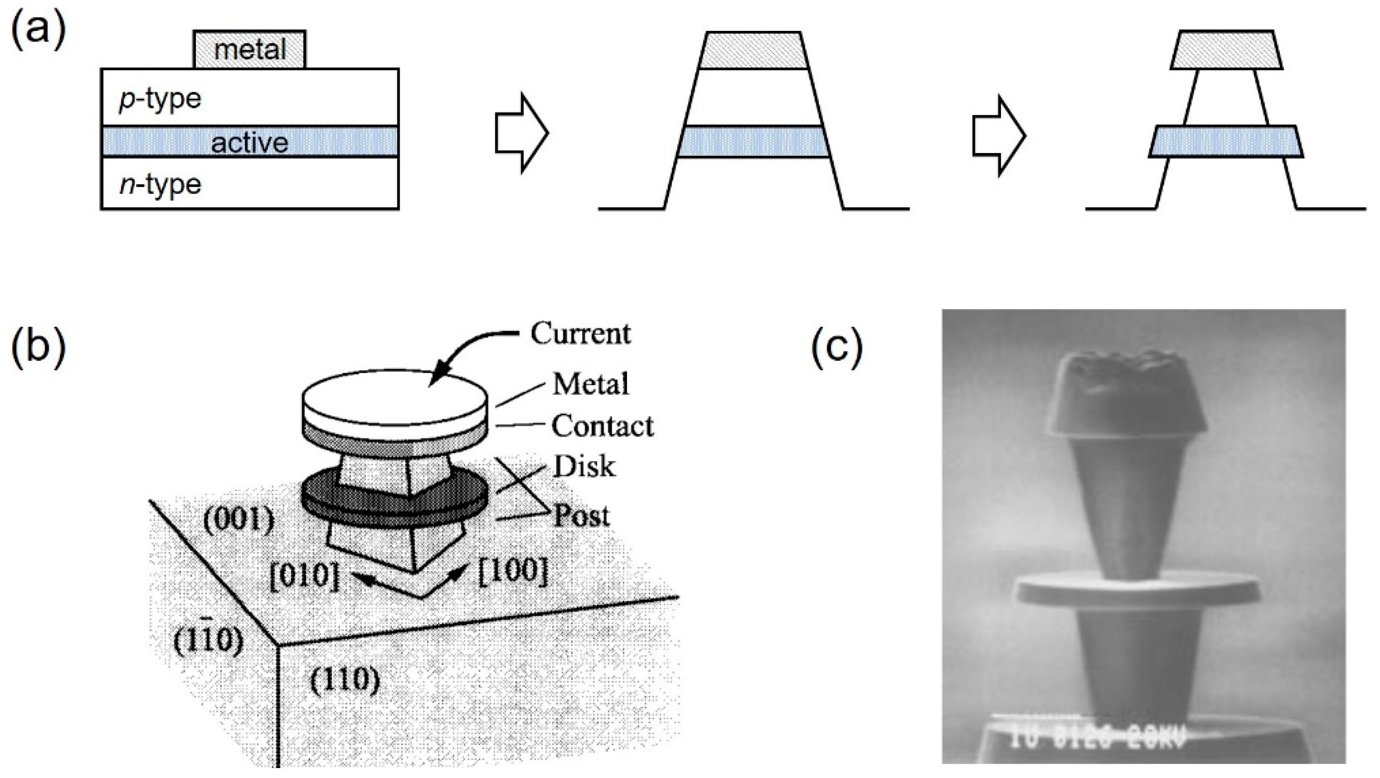
Figure 1a shows the key fabrication steps of current-injection microdisk cavity lasers. Circular metallic masks are lithographically defined on a vertically p-i-n-doped semiconductor wafer that contains an active medium in its intrinsic layer (left). Circular mesa structures with tilted sidewalls are formed after the conventional dry etching process (middle). A brief thermal treatment can be taken into account to make a good ohmic contact. The p-type top and n-type bottom layers are then selectively wet-etched, which results in a vertical micro-architecture consisting of a complex multileveled top-post/middle-microdisk/bottom-post structure. Here, due to the angled sidewalls from the dry etching process, the selective wet etching often gives rise to asymmetric top and bottom posts in size. Figure 1b illustrates a schematic overview of the laser device with a layered structure and current flow [13]. A sharp metallic probe directly injects pulsed or continuous-wave (CW) currents into the top metal electrode, which is connected to a highly p-doped contact layer. Carriers are injected into the active layer from the posts. The injected carriers diffuse from the center of the microdisk to the edge, where high-Q WGMs travel and repeat the total reflection at the semiconductor−air boundaries. When the WGMs acquire enough optical gain from the diffused carriers, and subsequent radiative recombination, strong lasing oscillations occur. Figure 1c shows a scanning electron microscope (SEM) image of the fabricated laser device exhibiting the InGaAs/InGaAsP microdisk, supported by the InP posts [12].
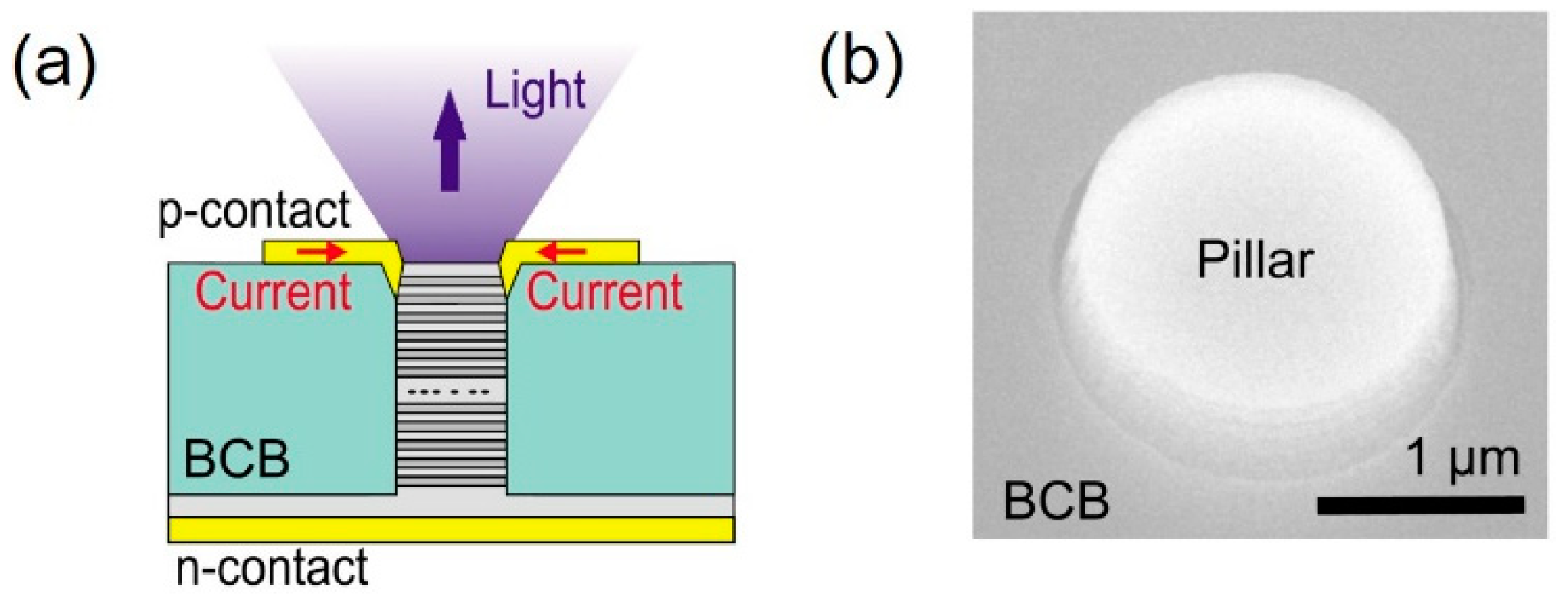
Semiconductor micropillars with embedded QDs have also proven to be very attractive structures for microscale injection light sources. In particular, when additional distributed Bragg reflector (DBR) structures are introduced to the micropillar, resembling minimized vertical-cavity surface emitting lasers, it serves as a high-Q microcavity with a more efficient collection of the emitted light and a better heat transfer compared to planar microdisk injection lasers [16,17]. Figure 2a illustrates a schematic view of the electrically pumped micropillar laser structure. Figure 2b shows the SEM image of the fabricated device before metallization [17]. The device comprises a p-doped upper DBR, an intrinsic one-λ-thick GaAs cavity layer, and an n-doped lower DBR. Here, the upper and lower DBRs are composed of multiple pairs of GaAs/AlAs layers. The QDs are placed at the center of the intrinsic layer. A key step in the fabrication that makes this structure distinguishable from other planar injection microlasers is the planarization using benzocyclobutene (BCB), a photosensitive polymer frequently used as a low-k dielectric in microelectronics packaging and interconnect applications [18]. This dielectric planarization serves as both a stable physical ground, on which the upper contact can be located, and an efficient electrical isolation layer. In addition, the low-k nature minimizes the undesirable optical perturbation to the micropillar cavities. Using the BCB layer, the electrical current can be injected through the upper p-contact and generate electron-hole pairs in the QD layer.
Since the first experimental observation of the pulsed-injection lasing, a series of intensive efforts have been made to demonstrate more practical injection microcavity lasers to achieve the best performance. For example, research efforts in reducing the size of the microdisk cavity down to a single-mode condition allowed for a significant decrease in threshold current from sub-mA to a few hundred μA [12]. A rational design based on the systematic theoretical analysis of scattering loss, by post and carrier diffusion in the active medium, enabled the CW lasing operation at room temperature [13,19]. Moreover, an improved dry etching technique helped to form vertical sidewalls in the microcavity, as well as symmetric top and bottom posts, which led to a further reduction in the lasing threshold [14]. Micropillar cavity lasers benefited from BCB planarization and the optimized ring-shaped upper contact scheme, facilitating the demonstration of strong lasing oscillations associated with lasing threshold currents as low as few μA at cryogenic temperature [16]. These high-Q and electrically pumped microcavities, besides their practical purposes, have been extensively exploited with respect to the influence of cavity quantum electrodynamic (cavity-QED) effects on the lasing properties, controlling the spontaneous emission and reducing the lasing threshold toward the ultimate laser with no threshold [13,15].
3. Electrically Driven Photonic Crystal (PhC) Nanocavity Lasers
The development of miniaturized semiconductor lasers, with high beam quality and low threshold with minimum thermal overload, is one of the essential goals for the realization of compact integrated photonic circuits [20]. For more than a decade, PhCs, an artificial structure whose refractive index is periodically modulated with sub-micrometer periodicity, have served as the most powerful platform to achieve this goal [21]. In particular, a two-dimensional (2D) semiconductor PhC slab structure has attracted tremendous interest, owing to its critical advantages. First, it can be readily realized by the conventional semiconductor crystal growth and fabrication technologies. The introduction of a sacrificial layer to the semiconductor wafer and definition of an array of air holes bring forth the air-suspended slab structure with periodic air–semiconductor index modulation. Second, light can be tightly confined inside the slab by total internal reflection (TIR) in the vertical direction and photonic band gap (PBG) in the lateral direction. Third, there is considerable room for designing various PhCs and manipulating the behaviors of the confined light. These pronounced features allow for the realization of wavelength-scale optical nanocavities that support resonant optical modes with a high-Q factor and small mode volume. Consequently, the PhC nanocavity lasers exhibit an ultrasmall device footprint and operate with a very low threshold. In addition, cavity engineering provides access to control important beam qualities (e.g., polarization state and spatial emission pattern) as well as device functionalities.
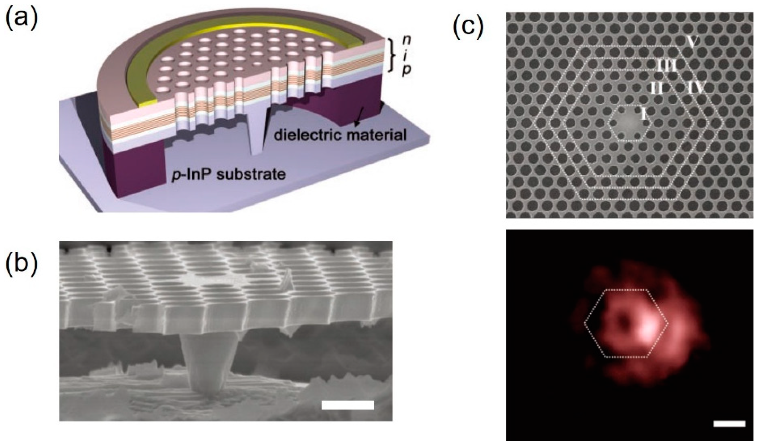
Considerable efforts have been made to put forth various cavity designs, characterize lasing properties, reduce various optical losses, and optimize device performance. However, the lasing operation from wavelength-scale optical cavities by direct electrical pumping has remained challenging. Because of such a small physical footprint, constructing a robust pathway through which the carriers can flow is a limitation. In addition, the confinement of carriers and photons should be achieved simultaneously. The injected carriers should be recombined in the vicinity of the nanocavity without seriously degrading the optical properties of resonant modes. All of these require extra consideration in the cavity design. Park et al. (2004) reported an electrically driven 2D PhC nanocavity laser that overcame the abovementioned limitations [22,23,24]. Figure 3 shows a schematic illustration and a tilted SEM image of the electrically driven single-cell PhC nanocavity. The 2D PhC pattern in a triangular-lattice fashion was introduced to an air-suspended and vertically n-i-p-doped InGaAsP slab containing an MQW structure. The nanocavity was a single air hole. Here, the authors judiciously modified the single-cell cavity by reducing the nearest air holes and slightly pushing them outward. This modification enlarged the cavity area and helped the InP sacrificial layer to survive after time-controlled wet-etching, which enables the introduction of a sub-micrometer central post underneath the cavity. The electrons and holes were supplied by the n-type electrical contact, defined at a distance from the PhC pattern and the p-doped InP post, respectively. A rich radiative recombination occurred near the post, and most of the generated photons were successfully confined within the nanocavity. Single-mode lasing oscillation with an estimated Q-factor of >2500 was observed at a low threshold current of ~260 μA. In a series of follow-up studies from the same group, the cavity design was further improved with the help of an extensive mode analysis using the 3D finite-difference time-domain (FDTD) method and the controlled low-temperature wet-etching technique [23,24,25]. As a result, a significant reduction in the threshold current, down to ~100 μA, was successfully achieved.
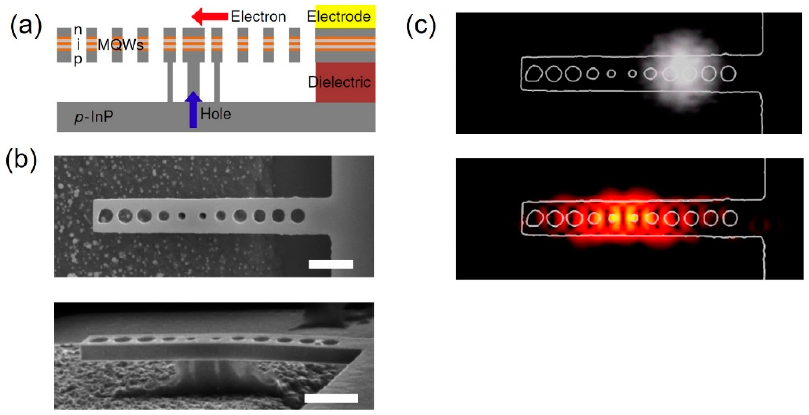
Taking advantage of the current injection scheme through a sub-micrometer-sized central post, even nanocavities smaller than 2D PhC nanocavities became a realistic candidate for an electrically pumped nanolaser. In the late 2000s, a 1D PhC structure, called a nanobeam, was extensively explored for ultrahigh-Q optical nanocavities with ultimately small physical and mode volumes [26,27,28]. These cavities strongly confine photons using PBG in the axial direction and TIR in both vertical and lateral directions, which often exhibit Q-factors > ~106 and mode volumes < (λ/2n)3. Among the numerous designs of ultrahigh-Q nanobeam cavities, the L0 nanobeam cavity (i.e., zero missing air holes) with graded air-hole sizes was employed to demonstrate the smallest possible nanolaser [29]. Figure 4a shows the schematic of the cross-sectional view of the laser device that exhibits the carrier injection paths. In Figure 4b, the top and tilted SEM images of the fully fabricated device show the L0 nanobeam nanocavity consisting of eleven air holes. The physical volume of the device was surprisingly small, i.e., ~4.6 × 0.61 × 0.28 μm3. The central posts supported the entire laser device. However, the lasing action was observed at a threshold current of ~650 μA at room temperature, which was not as low as expected considering the reduced physical size. The major factors that determined the threshold current were the large surface recombination losses, the weakened PBG confinement due to the limited number of air holes, as well as the increased thermal overload from the sub-micrometer-sized posts. Indeed, the L3 nanobeam cavity (i.e., three missing air holes) laser, with the enlarged post and the increased number of air holes, revealed that a larger size of the cavity structure helped in reducing the lasing threshold. The authors reported a measured threshold current of ~5 μA at room temperature, claiming a record threshold value among the electrically driven metal-free nanolasers at room temperature.
4. Lateral Injection PhC Nanocavity Lasers and Light-Emitting Diodes (LED) Modulators
Despite the successful demonstrations of the electrically driven lasing operation in some PhC nanocavities, the vertical carrier injection scheme through the p-i-n (or n-i-p)-doped PhC slab with a thickness of a few hundred nanometers still has limitations. For example, the central post structure requires complicated fabrication, including a precise, time-controlled undercut step [22,23,24,25,29]. In addition, the cavity design for the current injection is limited because the size and position of the air holes critically determines the formation of the sub-micrometer-sized post. This diminishes one of the key advantages of using PhCs: controlling the laser beam quality by cavity engineering. Moreover, the central post is located right underneath the nanocavity, so the leakage of carriers and photons is unavoidable, which can be a major factor for the increased threshold and thermal overload in lasing action. On the other hand, the vertical carrier injection scheme in nanocavities without the central post often suffered from the limited current spreading due to thin conductive layers in the PhC membrane, which gave rise to an inefficient cavity-coupled electroluminescence (EL) [30].
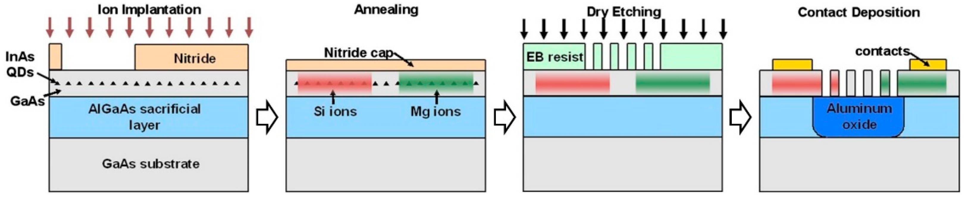
The researchers at Stanford proposed an alternative scheme to address these issues and electrically pumped arbitrary PhC nanocavities. Ellis et al. (2010) developed a technique to form a lateral p-i-n junction in a 2D PhC nanocavity by employing the ion implantation technique, a standard method of doping in the electronics industry [31]. Figure 5 describes the important fabrication steps of the lateral current injection PhC nanocavity. First, a nitride mask is lithographically defined on top of the GaAs membrane, where a high-density single InAs QD layer is included in the middle. Second, Si and Mg ions are separately implanted on the targeted areas. These dopants are subsequently capped by a nitride layer and activated by high-temperature annealing. Third, a PhC pattern is defined in a resist and transferred into the GaAs membrane by dry etching. To form a lateral p-i-n junction, the upper and lower sections of the PhC pattern are precisely aligned to the upper p- and lower n-doped regions, while the nanocavity is aligned to the middle intrinsic region. Finally, the n- and p-type contacts are metallized after the AlGaAs sacrificial layer is oxidized. With this technique, the authors successfully injected electrical current through the nanocavity and observed a cavity EL peak at low temperature, but failed to observe the lasing action due to the insufficient optical gain needed for amplified stimulated emission.
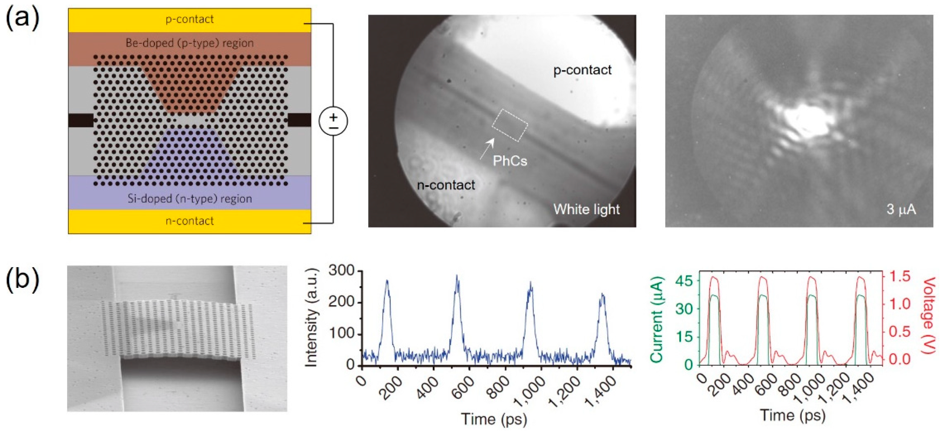
Additional improvements in doping density, dopant material, number of QD layers, and cavity fabrication allow for a successful demonstration of an ultralow threshold lasing action from a 2D QD PhC nanocavity [32]. A schematic diagram in Figure 6a shows the upper Be-doped (p-type), middle undoped (intrinsic), and lower Si-doped (n-type) PhC regions, forming a lateral p-i-n junction on the sub-micron scale. A bright-field IR camera image displays a PhC pattern between the p- and n-contacts. Strong lasing oscillation at a pump current of only 3 μA demonstrated an ultralow-threshold current nanolaser. Indeed, the reported threshold currents of the device were only 181 nA at 50 K and 287 nA at 150 K, claiming to be the lowest thresholds in any type of electrically pumped laser. The same device platform was exploited again to demonstrate ultrafast optical modulation (Figure 6b) [33]. Due to the insufficient QD gain at room temperature, the device no longer worked as a nanolaser, but operated as a nanoscale single-mode LED (nano-LED). In particular, the nano-LEDs benefitted from the sub-micrometer-sized lateral p-i-n junction with an extremely small capacitance and exhibited the capability of ultra-fast electrical switching at a speed of several GHz. As a result, the nano-LED device showed a modulation speed of up to ~10 GHz, which was an order of magnitude faster than that in the previous solutions.
Despite the many structural advantages, the lateral current injection scheme still has several limitations to be a practical solution. First, the implantation process causes inevitable damage to the semiconductor crystals and sacrifices the optical gain. Therefore, the process requires a precise control over the dopant density to strike a fine balance between sufficient carrier injection and reduction in optical gain. Second, the device fabrication includes multiple rounds of electron beam lithography with nanoscale precision and accuracy. In particular, the definition of the PhC pattern, with the nanocavity exactly aligned to the intrinsic region of the implanted wafer, is the most critical step that determines the successful formation of the junction. Third, the achieved lasing demonstrations at cryogenic temperatures have been limited. To be a practical light source in an integrated circuit, a laser device should operate at room temperature. This naturally requires a direct application of the scheme in typically used active materials at room temperature (e.g., QWs).
5. Nanowires (NW)-Based Electrically Driven Light Sources
Planar semiconductor growth technologies allow for the mass production of high-quality crystals with precisely controlled energy band structures. In addition, well-developed semiconductor microprocessing enables a robust and reproducible fabrication of electrically driven, active photonic devices. However, the sophisticated device structures associated with multiple junctions and bandgap engineering, and the high cost of device fabrication, make these light sources difficult to be integrated directly with other technologies such as silicon-based electronics, photonics, and micromechanical platforms. To address these issues for integrated applications, various active organic/inorganic materials and nanostructures have been transformed into devices, testing feasibility of achieving high-quality light generation [34,35,36,37]. In particular, rapid advancement in synthesizing 1D nanomaterials with controlled sizes and tunable electrical and optical properties has accelerated the development of electrically driven light sources [36,37].
Single-crystal semiconductor NWs exhibit several features that render them very attractive for optoelectronic devices. First, the semiconductors used for synthesizing NWs represent a high index of refraction in a broad range of optical frequencies. As a result, the single-NW functions as a stand-alone Fabry–Perot optical cavity and gain medium. Second, the high crystallinity ensures defect-free structures that guarantee both superior electrical transport and strong photon confinement. Third, the precise synthetic control allows for the rational design of electronic band structures, which enables the broadband tunability of central emission wavelengths.
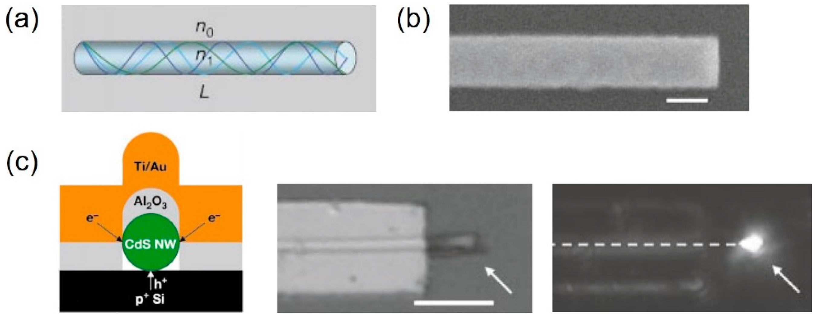
The first demonstration of an electrical injection single NW laser is shown in Figure 7 [36]. Single-crystal n-type CdS NW optical cavities are registered onto p-Si electrodes defined in heavily p-doped planar substrates. This hybrid structure forms an n-CdS/p-Si hetero-junction, which provides a channel through which the carriers can flow. After the electrical isolation by Al2O3 and n-type electrode metallization, the electrons and holes are injected along the entire length of the CdS NW. Bright-field optical microscope image shows a fully fabricated, single NW laser device. A strong EL emission at the NW end was observed at an injection current of 80 μA (below threshold). The device exhibited evident signatures of lasing oscillation (e.g., superlinear increase in output intensity vs. input current, abrupt linewidth reduction) at an injection current >200 μA. However, the lasing operation at levels substantially above threshold was limited due to the non-uniformity of carrier injection originating from the non-ideal n-Cd/p-Si junction, making it difficult to determine the clear threshold current.
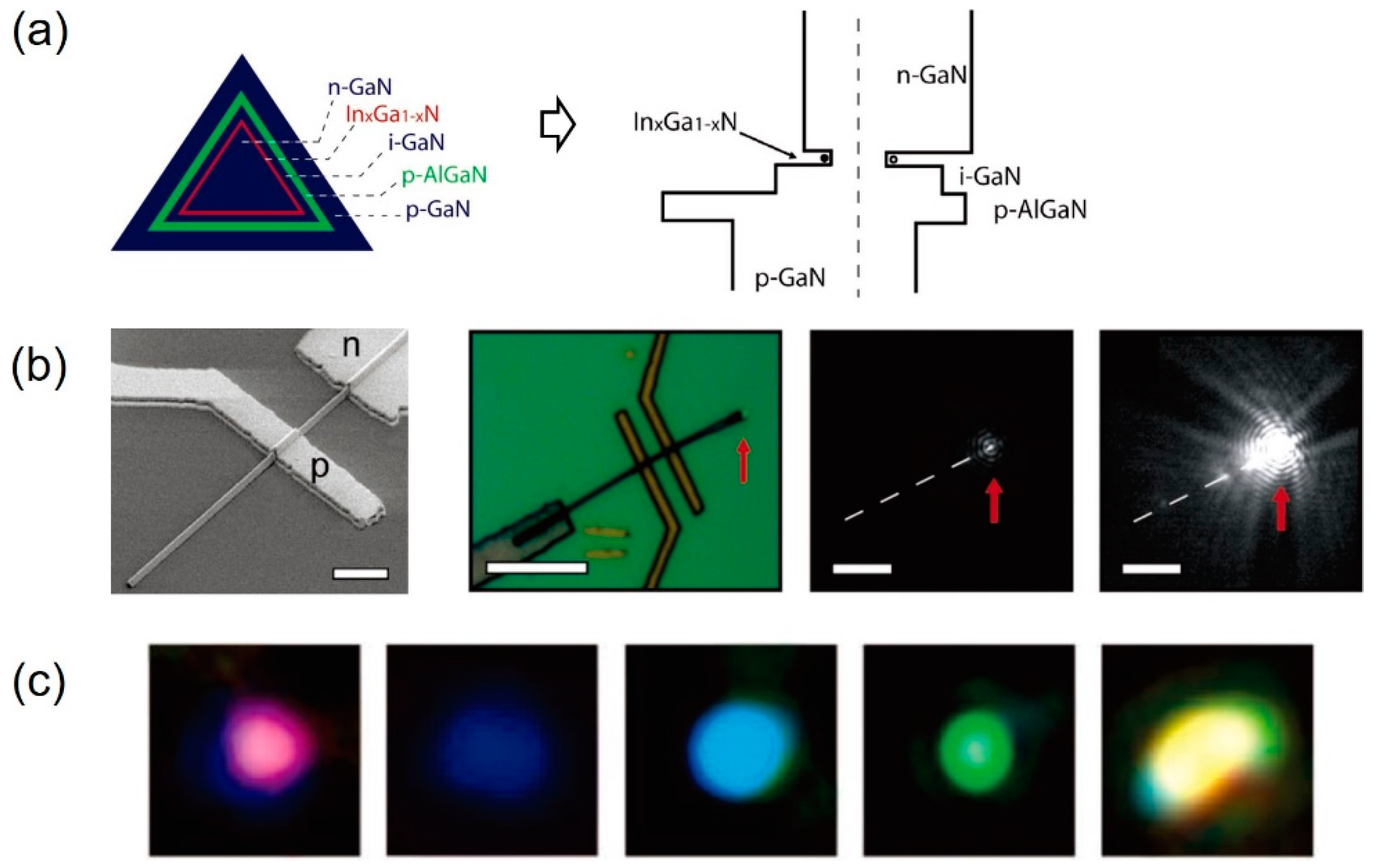
Tuning of the emission wavelength of single NWs in a broad range of optical frequencies has been successfully demonstrated by exploring advanced material growth technologies. Researchers at Harvard have reported various n-i-p core/multishell single NW heterostructures [37]. Figure 8a schematically shows the triangular cross section of a single GaN-based heterostructure, comprising a n-GaN core and an InxGa1−xN/GaN/p-AlGaN/p-GaN shell. Here, the InxGa1−xN layer provides a tunable band gap well, allowing systematic redshift of the emission peak with an increasing In composition. In Figure 8b, the separately deposited metal contacts onto the n-GaN core and p-GaN shell forms a stable injection path for single NW LEDs. Multicolor emissions in the visible frequency range were observed with various In compositions (Figure 8c: purple (1%), blue (10%), green (25%), and yellow (35%)). Notably, at a high forward bias of 11 V, a dominant light emission at the NW end was observed, indicating that a considerable amount of the generated light was coupled to NW waveguide modes. The result represents the potential of stimulated emission at higher current injection, eventually demonstrating an electrically driven single GaN NW laser.
6. Electrically Pumped Metal Nanocavity Lasers
Semiconductor-based optical devices and their integrated circuits are fundamentally limited in terms of their sizes because the diffraction of light plays a dominant role when the size of an optical device becomes comparable to, or smaller than, the wavelength of light in the material. Surface plasmon polaritons (SPPs), surface-bound electromagnetic waves supported by the metal dielectric interface, can offer an exclusive solution that addresses the diffraction of light by concentrating electromagnetic fields in nanoscale regions that are far smaller than the wavelength of the material [38]. For more than a decade, researchers have made tremendous efforts to propose new designs of essential plasmonic elements, and they have experimentally demonstrated the feasibility of their respective functions [39]. In particular, plasmonic light sources, together with other key components including plasmonic waveguides, modulators, and detectors, have been the mainstream research of nanophotonics. However, despite the numerous investigations on the optical properties of plasmonic nanocavities, the realization of an electrically driven plasmonic source remains a great challenge because there have been limited schemes satisfying the conditions for simultaneous carrier injection, SPP generation, and confinement with minimized ohmic loss in a subwavelength volume.
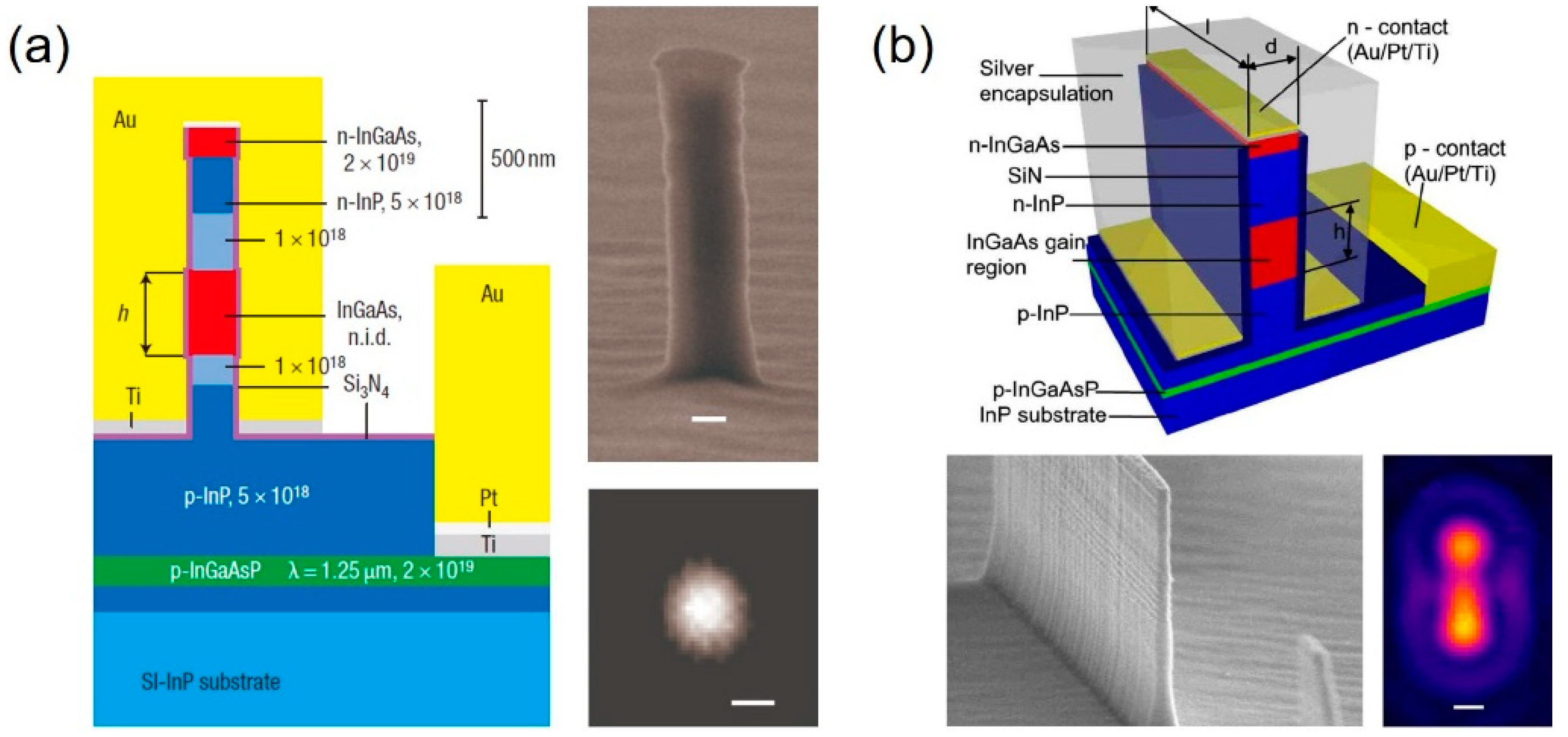
To circumvent these difficulties, several strategies have been proposed. For example, the metal encapsulation of a vertical semiconductor nanostructure is a successful scheme [40,41]. Figure 9a shows the first electrically driven metal cavity nanolaser, the gold-finger nanocavity laser [40]. The nanocavity comprises an inner n-InP/i-InGaAs/p-InP heterostructure vertical nanopillar, a thin nitride isolation layer on the sides of the pillar, and an outer gold cavity encapsulating the entire semiconductor/insulator structure. The vertically injected carriers are recombined in the intrinsic InGaAs region where a slight index contrast between InP and InGaAs allows for a resonant cavity mode. In the experiment, lasing oscillations were observed at low-threshold currents of 3.5 and 6.0 μA at cryogenic temperatures of 10 and 77 K, respectively. However, lasing operation failed at room temperature due to the increased metallic loss, reduced material gain, and decreased Q-factor. In this study, the author did not specifically identify the origins of the observed lasing modes (e.g., plasmonic or photonic lasing mode). It remains questionable whether it is the first electrically driven plasmonic laser, although it is clearly the first metallic nanocavity nanolaser. In their follow-up paper, the same authors reported modified cavity structures and realized plasmonic lasing [41]. In Figure 9b, the rectangular semiconductor active core with a length of few μm (indicated as l) is employed. This plasmonic waveguide cavity supports Fabry–Perot-type resonant modes in the axial direction. In addition, the reduced width of 130 nm in the rectangular core (indicated as d) only allowed a transverse magnetic (TM) mode (or gap plasmon mode) in a deep sub-wavelength region. The optical microscope image shows the plasmonic lasing mode, revealing the subwavelength confinement of SPPs. The lasing threshold current was measured as ~40 μA at a low temperature of 78 K, which was an order of magnitude higher than that of the gold-finger nanocavity laser. It is believed that the increased metal/insulator or metal/semiconductor interfaces, where the light−matter interaction strongly occurred, inevitably produced optical loss and increased the lasing threshold.
7. Metal-Waveguide-Integrated Nano-LEDs for Surface Plasmon Polariton (SPP) Sources
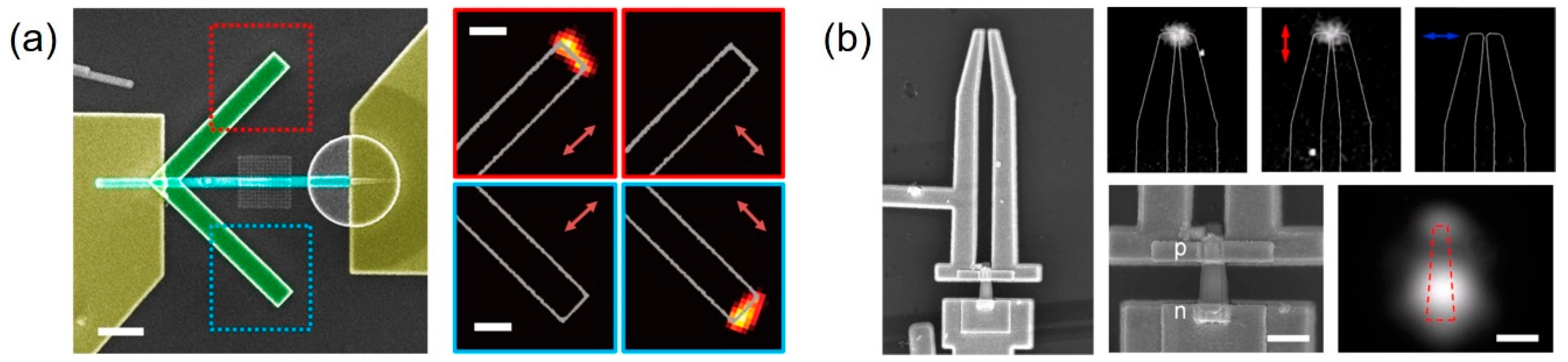
Another successful scheme for generating SPPs is coupling a light-emitting nanomaterial to passive plasmonic components [42,43]. In this scheme, the nanomaterial is electrically doped and forms a spatially localized p-n or p-i-n junction so that it can serve as a current-injectable nanoscale LED. A passive plasmonic component, such as a metal waveguide, is then coupled to the nano-LED in such a way that a major portion of the generated photons can interact with bound charges in metal. This process naturally helps to convert the photons into SPPs. Representative examples are shown in Figure 10. In Figure 10a, a bottom-up synthesized core-shell GaAs NW with a radial p-i-n junction is connected to n- and p-type contacts [42]. Two metallic strip waveguides, making a right-angle to each other at their ends, are coupled to the NW LED by covering the junction area where the carrier recombination and light generation occur. When the NW LED was electrically pumped, linearly polarized light emission parallel to the direction of each waveguide was observed at the end of the waveguide, which is a clear demonstration of electrically driven SPP generation and its propagation.
Top-down fabricated active nanomaterials can also be employed for nano-LEDs, provided that the materials are properly pumped through current injection [43]. The SEM images in Figure 10b show that a top-down fabricated GaAs NW with a vertical p-n junction is connected to metal contacts. One of the contacts (p-contact) is connected with two individual metal strips. While the NW is located at the center of the two ends of the strips, the coupled metal strips extend along the direction of the NW axis and form a double-strip plasmonic waveguide. Since the waveguide supports several propagating waveguide modes, the light emitted from the NW LED can couple to the modes and propagate. The polarization-dependent EL measurement, again, confirms the SPP generation and propagation. The metal-waveguide-integrated nano-LED, however, suffers from several limitations, mostly originating from the coupling geometry and ohmic loss. Since the SPP generation strongly depends on how efficiently the light from the nano-LED is coupled to the metal waveguide, the coupling geometry should be judiciously designed to maximize the interaction between the light and bound charges in metal. For example, the light coupling efficiency from the structures in Figure 10b was estimated at only few percentage points, which shows a clear limitation of such a scheme. In addition, the passive plasmonic components should support various plasmonic modes to which the light can couple, but at the same time, they should be designed to minimize the metallic loss. These two requirements are often contradictory to each other because increasing the size of the plasmonic waveguide can not only increase the number of plasmonic modes, but also cause more metallic loss. Furthermore, when the p- and n-type metal contacts are defined for the nanomaterial, they should minimally disturb the plasmonic waveguide structure, which is not always straightforward in many nanodevices.
8. Integration of Electrically Driven Light Sources with Silicon-On-Insulator (SOI) Photonic Circuits
Based on the electrical excitation schemes, we have reviewed various micro- and nano-scale optical and/or plasmonic light sources at a single device level. The research on these devices naturally indicates the next logical step: coupling to, or integration with, other optical components. Indeed, one can find a truly practical usefulness of these devices only if they are efficiently integrated with other passive components, and only if they properly serve as robust light sources in a photonic circuit that is designed to complete a desired function. To this end, finding a good passive photonic platform that eases the integration with low optical loss becomes critical. Among others, silicon-on-insulator (SOI) has been considered as one of the most promising platforms [44,45,46,47]. The high index of refraction can tightly confine the light, resulting in low optical leakage. In addition, silicon is transparent at telecommunication wavelengths. Importantly, the SOI platform can share the mature technological advances of the complementary metal oxide semiconductor (CMOS) industry. In particular, this CMOS compatibility can guarantee large-scale fabrication processing, and consequently, electronic−photonic integration.
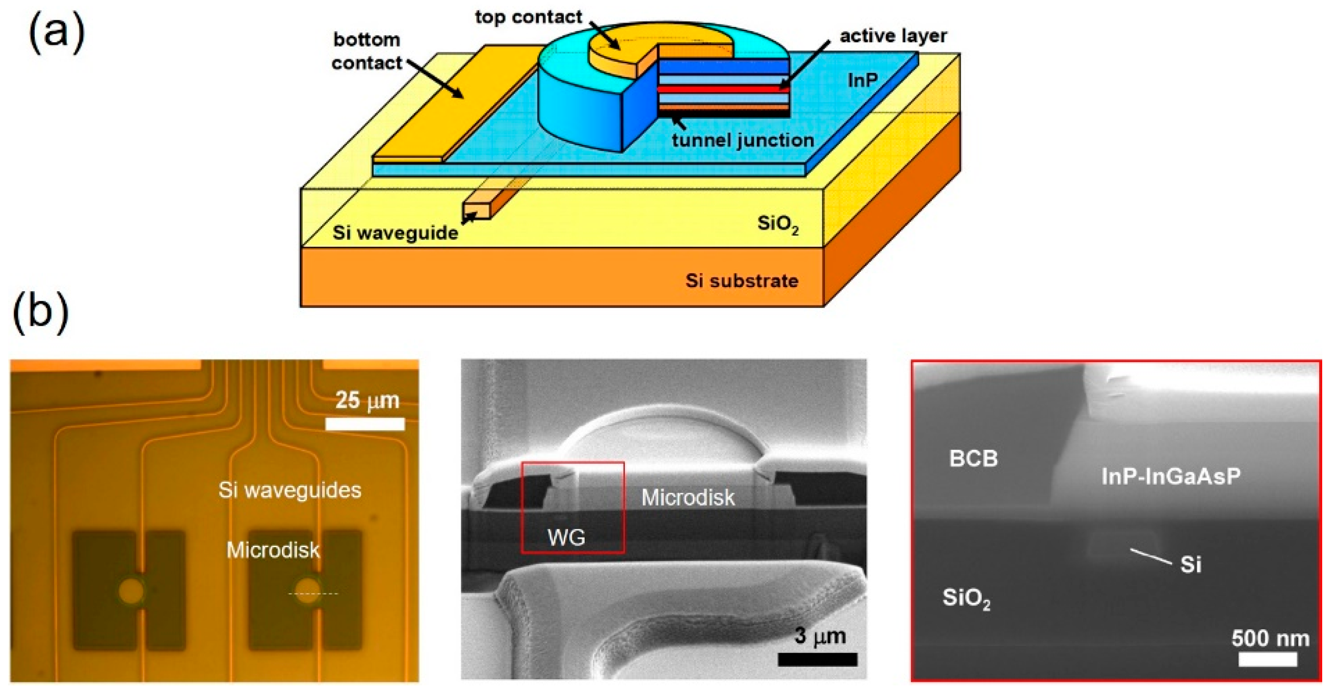
The heterogeneous integration shown in Figure 11 has been a successful solution [47]. The integration takes several key fabrication steps. First, current-injectable InP-based microdisk lasers were separately fabricated in a thin epilayer, while passive SOI waveguide circuits were fabricated using COMS processes. Second, after depositing SiO2, the SOI wafer was planarized by chemical–mechanical polishing until the targeted thickness of the deposited SiO2 was reached. Third, the laser devices in the thin epilayer were vertically aligned to, and integrated with, the waveguides in the SOI wafer through the wafer-bonding technique. In 2007, J. Van Campenhout et al. used this method, and reported the successful integration of electrically pumped microdisk lasers onto SOI waveguide circuits [47]. Figure 11a shows the top and cross-sectional views of optical and SEM images of the integrated device, revealing the details of layer configurations. In this device, light is primarily confined in the InP-based microdisk cavity, while a portion of it is evanescently coupled to the SOI waveguides. The microdisk laser with a threshold current of 0.5 mA was operated under the CW condition at room temperature. From the output power spectrum at the end of the SOI waveguide, the estimated slope efficiency just above the threshold was ~30 μW/mA, assuming a fiber coupler efficiency and propagation loss. These results represented the actual usefulness and practicality of the electrically driven microdisk lasers in a photonic circuit.
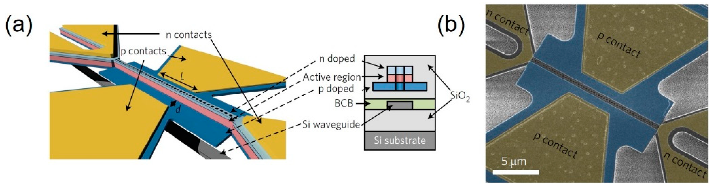
For more practical and power-efficient applications, researchers have applied this integration method to even smaller optical cavities, such as PhC nanocavities [48,49,50]. Crosnier et al. (2017) reported a highly power-efficient hybrid InP-based nanolaser diode (Figure 12) [50]. They employed an electrically driven InP-based 1D PhC nanocavity and integrated it in an SOI waveguide. They achieved electrically pumped CW lasing at room-temperature. Notably, the threshold current was measured as ~100 μA at 1 V applied voltage, which was five-fold lower than that of the microdisk laser in Figure 11. In addition, the reported device exhibited a maximum output power of ~95 μW, coupled in the SOI waveguide, and an estimated wall-plug efficiency of up to ~14%. Evidently, these results represent considerable improvements in many aspects of device performance compared to the previously reported electrically powered micro- and/or nano-scale lasers.
Two major challenges are worth mentioning for this heterogeneous integration. First, a simple and easy alignment with high precision and accuracy still need to be improved since the success of integration critically relies on this process. Second, the EM energy transfer is critically determined by how strongly or weakly the evanescent fields are formed between the laser and waveguide. Therefore, finding an optimal thickness of the deposited and planarized SiO2 layer is of considerable importance.
9. Electrically Pumped Plasmonic Light Sources and Optical Nanocircuits
The integration of multiple optical elements is fundamentally size-limited because the size of each optical component is diffraction-limited. In addition, the light interaction between the optical elements requires a minimum coupling length that is sometimes a few-fold larger than the wavelength of light. The heterogeneous integration, therefore, is suitable for optical circuits whose sizes are larger than a few mm2 or cm2, and is limited for highly dense nanoscale circuits. Indeed, an ultracompact optical nanocircuit requires subwavelength-scale photonic elements and their integration at nanoscale precision. Plasmonic integrated circuits can be a promising solution for this purpose. The key plasmonic elements such as light sources, waveguides, and couplers can be fabricated at deep subwavelength scale. The plasmonic interaction between these elements occurs in a truly nanoscale regime, allowing high density of integration in an extremely small physical volume.
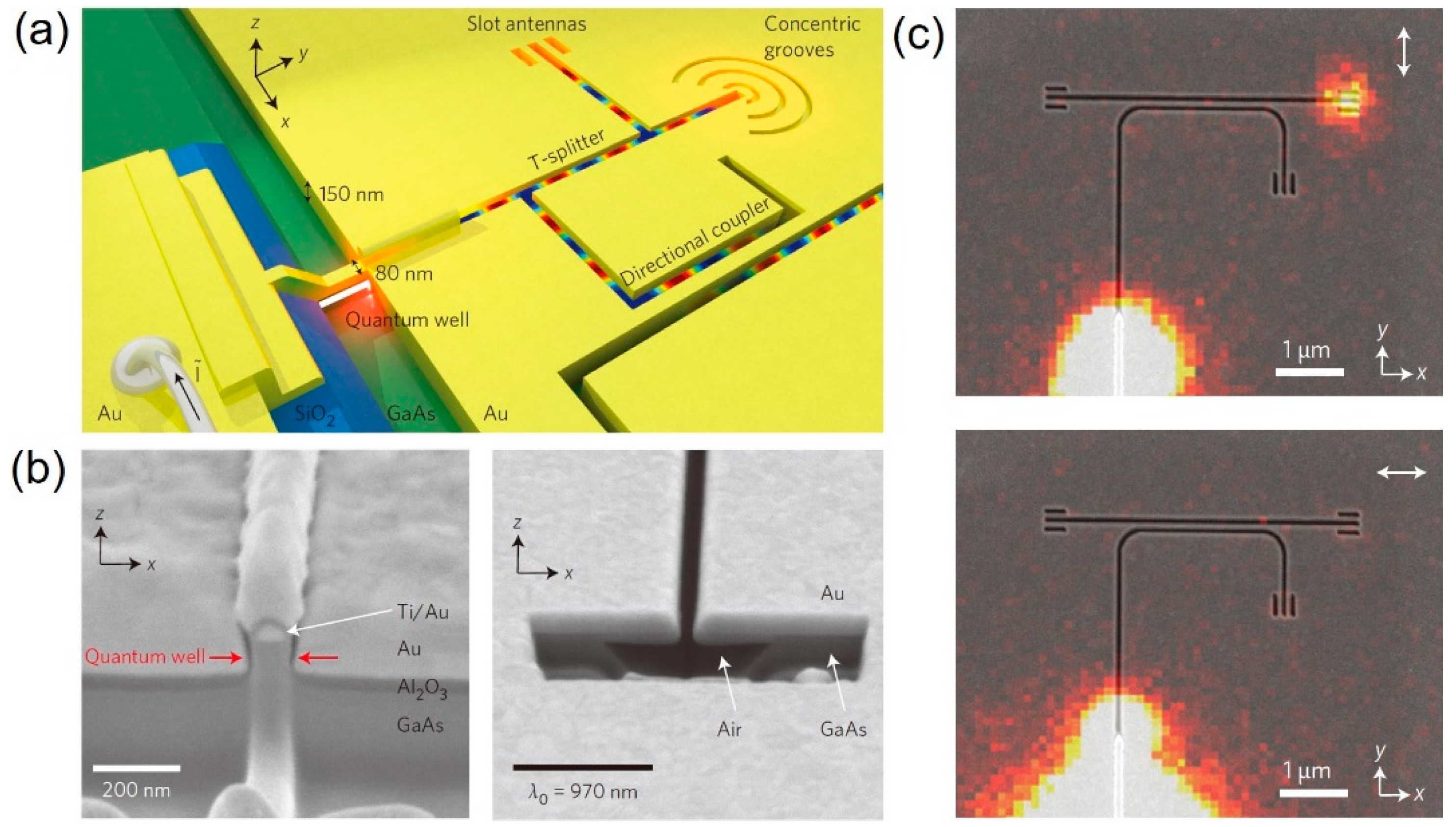
There has been considerable research on plasmonic integrated circuits [39]. However, electrical empowering is still a critical issue to be addressed. Recently, Huang et al. have succeeded in electrically empowering optical nanocircuits, comprising a nanoscale GaAs ridge LED that was coupled to subwavelength-sized metal-slot waveguides [51]. Figure 13 shows a schematic of the plasmonic circuit. The SEM images exhibit cross-sectional views of a 130 nm-tall and 60 nm-wide GaAs ride LED, and a 150 nm-tall and 80 nm-wide slot waveguides, revealing truly subwavelength-scale individual circuit components. The authors demonstrated the electrical generation of SPPs, coupling them to a propagating plasmonic waveguide mode, performing 90° light splitting in a T-splitter, and coupling to another slot waveguide in a plasmonic directional coupler. All these circuits were fabricated on the order of a few μm2, which is difficult to achieve in conventional optical circuits.
10. Summary
This paper provides a comprehensive overview of the electrically pumped, micro- and nano-scale optical cavity-based semiconductor light sources. It describes the basic mechanisms for electrical carrier injection and photon confinement. As new designs of high-Q semiconductor optical cavities are proposed, high-performance and power-efficient lasers and LEDs are further developed. Their application in photonic circuits is already being demonstrated in many research areas, but is still far from a fully integrated photonic circuit that can perform its function in actual optoelectronic devices. A remaining challenge to be addressed in the near future is the development of an optimal integration method that can enable compact, high-density, and heterogeneous integration of various optical components in a single chip.
Funding
This work was supported by the Basic Science Program of the National Research Foundation of Korea (NRF) funded by the Ministry of Education (2018R1C1B3001130).
Conflicts of Interest
The authors declare no conflict of interest.
References
- Gramotnev, D.K.; Bozhevolnyi, S.I. Plasmonics beyond the diffraction limit. Nat. Photonics 2010, 4, 83–91. [Google Scholar] [CrossRef]
- Reed, G.T.; Mashanovich, F.Y.; Gardes, F.Y.; Thompson, D.J. Silicon optical modulators. Nat. Photonics 2010, 4, 518–526. [Google Scholar] [CrossRef] [Green Version]
- Sun, Z.; Martinez, A.; Wang, F. Optical modulators with 2D layered materials. Nat. Photonics 2016, 10, 227–238. [Google Scholar] [CrossRef] [Green Version]
- Kakitsuka, T.; Matsuo, S. Current-injection Photonic-crystal Laser. NTT Tech. Rev. 2012, 10, 1–6. [Google Scholar]
- Vahala, K. Optical microcavities. Nature 2003, 424, 839–846. [Google Scholar] [CrossRef] [PubMed]
- Bogaerts, W.; Heyn, P.D.; Vaerenbergh, T.V.; Vos, D.K.; Selvaraja, S.K.; Claes, T.; Dumon, P.; Bienstman, P.; Thourhout, D.V.; Baets, R. Silicon microring resonators. Laser Photonics Rev. 2012, 6, 47–73. [Google Scholar] [CrossRef]
- Ma, R.-M.; Oulton, R.F. Applications of nanolasers. Nat. Nanotechnol. 2019, 14, 12–22. [Google Scholar] [CrossRef] [PubMed]
- Bachelard, N.; Andreasen, J.; Gigan, S.; Sebbah, P. Taming Random Lasers through Active Spatial Control of the Pump. Phys. Rev. Lett. 2012, 109, 033903. [Google Scholar] [CrossRef] [PubMed]
- Ge, L.; Malik, O.; Türeci, E. Enhancement of laser power-efficiency by control of spatial hole burning interactions. Nat. Photonics 2014, 8, 871–875. [Google Scholar] [CrossRef] [Green Version]
- Choi, J.-H.; Chang, S.; Kim, K.-H.; Choi, W.; Lee, S.-J.; Lee, J.M.; Hwang, M.-S.; Kim, J.; Jeong, S.; Seo, M.-K.; et al. Selective Pump Focusing on Individual Laser Modes in Microcavities. ACS Photonics 2018, 5, 2791–2798. [Google Scholar] [CrossRef]
- Levi, A.F.J.; Slusher, R.E.; McCall, S.L. Room temperature operation of microdisc lasers with submilliamp threshold current. Electron. Lett. 1992, 28, 1010–1012. [Google Scholar] [CrossRef]
- Baba, T.; Fujita, M.; Sakai, A.; Kihara, M.; Watanabe, R. Lasing Characteristics of GaInAsP-InP Strained Quantum-Well Microdisk Injection Lasers with Diameter of 2–10 μm. IEEE Photonics Technol. Lett. 1997, 9, 878–880. [Google Scholar] [CrossRef]
- Fujita, M.; Sakai, A.; Baba, T. Ultrasmall and Ultralow Threshold GaInAsP-InP Microdisk Injection Lasers: Design, Fabrication, Lasing Characteristics, and Spontaneous Emission Factor. IEEE J. Sel. Top. Quantum Electron. 1999, 5, 673–681. [Google Scholar] [CrossRef]
- Fujita, M.; Ushigome, R.; Baba, T. Continuous wave lasing in GaInAsP microdisk injection laser with threshold current of 40 μA. Electron. Lett. 2000, 36, 790–791. [Google Scholar] [CrossRef]
- Fujita, M.; Ushigome, R.; Baba, T. Large Spontaneous Emission Factor of 0.1 in a Microdisk Injection Laser. IEEE Photonics Technol. Lett. 2001, 13, 403–405. [Google Scholar] [CrossRef]
- Böckler, C.; Reitzenstein, S.; Kistner, C.; Debusmann, R.; Löffler, A.; Kida, T.; Höfling, S.; Forchel, A.; Grenouillet, L.; Claudon, J.; et al. Electrically driven high-Q quantum dot-micropillar cavities. Appl. Phys. Lett. 2008, 92, 091107. [Google Scholar] [CrossRef]
- Reitzenstein, S.; Heindel, T.; Kistner, C.; Rahimi-Iman, A.; Schneider, C.; Höfling, S.; Forchel, A. Low threshold electrically pumped quantum dot-micropillar lasers. Appl. Phys. Lett. 2008, 93, 061104. [Google Scholar] [CrossRef]
- Chan, K.C.; Teo, M.; Zhong, Z.W. Characterization of low-k benzocyclobutene dielectric thin film. Microelectron. Int. 2003, 20, 11–22. [Google Scholar] [CrossRef]
- Buus, J.; Danielsen, M. Carrier Diffusion and Higher Order Transversal Modes in Spectral Dynamics of the Semiconductor Laser. IEEE J. Quantum Electron. 1977, 13, 669–674. [Google Scholar] [CrossRef]
- Coldren, L.A.; Corzine, S.W. Diode Lasers and Photonic Integrated Circuits; John Wiley & Sons: New York, NY, USA, 1995; ISBN 0-471-11875-3. [Google Scholar]
- Joannopoulos, J.D.; Johnson, S.G.; Winn, J.N.; Meade, R.D. Photonic Crystals: Molding the Flow of Light, 2nd ed.; Princeton University Press: Princeton, NJ, USA, 2008; ISBN 978-0-691-12456-8. [Google Scholar]
- Park, H.-G.; Kim, S.-H.; Kwon, S.-H.; Ju, Y.-G.; Yang, J.-K.; Baek, J.-H.; Kim, S.-B.; Lee, Y.-H. Electrically driven single-cell photonic crystal laser. Science 2004, 305, 1444–1447. [Google Scholar] [CrossRef] [PubMed]
- Park, H.-G.; Kim, S.-H.; Seo, M.-K.; Ju, Y.-G.; Kim, S.-B.; Lee, Y.-H. Characteristics of electrically driven two-dimensional photonic crystal lasers. IEEE J. Quantum Electron. 2005, 41, 1131–1141. [Google Scholar] [CrossRef]
- Park, H.-G.; Seo, M.-G.; Kim, S.-H.; Lee, Y.-H. Electrically Pumped Photonic Crystal Nanolasers. Opt. Photonics News 2008, 19, 40–45. [Google Scholar] [CrossRef]
- Seo, M.-G.; Jeong, K.-Y.; Yang, J.-K.; Lee, Y.-H.; Park, H.-G.; Kim, S.-B. Low threshold current single-cell hexapole mode photonic crystal laser. Appl. Phys. Lett. 2007, 90, 171122. [Google Scholar] [CrossRef]
- McCutcheon, M.W.; Lončar, M. Design of a silicon nitride photonic crystal nanocavity with a Quality factor of one million for coupling to a diamond nanocrystal. Opt. Express 2008, 16, 19136–19145. [Google Scholar] [CrossRef] [PubMed]
- Deotare, P.B.; McCutcheon, M.W.; Frank, I.W.; Khan, M.; Lončar, M. High quality factor photonic crystal nanobeam cavities. Appl. Phys. Lett. 2009, 94, 121106. [Google Scholar] [CrossRef] [Green Version]
- Quan, Q.; Deotare, P.B.; Lončar, M. Photonic crystal nanobeam cavity strongly coupled to the feeding waveguide. Appl. Phys. Lett. 2010, 96, 203102. [Google Scholar] [CrossRef] [Green Version]
- Jeong, K.-Y.; No, Y.-S.; Hwang, Y.; Kim, K.S.; Seo, M.-K.; Park, H.-K.; Lee, Y.-H. Electrically driven nanobeam laser. Nat. Commun. 2013, 4, 2822. [Google Scholar] [CrossRef]
- Francardi, M.; Balet, L.; Gerardino, A.; Chauvin, N.; Bitauld, D.; Li, L.H.; Alloing, B.; Fiore, A. Enhanced spontaneous emission in a photonic-crystal light-emitting diode. Appl. Phys. Lett. 2008, 93, 143102. [Google Scholar] [CrossRef] [Green Version]
- Ellis, B.; Sarmiento, T.; Mayer, M.; Zhang, B.; Harris, J.; Haller, E.; Vučković, J. Electrically pumped photonic crystal nanocavity light sources using a laterally doped p-i-n junction. Appl. Phys. Lett. 2010, 96, 181103. [Google Scholar] [CrossRef]
- Ellis, B.; Mayer, M.A.; Shambat, G.; Sarmiento, T.; Harris, J.; Haller, E.E.; Vučković, J. Ultralow-threshold electrically pumped quantum-dot photonic-crystal nanocavity laser. Nat. Photonics 2011, 5, 297–300. [Google Scholar] [CrossRef]
- Shambat, G.; Ellis, B.; Majumdar, A.; Petykiewicz, J.; Mayer, M.A.; Sarmiento, T.; Harris, J.; Haller, E.E.; Vučković, J. Ultrafast direct modulation of a single-mode photonic crystal nanocavity light-emitting diode. Nat. Commun. 2011, 2, 539. [Google Scholar] [CrossRef] [PubMed] [Green Version]
- Kozlov, V.G.; Bulović, V.; Burrows, P.E.; Forrest, S.R. Laser action in organic semiconductor waveguide and double-heterostructure devices. Nature 1997, 389, 362–364. [Google Scholar] [CrossRef]
- Kazes, M.; Lewis, D.Y.; Ebenstein, Y.; Mokari, T.; Banin, U. Lasing from Semiconductor Quantum Rods in a Cylindrical Microcavity. Adv. Mater. 2002, 14, 317–321. [Google Scholar] [CrossRef]
- Duan, X.; Huang, Y.; Agarwal, R.; Lieber, C.M. Single-nanowire electrically driven lasers. Nature 2003, 421, 241–245. [Google Scholar] [CrossRef] [PubMed]
- Qian, F.; Gradečak, S.; Li, Y.; Wen, C.-Y.; Lieber, C.M. Core/Multishell Nanowire Heterostructures as Multicolor, High-Efficiency Light-Emitting Diodes. Nano Lett. 2005, 5, 2287–2291. [Google Scholar] [CrossRef] [PubMed]
- Barnes, W.L.; Dereux, A.; Ebbesen, T.W. Surface plasmon subwavelength optics. Nature 2003, 424, 824–830. [Google Scholar] [CrossRef] [PubMed]
- Fang, Y.; Sun, M. Nanoplasmonic waveguides: Towards applications in integrated nanophotonic circuits. Light Sci. Appl. 2015, 4, 294. [Google Scholar] [CrossRef]
- Hill, M.T.; Oei, Y.-S.; Smalbrugge, B.; Zhu, Y.; Vries, T.D.; Veldhoven, P.J.V.; Otten, F.W.M.V.; Eijkemans, T.J.; Turkiewicz, J.P.; Waardt, H.D.; et al. Lasing in metallic-coated nanocavities. Nat. Photonics 2007, 1, 589–594. [Google Scholar] [CrossRef]
- Hill, M.T.; Marell, M.; Leong, E.S.P.; Smalbrugge, B.; Zhu, Y.; Sun, M.; Veldhoven, P.J.V.; Geluk, E.J.; Karouta, F.; Oei, Y.-S.; et al. Lasing in metal-insulator-metal sub-wavelength plasmonic waveguides. Opt. Express 2009, 17, 11107–11112. [Google Scholar] [CrossRef] [PubMed]
- Fan, P.; Colombo, C.; Huang, K.C.Y.; Krogstrup, P.; Nygård, J.; Morral, A.F.I.; Brongersma, M.L. An Electrically-Driven GaAs Nanowire Surface Plasmon Source. Nano Lett. 2012, 12, 4943–4947. [Google Scholar] [CrossRef] [PubMed]
- No, Y.-S.; Choi, J.-H.; Ee, H.-S.; Hwang, M.-S.; Jeong, K.-Y.; Lee, E.-K.; Seo, M.-K.; Kwon, S.-H.; Park, H.-G. A Double-Strip Plasmonic Waveguide Coupled to an Electrically Driven Nanowire LED. Nano Lett. 2013, 13, 772–776. [Google Scholar] [CrossRef] [PubMed]
- Roelkens, G.; Thourhout, D.V.; Baets, R. Laser emission and photodetection in an InP/InGaAsP layer integrated on and coupled to a Silicon-on-Insulator waveguide circuit. Opt. Express 2006, 14, 8154–8159. [Google Scholar] [CrossRef] [PubMed]
- Fang, A.W.; Park, H.; Cohen, O.; Jones, R.; Paniccia, M.J.; Bowers, J.E. Electrically pumped hybrid AlGaInAs-silicon evanescent laser. Opt. Express 2006, 14, 9203–9210. [Google Scholar] [CrossRef] [PubMed]
- Fang, A.W.; Jones, R.; Park, H.; Cohen, O.; Raday, O.; Paniccia, M.J.; Bowers, J.E. Integrated AlGaInAs-silicon evanescent racetrack laser and photodetector. Opt. Express 2007, 15, 2315–2322. [Google Scholar] [CrossRef] [PubMed]
- Campenhout, J.V.; Rojo-Romeo, P.; Regreny, P.; Seassal, C.; Thourhout, D.V.; Verstuyft, S.; Cioccio, L.D.; Fedeli, J.-M.; Lagahe, C.; Baets, R. Electrically pumped InP-based microdisk lasers integrated with a nanophotonic silicon-on-insulator waveguide circuit. Opt. Express 2007, 15, 6744–6749. [Google Scholar] [CrossRef] [PubMed]
- Karle, T.J.; Halioua, Y.; Raineri, F.; Monnier, P.; Braive, R.; Gratiet, L.L.; Beaudoin, G.; Sagnes, I.; Roelkens, G.; Laere, F.V.; et al. Heterogenous integration and precise alignment of InP-based photonic crystal lasers to complementary metal-oxide semiconductor fabricated silicon-on-insulator wire waveguides. J. Appl. Phys. 2010, 107, 063103. [Google Scholar] [CrossRef]
- Crosnier, G.; Sanchez, D.; Bazin, A.; Monnier, P.; Bouchoule, S.; Braive, R.; Beaudoin, G.; Sagnes, I.; Raj, R.; Raineri, F. High Q factor InP photonic crystal nanobeam cavities on silicon wire waveguides. Opt. Lett. 2016, 41, 579–582. [Google Scholar] [CrossRef] [PubMed]
- Crosnier, G.; Sanchez, D.; Bouchoule, S.; Monnier, P.; Beaudoin, G.; Sagnes, I.; Raj, R.; Raineri, F. Hybrid indium phosphide-on-silicon nanolaser diode. Nat. Photonics 2017, 11, 297–300. [Google Scholar] [CrossRef]
- Huang, K.C.Y.; Seo, M.-K.; Sarmiento, T.; Huo, Y.; Harris, J.S.; Brongersma, M.L. Electrically driven subwavelength optical nanocircuits. Nat. Photonics 2014, 8, 244–249. [Google Scholar] [CrossRef]
Figure 1.
Current injection microdisk lasers: (a) Schematics of the key fabrication steps for an injection microdisk structure; electron-beam lithographic definition of circular metal masks on a vertically p-i-n-doped semiconductor wafer where the active medium is included in the middle (left); formation of circular mesas with tilted sidewalls after applying chemically assisted dry etching (middle); and final microdisk structure with asymmetric n- and p-type posts after the wet etching process. (b) Schematic of InGaAsP microdisk injection laser. The microdisk is supported by top and bottom InP posts connected to the top Ti/Au contact and bottom p-type InP substrate [13]. Figure reproduced with permission from the Institute of Electrical and Electronics Engineers. (c) SEM image of the fabricated injection microdisk laser [12]. Figure reproduced with permission from the Institute of Electrical and Electronics Engineers.

Figure 2.
Current injection micropillar lasers. (a) Schematic of the electrically driven quantum dot (QD)-micropillar laser structure (left). The cavity layer where QDs are located is sandwiched by top and bottom distributed Bragg reflector structures. Vertical micropillar structures are planarized with benzocyclobutene (BCB), which electrically isolates the top and bottom contacts. (b) Scanning electron microscope (SEM) image of InGaAs QD micropillar before definition of metallic p-contact [17]. Figure reproduced with permission from American Institute of Physics.

Figure 3.
Electrically driven 2D photonic crystal (PhC) nanocavity lasers. (a) Schematic of the cross section of a PhC nanocavity. The vertically n-i-p-doped semiconductor wafer is supported by dielectric material. The entire PhC structure is air-suspended except for the central cavity region, which is connected to the p-type substrate through the central post. (b) Tilted SEM image of electrically driven 2D InGaAsP-PhC/InP-post nanocavity laser. (c) SEM image of sample showing different regions with different air-hole sizes (top) and Charge-coupled device (CCD) image of lasing mode (bottom) [22]. Figure reproduced with permission from American Association for the Advancement of Science.

Figure 4.
Electrically driven 1D PhC nanocavity lasers. (a) Schematic illustration of an electrically driven 1D nanobeam cavity. Carriers are injected from the top electrode and bottom post to the central nanocavity region. (b) Fabricated nanobeam nanolaser with an extremely small device footprint (top and bottom). Sub-micron post structures support the cavity structure. (c) Measured electroluminescence (EL) image (top) and finite-difference time-domain (FDTD)-calculated electric filed intensity distribution (bottom) [29]. Figure reproduced with permission from Springer Nature Limited.

Figure 5.
Lateral current injection in PhC nanocavity. Fabrication schematics of patterned ion implantation doping for the lateral p-i-n junction structure. Spatially targeted implantation of Si and Mg ions on the GaAs slab including InAs QDs via silicon nitride patterning mask (left). Dopant activation through thermal treatment and aligned definition of PhC nanocavities to form a lateral p-i-n structure using e-beam lithography and dry etching steps (middle). Contact metallization and oxidation of sacrificial layer underneath the PhC nanocavities (right) [31]. Figure reproduced with permission from American Institute of Physics.

Figure 6.
Lateral current injection PhC nanolasers and nano-LED modulators. (a) Schematic drawing of a laterally p-i-n-doped PhC nanocavity (left). Red and blue areas represent Be-doped (p-type) and Si-doped (n-type) regions, respectively. The PhC nanocavity is located in the narrow intrinsic region between the p- and n-type doped regions. White light image of the fabricated QD PhC nanocavity laser device (white-dotted box) with p- and n-contacts, respectively (middle). Far-field radiation image of the above threshold lasing action from the PhC nanocavity (right). The image is captured by an infrared (IR) camera at an applied current of 3 μA at 50 K [32]. Figure reproduced with permission from Springer Nature Limited. (b) SEM image of electrically pumped GaAs PhC cavity LED (left). Ultrafast direct electrical amplitude modulation of PhC LED; intensity signal (middle) and electrical bit sequence signals (right) [33]. Figure reproduced with permission from Springer Nature Limited.

Figure 7.
Electrically driven single CdS nanowire (NW) nanolasers. (a) An NW with length L and index n1 as a stand-alone optical cavity. (b) SEM image showing a clean and vertical facet for high reflection. (c) Schematic of the cross-section of the device showing carrier injection paths through the NW (left). White light (middle) and electroluminescence images (right) of the device captured by CCD camera. White arrows indicate the exposed CdS NW ends [36]. Figure reproduced with permission from Springer Nature Limited.

Figure 8.
Core/multishell single GaN NW heterostructure LEDs. (a) Schematic of the NW cross section displaying coaxial heterostructure with core-to-shell n-i-p doping profile (left). Energy band diagram of the NW (right). (b) SEM and bright-field optical microscope images of the fabricated single GaN NW LED (left). Electroluminescence images of the device with different forward bias voltages of 9 V and 11 V, respectively (right). Red arrows and white-dotted lines indicate the NW end and body, respectively. (c) Multicolor emissions of NW LEDs: purple, blue, greenish-blue, green, and yellow (left to right) [37]. Figure reproduced with permission from American Chemical Society.

Figure 9.
Electrically driven metal-encapsulated nanocavity nanolasers. (a) Metallic nanocavity laser. Schematic showing Au-encapsulated InP/InGaAs/InP pillar cavity structure (left). SEM image of fabricated laser (right, top) and IR camera image of lasing mode (right, bottom) [40]. Figure reproduced with permission from Springer Nature Limited. (b) Electrically driven metal-insulator-metal (MIM) sub-wavelength plasmonic waveguide lasers. Schematic of the device layer structure (top). A vertically p-i-n-doped rectangular InP/InGaAs/InP semiconductor pillar coated with silicon nitride is contact-metallized and encapsulated in silver. SEM image of vertical rectangular pillar before silicon nitride coating (left, bottom). IR camera image of the lasing mode for above threshold current of 320 μA (right, bottom) [41]. Figure reproduced with permission from Optical Society of America.

Figure 10.
Injection plasmonic light source based on NW LEDs. (a) Electrically pumped NW light source coupled to plasmonic waveguides (left). Synthesized GaAs NW with axial p-n junction emits light that is coupled to plasmonic modes and re-emitted at the waveguide terminations (right) [42]. Figure reproduced with permission from American Chemical Society. (b) Top-down fabricated GaAs NW LEDs coupled to double-strip plasmonic waveguide that is gradually tapered at the end (left). Light coupled to plasmonic modes propagates through the waveguide and is focused into a sub-micron-sized light spot (right) [43]. Figure reproduced with permission from American Chemical Society.

Figure 11.
Heterogeneous integration of electrically driven micro- and nano-scale lasers with SOI waveguides. (a) Schematic representation of a vertically n-i-p-doped III-V microdisk injection laser heterogeneously integrated with a silicon-on-insulator (SOI) wire waveguide. (b) Optical microscope image of integrated InP-based microdisks including InAsP quantum well active layer with Si optical waveguides before contact metallization (left). Focused ion beam cross-sectional view of one of the microdisks in the optical image indicated by the white-dotted line (middle). Magnified SEM image showing a detailed configuration of the integrated InP-InGaAsP microdisk and Si waveguide (right) [47]. Figure reproduced with permission from Optical Society of America.

Figure 12.
Heterogeneous integration of electrically driven nanobeam lasers with SOI waveguides. (a) Schematic illustration of an InP-based electrically driven PhC nanobeam laser heterogeneously bonded on top of an SOI waveguide. Cross-sectional schematic shows device configuration, material composition, and doping profile (inset). (b) SEM image of the fabricated nanobeam laser diode after n- and p-type contact metallization and before SiO2 passivation [50]. Figure reproduced with permission from Springer Nature Limited.

Figure 13.
Electrically driven plasmonic light sources and integrated optical nanocircuit. (a) Electrically driven subwavelength optical nanocircuits. Schematic illustration of the nanocircuit, showing nano-LED light source, plasmonic waveguides, T-splitter, slot antennas, and directional coupler (left, top). SEM image of the cross section of nano-LED and plasmonic slot waveguide (left, bottom), exhibiting a layered structure including GaAs/InGaAs multiple quantum wells (MQWs) and air-suspended slot waveguide structure. EL images, showing gap-plasmon propagation in metallic slot waveguide, coupled to the directional coupler, and polarized re-emission at the slot antenna of the coupler (right, top, and bottom) [51]. Figure reproduced with permission from Springer Nature Limited.


Table 1.
Layer structure of InGaAsP crystals used in Ref. [11].
Table 1.
Layer structure of InGaAsP crystals used in Ref. [11].
| Material | Thickness (μm) | Impurity Concentration (cm−3) |
|---|---|---|
| InGaAsP | 0.3 | p = 3 × 10¹⁸ |
| InP | 1.2 | p = 3 × 10¹⁸ |
| InGaAsP | 0.11 | 0.0 |
| InGaAs | 0.01 | 0.0 |
| InGaAsP | 0.0015 | 0.0 |
| InGaAs | 0.01 | 0.0 |
| InGaAsP | 0.0015 | 0.0 |
| InGaAs | 0.01 | 0.0 |
| InGaAsP | 0.0015 | 0.0 |
| InGaAs | 0.01 | 0.0 |
| InGaAsP | 0.11 | 0.0 |
| InP | 1.2 | n = 2 × 10¹⁸ |
| InP | Substrate | n = 3 × 10¹⁸ |
© 2019 by the author. Licensee MDPI, Basel, Switzerland. This article is an open access article distributed under the terms and conditions of the Creative Commons Attribution (CC BY) license (http://creativecommons.org/licenses/by/4.0/).
Share and Cite
MDPI and ACS Style
No, Y.-S. Electrically Driven Micro- and Nano-Scale Semiconductor Light Sources. Appl. Sci. 2019, 9, 802. https://doi.org/10.3390/app9040802
AMA Style
No Y-S. Electrically Driven Micro- and Nano-Scale Semiconductor Light Sources. Applied Sciences. 2019; 9(4):802. https://doi.org/10.3390/app9040802
Chicago/Turabian StyleNo, You-Shin. 2019. "Electrically Driven Micro- and Nano-Scale Semiconductor Light Sources" Applied Sciences 9, no. 4: 802. https://doi.org/10.3390/app9040802
Note that from the first issue of 2016, this journal uses article numbers instead of page numbers. See further details here.