1. Introduction
As the issues with fossil fuel-based methods of energy production become more and more obvious and pronounced, the push to improve environmentally friendly methods of energy generation becomes critically important. In the world of solar energy, one emerging design is the carbon nanotube/silicon (CNT/Si) heterojunction solar cell. This architecture was first studied in 2006 [
1] with a percent current efficiency (PCE) of 1.3% and this has been improved considerably from there with PCEs as high as 17% [
2] reported by Wang et al. in 2015. Many different methods have been employed to improve this cell design, with different surface architectures, and different nanotube types (SWCNTs, DWCNTs and MWCNTs as well as different SWCNTs chiralities). Of particular interest is the flourishing field of adding a thin interlayer between the silicon substrate and the CNTs in order to improve conductivity [
3], act as an electron blocker [
4], act as a hole transporter [
4], and improve cell stability, or a combination of these effects. Several interlayers have been studied, including conductive polymers such as PEDOT:PSS, polyaniline (PANI), and P3HT [
5]. Additionally, layers derived from other solar cell architectures have been employed such as the solid-state hole transporting material (HTM) 2,2′,7,7′–tetrakis(N,N’-di-
p-methoxyphenylamine)-9,9′-spirobifluorene, more commonly known as spiro-OMeTAD, [
6] which is the most commonly used interfacial HTM currently employed in perovskite-based solar cells. [
7] Spiro-OMeTAD was found to improve the performance of CNT/Si cells [
6]. However, there are downsides to the use of this material. First, the HTM requires a dopant to improve the conductivity to be used in a solar cell architecture and the effect of this dopant is not stable or long-lasting in ambient conditions [
8]. Additionally, spiro-OMeTAD is a very expensive material limiting its use in large scale industrial procedures. Thus, it is important to search for cheaper materials which can be applied as alternative HTMs and do not require a degradable doping step, as well as furthering the search for HTMs with superior capabilities.
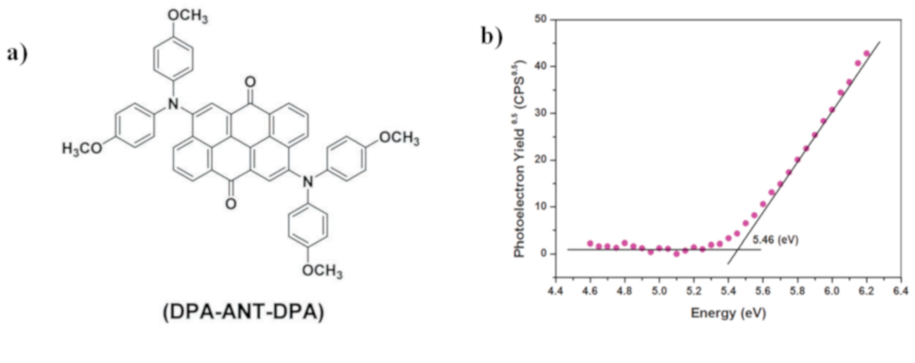
In the search for new HTMs one potential set of candidates involve anthanthrone dye-based systems. The molecule used in this research consists of the anthanthrone dye molecule (ANT) with two functionalized diphenylamine (DPA) end caps. Together the molecule is referred to hereafter as DPA-ANT-DPA. This molecule was synthesized by Pham et al. in 2017 for use as an HTM in perovskite solar cells [
9]. The advantage of this molecule over more familiar chemical interlayers (such as Spiro-OMeTAD
) is that DPA-ANT-DPA is cheaper and it does not require a dopant. The molecule has a donor-acceptor-donor structure and is produced via a one-step synthesis from relatively cheap components. Thus, DPA-ANT-DPA is a simpler and possibly longer lasting interlayer chemical than some other alternatives. This material, once dissolved in an organic solvent, can simply be coated onto a substrate in atmospheric conditions in order to produce a thin, dopant free, hole-transporting layer.
In the perovskite system, interlayer materials of this sort have been shown to provide similar benefits to device performance as Spiro-OMeTAD [
9] with the advantage that the material can be prepared for spin coating in ambient conditions. Similar hole transporting materials have been applied to small area CNT/Si heterojunction devices [
10]. These materials are 4,4′-(naphthalene-2,6-diyl)
bis(
N,
N-
bis(4-methoxyphenyl)aniline) (NAP), and (E)-4′,4‴-etene-1,2-diyl)
bis(
N,
N-
bis(4-methoxyphenyl)-[1″,1‴-biphenyl]-4-amine) (BPV). Both were shown to produce small active area (0.079 cm
2) CNT/Interlayer/Si devices with PCEs higher than 10% thanks to a reduction in recombination at the heterojunction interface.
The work reported in this paper focuses on the application of DPA-ANT-DPA (called DAD hereafter) (see
Figure 1a) for large area CNT/Si solar cells. For large area cells, the challenge of moving the charge carriers over longer distances is of paramount importance to attain the best performance. For the CNT/Si system, methods to enhance the hole transport at the interface are central to ensuring the devices provide the best efficiency. The addition of the DAD as an interlayer between the CNTs and Si was shown to enhance the performance for the large area cells.
2. Materials and Methods
2.1. DAD Preparation
Solid DAD is dissolved at a concentration of 60 mg in 1 mL of chlorobenzene and treated in an ultra-sonic bath for 30 min. The resultant mixture is filtered through a 45-µm pore filter to remove any remaining solid, leaving a deep green suspension.
2.2. CNT Preparation
Bath sonication preparation of suspensions was used in previously published work [
10,
11]. In brief, for the CNTs (Carbon Solutions Inc., Riverside, California), a surfactant solution was formed by adding Triton X-100 to water at a concentration of 1% v/v. This mixture was bath sonicated (≈50 WRMS (root mean squared Watts) (Elmasonic S 30 H)) for 20 min before dry CNTs were added to the mixture at a concentration of 1 mg mL
−1.
2.3. Graphene Oxide (GO) Synthesis
Graphene oxide was used to improve the strength of the SWCNT films. The synthesis method used was based on the paper by Marcano et al. [
12]. In brief, a mixture of graphite flakes and KMnO
4 was prepared and an acidic solution made using a 9:1 ratio of H
2SO
4/H
3PO
4 was added. The mixture was heated to 50 °C and stirred for 12 h. After stirring, the reaction was cooled and poured onto ice made from purified water with 30% H
2O
2. The mixture was sifted to remove any remaining graphite and then centrifuged, with the solid material retained. This material was washed six times, twice with water, twice with 30% HCl, and twice with ethanol. The mixture was centrifuged after each wash. The remaining solid was filtered and vacuum dried overnight at room temperature, leaving dark grey graphene oxide flakes.
2.4. CNT and GO Suspension Preparation
CNTs and GO were mixed at a CNT:GO ratio of 2.25:1 in order to increase the strength of the CNT films. The carbon nanotube/graphene oxide (CNTGO) mixture was bath sonicated in four 20 min periods. The bath water was replaced after each period to keep the bath at around room temperature. Once the suspension was formed, it was centrifuged at 17,500 g for 1 h to remove material that was not well dispersed. The top 2/3 of the centrifuged mixture was collected and the remaining 1/3 was centrifuged for an additional hour to increase yield, with the top 2/3 collected. The centrifuge used was a Beckmann-Coulter Allegra X-22.
2.5. Solar Cell Substrate Preparation
Solar cell substrates were produced from purchased 100 mm thick silicon wafers with a grown 100 nm oxide surface layer which were cleaned in a mixture of 3:1 sulfuric acid and hydrogen peroxide. The wafers were then coated with a thin layer of AZ-1518 positive photoresist before being exposed to UV light through a patterned mask to create a photoresist pattern on the surface. The wafers were then sputter coated with a 5 nm layer of chromium, followed by a 445 nm layer of gold. The photoresist was removed in an acetone bath to produce gold patterned devices via a “lift-off” procedure. The rear contact was prepared by removing the 100 nm oxide layer from the rear of the wafer via etching with buffered oxide etch (BOE; 6:1 NH4F:HF). The exposed silicon was allowed to sit in ambient conditions for 90 min before a 300 nm layer of aluminum was evaporated on to the wafer and was annealed for 30 min at 300 degrees.
The 1.5 cm × 1.5 cm active area of each cell was prepared by etching the 100 nm oxide layer with BOE and then leaving the substrates to sit in air for 30 min.
2.6. DAD Film Deposition
The DAD solution is spin coated onto silicon substrates post BOE etch at various spin speeds for 30 s. A variety of deposition volumes and spin speeds were used to determine and ensure an optimal recipe to produce a good film.
2.7. CNTGO Film Production
CNTGO films were produced from suspension using vacuum filtration. A Buchner flask was attached to a water aspiration vacuum via tubing, and a glass frit was placed in the top with a rubber bung providing the seal. A series of two filter membranes were placed on the frit. The bottom membrane was a mixed cellulose ester (MCE) template membrane (VSWP, Millipore, 0.025 μm pore size). This membrane is patterned with the shape desired for the final film. The second (top) membrane is an MCE membrane (HAWP, Millipore, 0.45 μm pore size). A solution of approximately 250 mL of ultra-pure water containing an aliquot of CNTGO suspension was filtered through this setup. The flow rate of the solution was faster through the patterned hole in the lower membrane than through the 0.05 μm pores. Thus, the nanotubes/graphene oxide was deposited in the same pattern as the lower template paper. After the initial filtration an additional filtration of 250 mL of ultra-pure water was performed in order to ensure any CNTGO residue was washed from the glassware on to the film. Additionally this step could assist in washing some surfactant from the CNTs in the film.
This filtration produced films that could be attached to glass and used for light transmittance and conductivity testing or attached to the silicon substrates for device production.
2.8. CNTGO Film Attachment
Once filtered, the CNTGO films on MCE membrane were attached to the substrates using a floatation method. This method was used to prevent damage to the DAD interlayer during device production. First, the excess MCE around the edges of the CNTGO film was clipped away and the CNTGO film on MCE membrane was placed in an acetone bath for 10 min until the MCE had completely dissolved, leaving a free-floating CNTGO mat in the bath. The acetone (with dissolved MCE) was removed via pipetting until only a very thin layer of acetone remained. The bath was then refilled with acetone for a further 10 min, this was followed by three more acetone refills for 10 min each. After the fifth acetone wash it was replaced with water and the mat was allowed to float for 10 min to flush acetone from the CNTGO matrix. This process was repeated an additional two times to ensure all acetone was removed from the bath. Note that the CNTGO film had a very fluid shape (similar to a jellyfish) when floating in acetone but stabilised and spread into a flat mat when floating in water because of the hydrophobic nature of the CNTs. To attach the free-floating film to a substrate, it was prepared and then submerged underneath the film in the water bath. The substrate was then raised through the solvent, taking the CNTGO film with it. The substrate can be re-submerged to properly align the film until it covers the desired area. The substrate was then carefully dried under a low flow of nitrogen gas stream to avoid dislodging or deforming the film.
2.9. Gold Chloride Doping
Gold chloride (AuCl3) was used to dope the CNTGO film post device fabrication. The doping was performed by dissolving solid chloroauric acid (Sigma-Aldrich) in water at a concentration of 5 mM. The resultant pale-yellow suspension was dropped onto the film and left for 30 s before spin-coating at 5000 rpm for 30 s using a Laurell WS-400B-6NPP/LITE Spin Coater.
2.10. Solar Cell Testing
The performance of the solar cells were tested using a custom LabviewTM virtual instrument connected with a Keithley 2400 source unit. The power density of the collimated Xenon-arc light at the device surface with an AM 1.5G filter was calibrated to be 50 mW cm
−2 by a standard unit cell (PV Measurements, NIST-traceable certification). The power conversion efficiencies (PCE) are reported for the standard 100 mW cm
−2 light intensity. The calibrations undertaken to allow this conversion are provided in the
Supplementary Information.
Following a test of the “as prepared” cells, the SWCNT film was doped using gold chloride and J/V curves were then produced from the doped cells.
2.11. Characterization
SEM images were taken of DAD films formed using different spin rates and/or different deposition volumes. To achieve all SEM images, an Inspect FEI F50 SEM (Hillsboro, OR, USA) was used with beam spot size and high voltage adjusted to optimize the image quality. The image resolution was generally 2048 × 1768 with an imaging speed of 30 μs. The SEM was calibrated using silicon calibration grids (Bruker model numbers PG: 1 μm pitch, 110 nm depth and VGRP: 10 μm pitch, 180 nm depth).
An issue with SEM imaging of thin films is that unless they exhibit a degree of surface roughness, their presence can often be hard to detect as they will appear visually similar to a bare substrate. To overcome this issue, it was decided to manually damage the film either via light scratching with a scalpel or using the laser beam in a Raman microscopy system. The scalpel will remove any polymer layer present on the surface but will have no effect on the much denser silicon underneath. These scratches were useful for AFM imaging to determine film thickness. In the case of the laser-based removal of material, the laser was focussed on the DAD film producing a spectrum with large silicon peaks accompanied by significant noise interference. Over time, the noise reduced to become negligible. At this point, the laser was stopped as it was interpreted that a clean silicon spectrum indicated that essentially all the DAD in the laser area was burnt from the surface. The laser used to remove material was from a Witec alpha300R Raman microscope (Witec, Ulm, Germany) at an excitation wavelength of 532 nm using a ×40 objective with a numerical aperture of 0.60. The power level used was to remove material and was the maximum available on the system which was approximately 30 mW.
Atomic force microscopy (AFM) was performed on solution-processed interlayers on solar device substrates to image the morphology of the films. The thickness of the solution-processed interlayers was measured using AFM by imaging the channels formed in the film with the scalpel, the height of which could be measured from cross sections using the section tool in the analysis software which allows determination of the thickness of the film. Alternatively, thickness could be determined using the depth analysis function in the AFM software and allows an analysis of the height distributions in the images where the level of the substrate and the top of the films could be determined to allow determination of film thickness.
AFM was performed in air using a Bruker multimode 8 AFM with Nanoscope V controller, operating in standard tapping mode. The AFM probes used were silicon HQNSC15/AlBS Mikromasch probes (nominal tip diameter and spring constant is 16 nm and 40 N m−1 respectively). Set-point, scan rate, and gain values were chosen to optimize image quality. The AFM scanner was calibrated in x, y, and z directions using silicon calibration grids (Bruker model numbers PG: 1 μm pitch, 110 nm depth and VGRP: 10 μm pitch, 180 nm depth). AFM topography images have been flattened and thickness measurements taken using Nanoscope Analysis 1.4.
Photoelectron spectroscopy in air (PESA) measurements were conducted using an AC-2 photoelectron spectrometer (Riken-Keiki Co., Tokyo, Japan).
3. Results
SEM images of the DAD films on device substrates were collected. In many cases, the images simply showed a flat topography not unlike that of the bare substrate. As such, to prove the presence of the film, the layer was intentionally damaged and imaged again. In this case, the laser approach to damage the films was used to ablate small holes in the layers. These images are provided in
Figure 2. This clearly demonstrates that the film has been successfully deposited. A fuller set of both optical and SEM images are provided in the
Supplemental Materials in Figures S2 and S3.
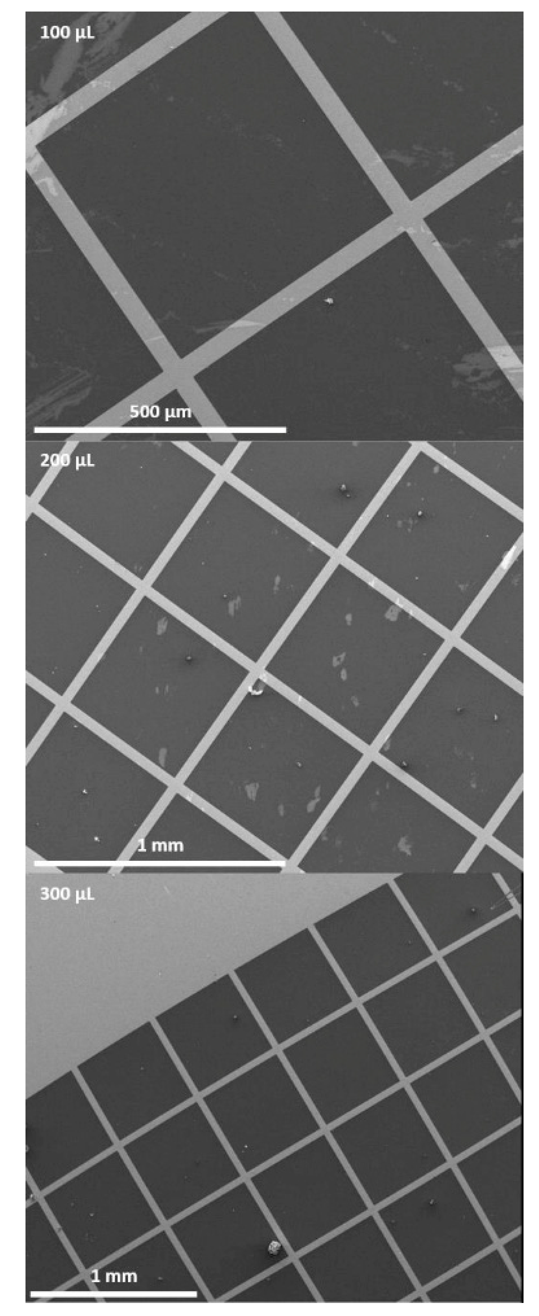
From the SEM images in
Figure 3, it is apparent that the volume of solution spun on the surface has an effect on the film morphology. Lighter coloured regions are visible on the films. They are larger and more frequent in the 100 μL film than in the 200 μL film and there are none visible at all in the 300 μL sample. It is apparent that a volume of at least 300 μL is required to produce a smooth homogenous film. The light-coloured regions are likely thinner areas of film.
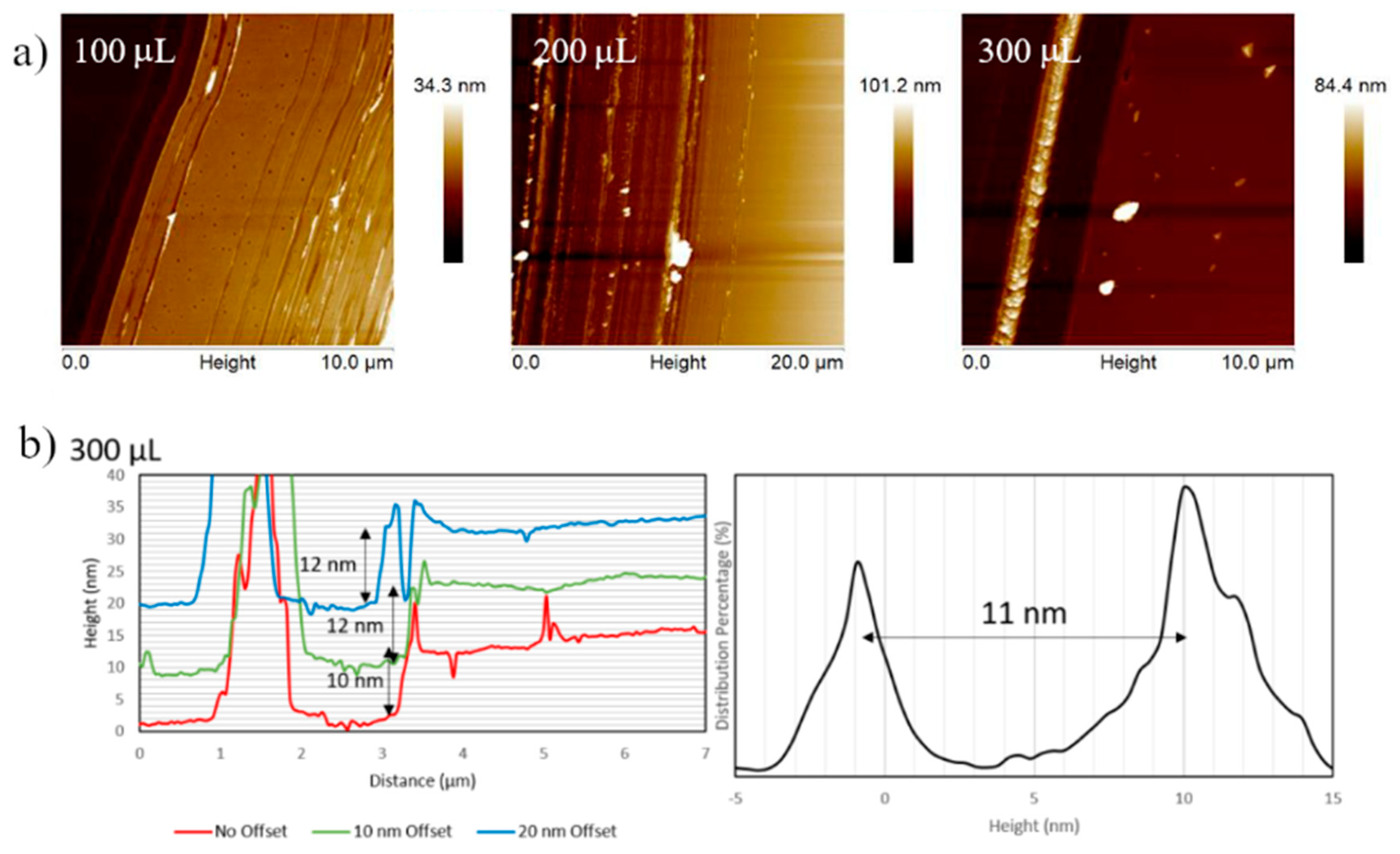
Figure 4 shows the images used to determine the thickness of the DAD layers. A fuller set of data is provided in the
supplementary information for films made with different solution volumes and different spin speeds (
Figures S4–S7). Across the range of volumes used (100 mL to 300 mL) and spin speeds (500 rpm to 7500 rpm), the change in film thickness observed is relatively small. All films appear to have thicknesses in the range of 10–20 nm. Our previous work has shown that this thickness range is ideal as an interlayer. If the layer is thinner, it will typically not be complete which will lower the ability to help with the charge transfer while thicker layers will push the CNTs too far away from the Si and hence the establishment of the heterojunction will be compromised.
From the PESA measurements shown in
Figure 1b, the oxidation potential was measured and the HOMO value of DPA–ANT–DPA was estimated to be −5.46 eV [
9]. The optical properties of the layers made using different spin speeds were measured with uv-vis spectroscopy and the data is provided in
Figure S8. At higher spin speed the films do have less optical density indicating that they are getting thinner. The changes in absorbance from 500 rpm to 7500 rpm are on the order of 40% again suggesting that the thickness of the layers is not changing dramatically which is in line with the observation from the AFM measurements.
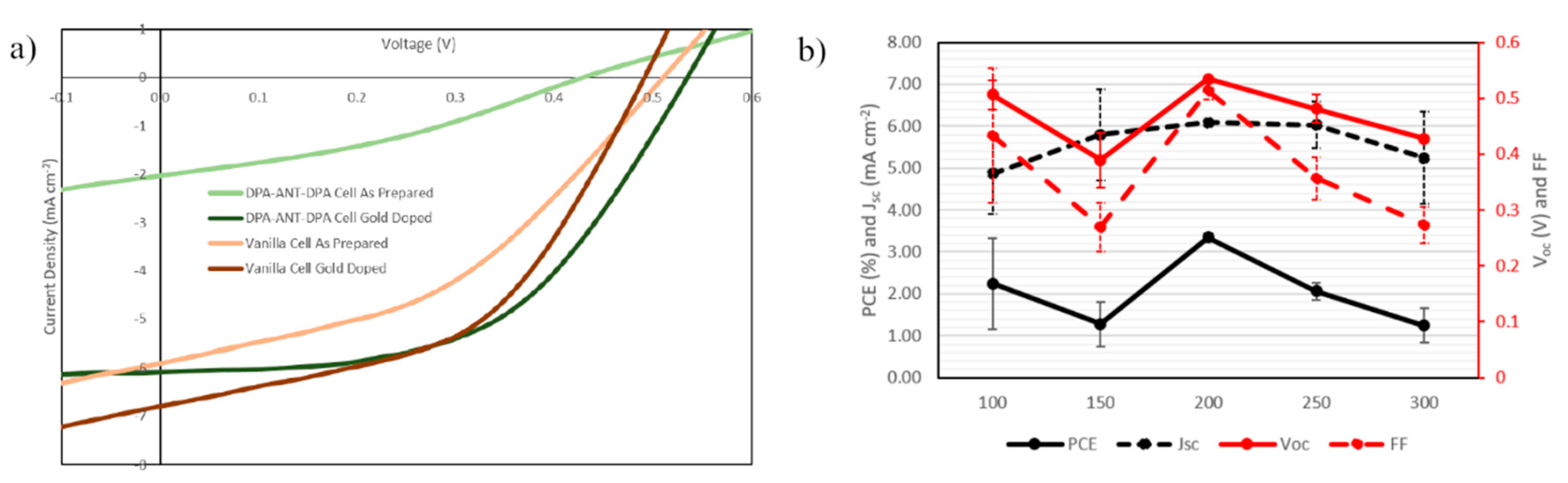
Figure 5 provides representative J/V curves for the control cells and cells with the DAD interlayer while
Table 1 provides a summary of the device performance prepared with various suspension volumes. The addition of DAD has a significant effect on the performance of the devices. The data shows that a volume of 200 μL is optimal to produce the best performing devices as they outperformed the other sets across all parameters. The 150 μL set was the worst performing. However, when the J
sc trend is observed, it is clear that there is still a general trend of improvement with volume up until the 200 μL point. The drop-in performance for the 150 μL devices is due to concurrent drops in V
oc and FF. The J
sc displays the clearest trend, with a peak at 200 μL. Additionally, the 200 μL samples displayed the highest consistency within the device set.
Table 1 shows that the optimal volume of 200 μL outperforms devices with no interlayer by almost 0.50% PCE (14% relative improvement). This is due to an improved V
oc from 0.47 ± 0.02 V to 0.53 ± 0 V and a significantly improved FF from 0.38 ± 0.10 to 0.51 ± 0.02. It is interesting to note that the J
sc is actually lower in the devices with a DAD interlayer than in the devices with no interlayer. However, the difference is less than 1 mA cm
−2 in values in the neighbourhood of 6 mA cm
−2 and thus it can be seen that the enhancements in V
oc and FF outweigh the decrease in J
sc.
The J/V curves for the best performing device with DAD and without are shown in
Figure 4a. These curves show the difference in effect of the AuCl
3 dopant on the devices. For the device with no interlayer, the AuCl
3 improved the Jsc from 5.90 to 6.79 mA cm
−2 (a 15.1% improvement), improved the FF from 0.42 to 0.49 and lowered the V
oc from 0.51 to 0.49 V. Overall this produced a PCE gain from 2.52 to 3.24% (a 28.6% improvement). The changes exhibited in the device with a DAD interlayer were far more pronounced. The J
sc improved from 2.03 to 6.08 mA cm
2 (a 200% improvement) while the FF increased from 0.34 to 0.53 and the V
oc increased from 0.43 to 0.53 V. Giving an overall PCE improvement of 0.59 to 3.44% (a 483% improvement). After AuCl
3 doping, the parameters for the device with the DAD interlayer are superior to the device with no interlayer, with the exception of the J
sc. This matches the comparison seen between the average values (
Table 1). Additionally, the deviation in PCE values was much smaller for the devices with the DAD interlayer than in those without, ± 0.10% vs. ± 0.66%. This clearly indicates that the addition of a DAD HTM improves the performance of the large area CNT/Si heterojunction solar device.
The improvement because of the AuCl
3 treatment is largely due to an improvement in conductivity of the CNTs layer after the doping. The sheet resistance of CNTGO films before doping was 580 ± 5 Ω/sq and 199 ± 7 Ω/sq after doping. The improvement in conductivity is well established and due to the deposition of Au nanoparticles on the CNTs although the anions in the solution are thought to play a role as well [
13,
14]. Similar effects with Pt spheres have been observed [
15]. This effect should be very similar with and without the DAD present. However, there does seem to be an extra enhancement with the interlayer present. This could be due to a modification of the DAD layer upon exposure to the AuCl
3. Uv-vis spectroscopy shown in
Figure S9 shows that there is very little change in the optical properties of the layer, and it is unlikely that the improvements are due to higher transmittances of the interlayer leading to more light reaching the silicon. The mostly likely reason for the extra improvement in performance is that the presence of the liquid for a short period makes the CNT/DAD interface somewhat “fluid” and components in the two layers can shift slightly leading to better contacts at the interface.
The smoothest and most homogenous film (
Figure 3, 300 μL) is not the one that gives the best device performance. The existence of the lighter coloured regions appears to be required to improve device performance as the homogeneous films formed with a 300 μL suspension did not produce the best performing devices. The reason for this could be that the thinner regions allow a better CNT/Si junction to be formed. Thus, the peak in PCE for different DAD volumes is a trade-off between having enough thin areas in the DAD film to allow CNT/Si junction formation whilst the film being homogeneous enough to improve charge carrier extraction.
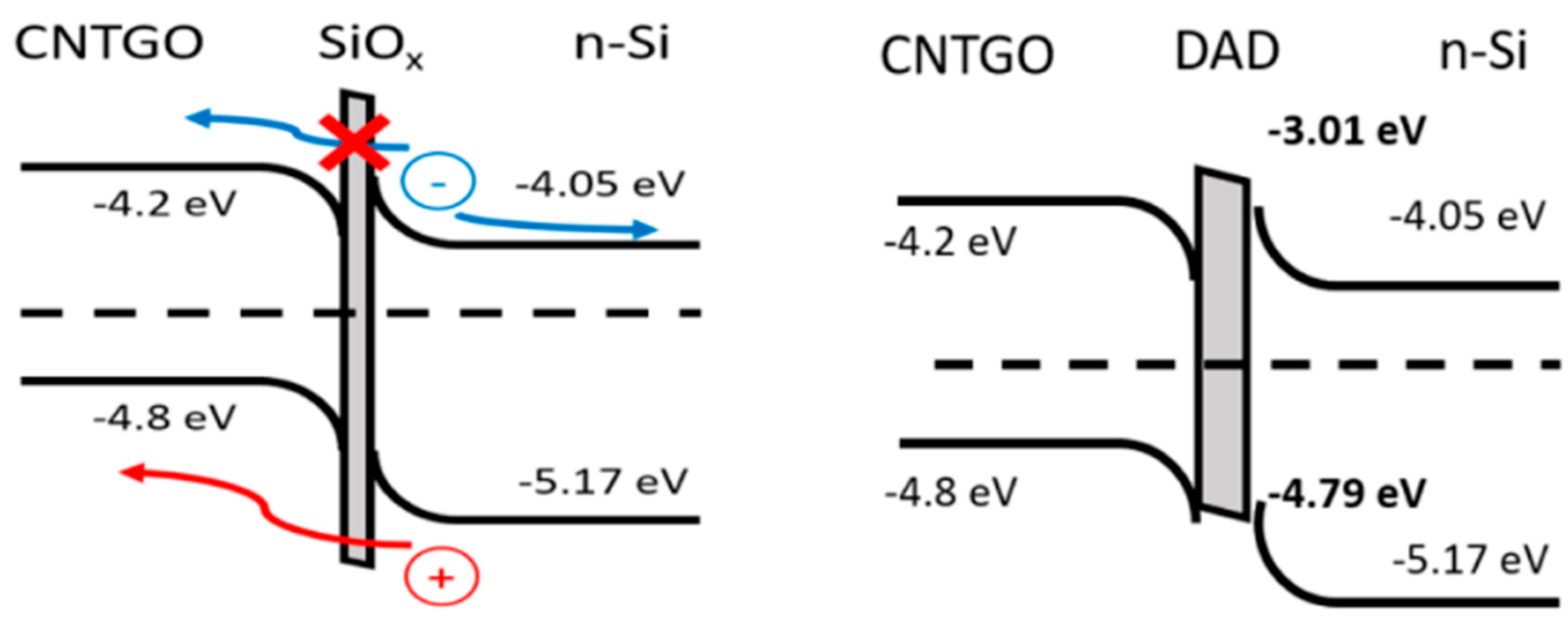
The improvement in performance for the cells after the addition of a DAD interlayer is due to two main reasons. The first is that the DAD layer will form a conformal covering on the silicon surface, whereas sparse CNT networks limit the overall photoactive junction interfacial area because of a smaller area with intimate contact between the p-type and n-type material. Addition of the CNTs onto a softer DAD layer will allow the CNTs to imbed in the layer proving better contact thus making charge transport more efficient. This encapsulation of the CNTs by the DAD layer is enhanced in the doping step which sees further device performance improvements. The second important consideration is the energy levels shown in
Figure 6 [
9]. The DFT-calculated energy levels differ slightly from the experimental values because of the gaseous state assumptions. CNTs are ambipolar and hence can conduct both holes and electrons. This means the CNTs are potential sites for recombination of charge carriers which will significantly lower the efficacy of the solar cells. Thus, any steps to limit the transport of one type of charge carrier into the CNT layer can improve the device performance. It is clear from past studies that a thin oxide layer is ideal for optimizing photovoltaic performance in CNT/Si devices [
16]. The DAD layer limits the movement of electrons into the CNTs while improving hole transport and is much easier to control than oxide growth so it represents an important development in maximizing the efficiencies of the CNT/Si solar cells.


 ,
, 


