Article

Design and Application Research of All-Dielectric Nanostructure Colorful Display

College of Liberal Arts and Sciences, National University of Defense Technology, Changsha 410073, China
*
Author to whom correspondence should be addressed.
Appl. Sci. 2019, 9(14), 2937; https://doi.org/10.3390/app9142937
Submission received: 19 June 2019 / Revised: 12 July 2019 / Accepted: 17 July 2019 / Published: 23 July 2019
(This article belongs to the Special Issue Advanced Active and Passive Metasurfaces)

Abstract

:
Structural colors generated by plasmonic resonances in metallic nanostructures have been intensively studied and exciting progress has been made. However, because of the inherent plasmon damping, the saturation of these colors generated by metallic nanostructures could not meet the needs of industrial applications. As a result, researchers increasingly focus on structural colors generated by all-dielectric nanostructures. In this paper, we discuss a type of all-dielectric nanostructure based on a previous design and analyze its optical properties extensively. The display of character T with different color is realized by using this nanostructure. The study helps the understanding of the influence of structural parameters on structural color and provides some guidance for future experiments. This work can impact the development of the structural color devices which can be applied in color printing, color displays, color filters, imaging, and energy harvesting, etc.

1. Introduction

Over the past decade, there has been an on-going wave of interest and effort in developing optical metamaterials which exhibit exotic electromagnetic properties [1,2,3]. These metamaterials, constructed with subwavelength building blocks that are artificially arranged in 3D configurations, can be used to obtain novel optical phenomena that are unattainable from materials which exist in nature. Plasmonic colors, which emerge from resonant interactions between light and metallic nanostructures, are examples of such novel optical phenomena and can be used in color printing, filters, etc. [4]. Plasmonic resonances of metallic nanostructures have enabled high-resolution color printing beyond the optical diffraction limit at a resolution of ~100,000 dots per inch [5,6,7,8]. Plasmonic metasurfaces are easy to fabricate and have the ability of unprecedent control over the reflected or transmitted light while featuring relatively low losses even at optical wavelengths [9]. More importantly, today’s optical techniques demand the compaction of the physical dimensions of optical systems and development of a smaller and low-energy system [10]. Hence, plasmonic metasurfaces, which can be considered as the two-dimensional analog of metal-based metamaterials, have attracted increasing attention over recent years [9]. However, metallic nanostructures have inherent plasmon damping and possess mainly electric-like resonances. Plasmonic colors suffer from poor color saturation with a gamut that occupies only a small subset of perceivable colors on the International Commission on Illumination (CIE) 1931 chromaticity diagram [5]. Thus, there is an urgent need for another degree of controlling of structural colors, for example, the magnetic resonance modes [11]. The all-dielectric nanostructures which generate structural colors of high saturation and high resolution then entered the view of researchers [12,13,14,15,16,17]. Furthermore, finding materials that achieve broadband absorption and are eco-friendly is also a long-sought-after goal of researchers [18,19]. Based on previous research [5], this paper uses silicon nanostructures, which are fabricated onto a silicon substrate divided with a Si3N4 layer, to realize the display of different colors. Instead of metals, silicon nanostructures exhibit localized magnetic and electric dipole resonances and can achieve relatively high transmission efficiency with full phase range control, low costs and wide application prospects. It is well known that slight changes in the parameters of nanostructures will create major shifts in perceived colors [20]. Therefore, we further analyze the impact of nanostructure parameters, and find that the diameter of nanodisk decides the distribution of structural colors. The height of the nanodisk and thicknesses of the dielectric layer and substrate mainly have effects on the saturation of structural color. Finally, we use the nanostructures to realize the display of letter T with three different colors.

2. Design of Unit Cell Structure

The designed unit cell of the all-dielectric nanostructure consists of a silicon nanodisk and a silicon substrate separated by a Si3N4 dielectric layer, as shown in Figure 1. D denotes the diameter of the nanodisk with height h. Hd is the height of the Si3N4 dielectric layer, and Hs is the height of the silicon substrate. p denotes the period of the unit cell. The central axis of the nanodisk coincides exactly with the central axis of the dielectric layer.
We use the finite-difference time-domain (FDTD) solutions software to analyze the reflection characteristics of the nanostructure illuminated by a vertical incident light, whose electric field is polarized along the x direction, and set the working wavelength range as 400–700 nm. The boundary conditions in x and y directions are periodic, whereas the boundary conditions in the z directions are perfect matching layers (PML). According to previous studies [5], we chose h = 130 nm and Hd = 70 nm. We found the optimal height of the substrate Hs to be about 140 nm by running Parameter Sweep and observing the reflection spectra at different Hs, which was also verified by the distance between the chromaticity coordinate of reflection spectra and that of the standard color.
Simulation results are shown in Figure 2. When D is 190 nm and both of the period p in the x and y directions are 290 nm, the maximal reflection peak of the spectra is lying in the red band, as shown in Figure 2a. When D is 115 nm and the period p is 290 nm, the reflection spectra with maximal peak in green band can be obtained, as shown in Figure 2b. When D is 100 nm and the period p is 190 nm, the maximal reflection peak of spectra is in the blue band, as shown in Figure 2c.
To understand the resonant modes inside the nanostructures, we take the structure with D = 190 nm and p = 290 nm as an example. The corresponding electric dipole (ED) and magnetic dipole (MD) resonances are shown in Figure 2d,e, respectively. It can be seen clearly from Figure 2 that magnetic resonance and electric resonance coexist, but the electric resonance shows higher intensity. The electric dipole and magnetic dipole resonances play an important role in increasing the absorption of light and enhancing the transmission efficiencies [21,22,23].
Using above nanostructures, we can obtain a variety of reflection spectra corresponding to different colors by changing the diameter D or the period p of nanostructures. Assuming the obtained reflection spectra are R ( λ ) , the X, Y, Z components can be obtained from the following formulae:
{ X = 400 700 R ( λ ) x d λ Y = 400 700 R ( λ ) y d λ Z = 400 700 R ( λ ) z d λ ,
where x , y , z are the matching functions. Then, we can obtain the chromaticity coordinates (x, y) by x = X / ( X + Y + Z ) and y = Y / ( X + Y + Z ) . The corresponding chromaticity coordinates in the International Commission on Illumination’s (CIE) 1931 chromaticity diagram based on the measured reflectance spectra from simulations are shown in Figure 2f. On the one hand, the resonances are not equally excited under the different parameters of the nanostructure. On the other hand, the absorption of silicon to blue light is more intense from the trend of the permittivity of silicon with wavelength. Hence, we can find that the blue is weaker than red and green from the chromaticity diagram. Even so, we think that rich colors can be obtained by improving the parameters of nanostructures, and this can be potentially used for colorful display.

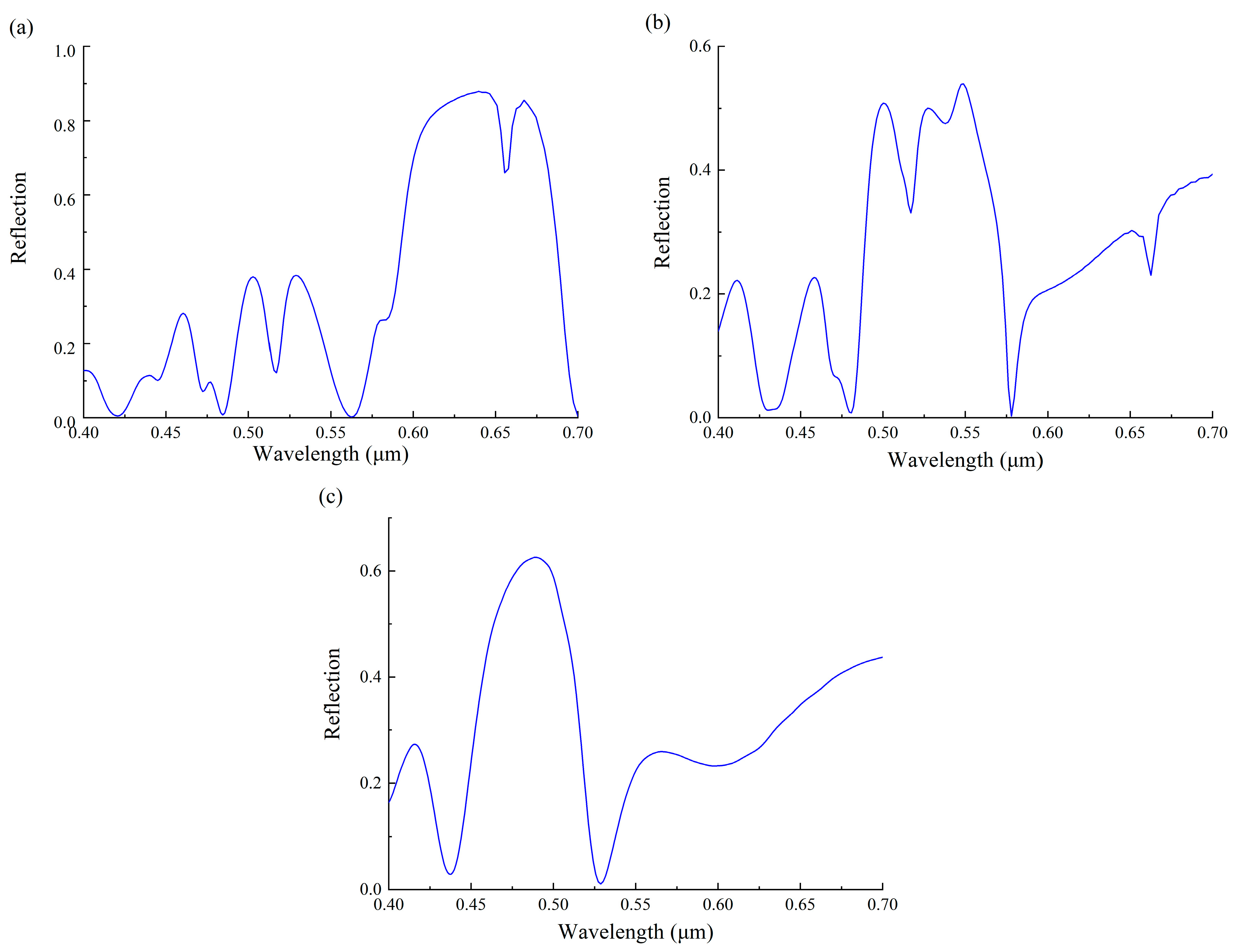
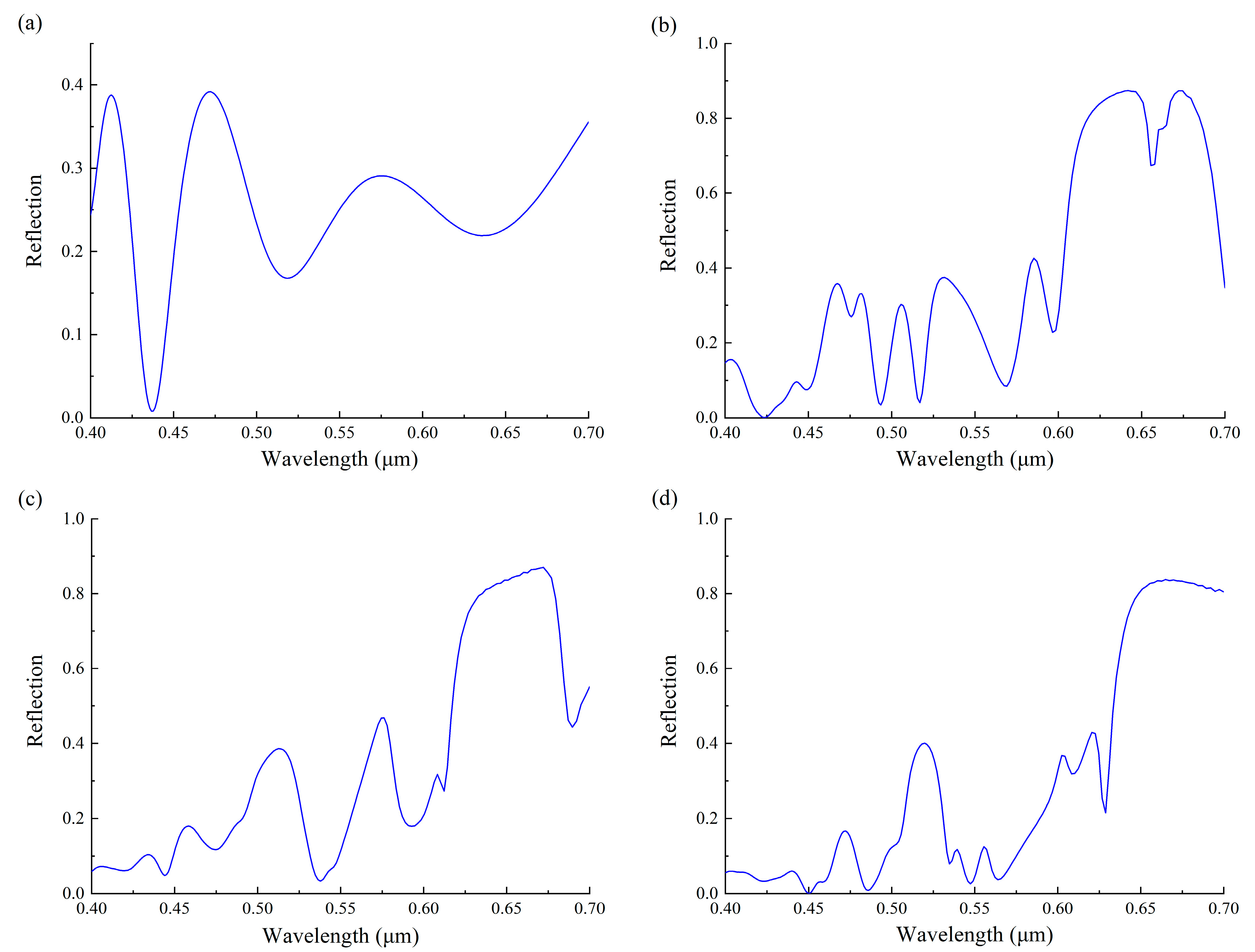
3. The Influence of Structure Parameters

It is well known that slight changes of nanostructures’ parameters will largely shift the structural color. How much the parameters of nanostructures influence the structural color is the topic to be discussed in this section. To systematically analyze the influences of the nanostructure parameters on structural colors, such as the diameter of nanodisk, the height of nanodisk, the tilt angle, the thickness of dielectric layer, and the thickness of substrate, we chose a set of parameters in which the nanostructure reflected the red wave band to perform numerical simulations using the finite-difference time-domain method. According to the simulation results in Section 2, these parameters include 190 nm for D, 290 nm for the period p, and 130 nm, 70 nm, 140 nm for h, Hd, Hs, respectively.

3.1. The Diameter of Nanodisk

From previous studies [5], we know that the diameter of nanodisk is the main factor affecting the structural color. The influence of the gap size between nanodisks on the structural color is less important because light can be tightly confined in the nanodisk due to its high refractive index. The influence of the diameter of nanodisk on the distribution of the reflectance spectra is discussed in the following section. Keeping the center-to-center distance of the nanodisks unchanged, that is, p is kept fixed, we observe the variation of reflectance spectra by changing the diameter of the nanodisk D from 30 nm to 200 nm. The results show that the center wavelength of the maximal reflection peak lies in the blue band when the diameter is minimum, as shown in Figure 3a. As the diameter D increases, the maximal reflection peak of the spectra gradually shifts to longer wavelengths and reaches about 642 nm with full width at half-maximum (FWHM) around 95 nm when D = 200 nm, as shown in Figure 3b. In the above simulation, the period p is invariable, so the gap size between nanodisks g gradually decreases as the diameter of nanodisk D increases, where g = pD. In order to verify whether the diameter of nanodisk D is also a main factor affecting structural color when gap size between nanodisks g remains unchanged, we performed the simulation again. The difference is that the period p changes as D varies, but g is invariable. The results show the same variation trend compared with simulations of p unchanged, except that the spectral distribution is slightly different, as shown in Figure 3c,d. The above simulation results confirm that the diameter of the nanodisk has a decisive effect on the structural color, compared with the gap size between nanodisks.

3.2. The Height of Nanodisk

To study the impact of the height of nanodisk on the structural color, we gradually changed the height of nanodisk h from 30 nm to 220 nm with all other parameters kept at fixed values, and simulated again with Parameter Sweep function in FDTD. Simulation results show that the variation of the height of nanodisk has a large impact on the structural colors. When h is small, the reflection spectra have many separated peaks, as shown in Figure 4a. Namely, the reflected light is a less saturated red. As h increases, some peaks gradually decrease and finally vanish, while others grow higher and wider, as shown in Figure 4b. When the height of nanodisk h increases to 130 nm, the bandwidth of the red peak reaches the maximum, and the saturation of the reflected light is closest to the standard red. Following this, as the value of h continues to increase, the color saturation of the reflected light begins to decrease. This can be concluded by the distances from every chromaticity coordinate of different spectra to that of standard red. The chromaticity coordinates corresponding to different h have been marked in the chromaticity diagram, as shown in Figure 4c.

3.3. The Tilt Angle

In this section, we discuss the impact of the tilt angle of incident plane wave on structural color. All parameters of the nanostructure unit cell are kept at fixed values, while the tilt angle of incident plane wave is changed from −30° to 30°. We use FDTD solutions to simulate again. According to the simulation results shown in Figure 5a–d, we find that changing the tilt angle of the incident light hardly affect the distribution of the spectra, but the value of each reflection peak, that is, the reflectivity, gradually decreases as the tilt angle increases. In order to verify the polarization insensitivity of the nanostructure, we rotated the electric field direction by 90° and ran the simulation again. Parts of the results are shown in Figure 5e,f. These simulation results indicate that the change of tilt angle of incident plane wave will not influence the structural color but affect the visual effect of structures in brightness.

3.4. The Thickness of Dielectric Layer

The thickness of the dielectric layer Hd is another factor which could affect the structural color. Therefore, we changed the thickness of the dielectric layer Hd from 30 nm to 120 nm while keeping other parameters unchanged, and ran the simulation again. Results show that when the thickness of the dielectric layer is less than 70 nm, the reflectivity and the bandwidth of the red wave band increase as the thickness of the dielectric layer increases, but the reflectivity of the blue and green wave bands decreases. When the dielectric layer is thicker than 70 nm, the reflectivity and the bandwidth of the red wave band increase, and so does the reflectivity of the green and blue wave bands. Therefore, we can draw the conclusion that when the thickness of the dielectric layer Hd is 70 nm, the reflected light is the closest to the spectral red, which is the result we want, as shown in Figure 6.

3.5. The Thickness of Substrate

To investigate the influence of the thickness of substrate on reflected light, we kept all other parameters fixed and change only the thickness of the substrate Hs from 100 nm to 300 nm and ran the simulation again. Results show that the changes of the reflection spectra are complex. A monotonous increase or reduction with the increase of the thickness of substrate does not exist.
With the thickness of the substrate Hs increasing, it is clear that the peak position tends to shift towards shorter wavelength, and the maximal peak always lies in the red band, but the bandwidth of the maximal peak varies periodically, as shown in Figure 7. This is because the position of the maximal reflectivity is decided by the structural size of the nanodisk, and the thin-film interference gives the reflectivity more detail. The incident light reaching the dielectric layer, experiences multilayer interference at the air-dielectric interface because of the existence of the dielectric layer and the substrate. According to the thin-film interference theory, when the wavelength of light under normal incidence meets the formula
2 H d n 1 + 2 H s n 2 = ( m 1 2 ) λ ,
Where n1 and n2 are the refractive index of dielectric layer and substrate respectively, constructive interference will occur. As a result, the reflectivity of the corresponding positions will increase, which will lead to the increase of the saturation of the reflected light expected to be red. For example, when Hs = 100 nm, 170 nm and 270 nm, the saturation of the reflected light gets lower, as shown in Figure 7a,c,e. On the other hand, due to the existence of the multilayer interference, the spectra change periodically. For instance, the spectra at Hs = 140 nm and Hs = 230 nm are similar. When Hs = 140 nm, the maximum reflectivity is about 87.8% and the FWHM is about 95 nm. When Hs=230 nm, the maximum reflectivity is about 88% and the FWHM is about 90 nm, as shown in Figure 7b,d.
From the above simulations, we find that the diameter of nanodisk has a great influence on the distribution of the structural color, that is, the diameter of the nanodisk decides the hue of structural color, while the height of the nanodisk, the thicknesses of the dielectric layer and substrate mainly have effects on the saturation of structural color. The tilt angle has no impact on the hue and the saturation of the structural color but influence its brightness. According to this conclusion, we can obtain the colormap based on FDTD simulations by adjusting the diameter of the nanodisk from 30 nm to 210 nm and gap size g from 20 nm to 200 nm, as shown in Figure 8.

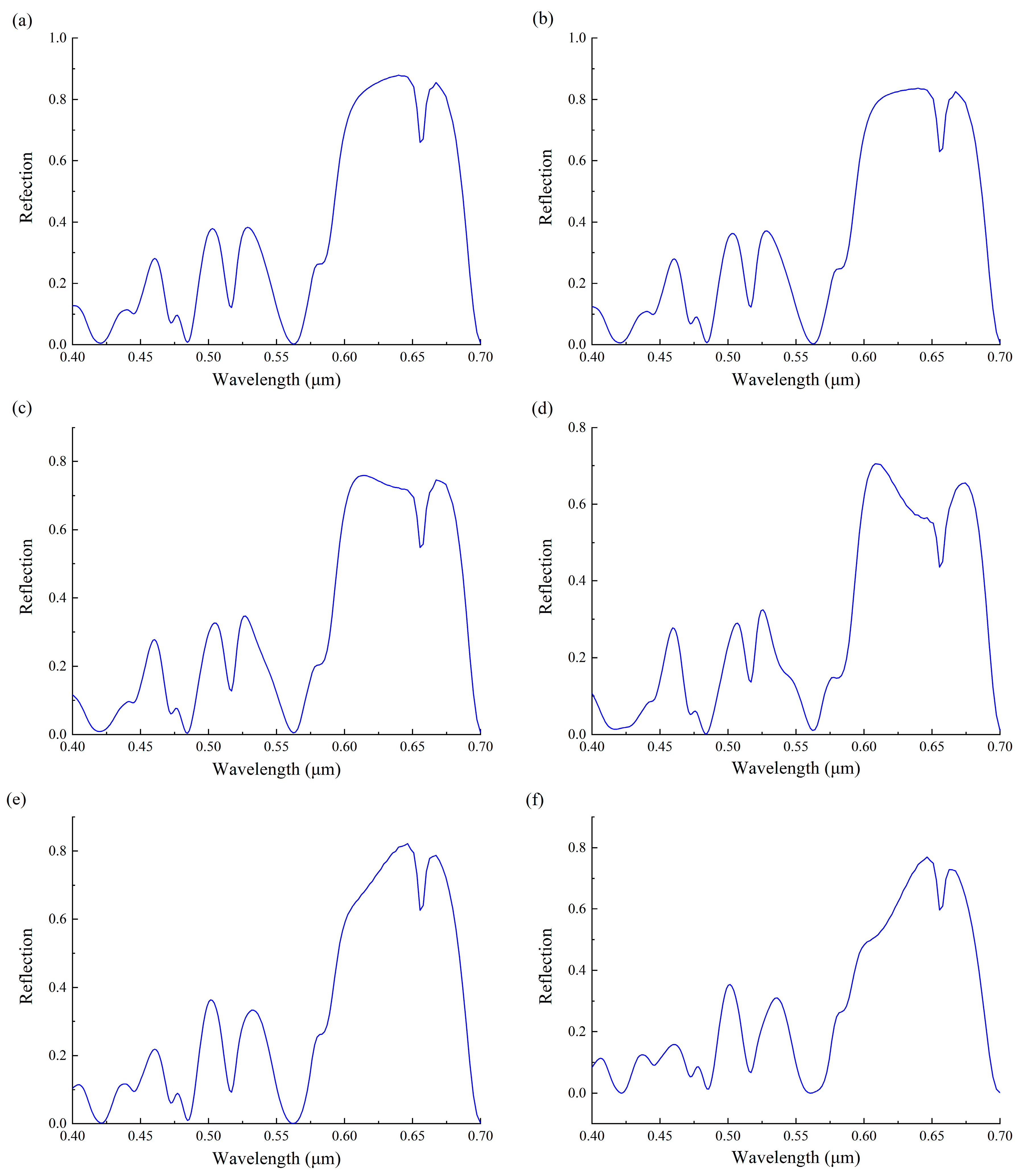
4. Application for Color Display

In this section, we used silicon nanodisks to realize the display of the letter T in different colors. From the results in Section 3, we know that the diameter of the nanodisk has a great influence on the hue of the structural color, while the height of the nanodisk, the thicknesses of dielectric layer and substrate mainly affect the saturation of the structural color. Therefore, the letter T with different colors can be obtained by only changing the diameter of nanodisk D and keeping the height of nanodisk and the thicknesses of the dielectric layer and the substrate at their optimal values (130 nm, 70 nm and 140 nm, respectively). Here, the letter T consisted of 6300 nanostructure unit cells and every nanostructure unit cell is the same as the one shown in Figure 1. The horizontal part of the letter T was made up of 50 rows × 75 columns of nanodisks, and the vertical part of the letter T consisted of 50 rows × 51 columns of nanodisks. We set the diameter of every nanodisk at 190 nm, the gap size between nanodisks to be 100 nm, and obtained a red letter T. A part of the corresponding red reflection spectra is shown in Figure 9a. By adjusting the diameter of the nanodisk to 115 nm and the gap size between nanodisks to 175 nm, we obtained a green letter T. A part of the green reflection spectra is shown in Figure 9b. By adjusting the diameter of the nanodisk to 100 nm and the gap size between nanodisks to 90 nm, the blue letter T was obtained. A part of the blue reflection spectra is shown in Figure 9c. In the above simulations, the boundary conditions in x and y directions are periodic, and in the z directions are PML.
As the amount of the simulation calculation is too large to be performed by our workstation, the incident wavelength was divided into several segments. Taking the red letter T as an example, the wavelength of the incident light is between 600–680 nm in Figure 9a, and the reflectivity is greater than the other wavelength according to the simulation. Due to using the same parameters, the letter T has the same reflection spectra as the individual nanostructure, and the color of the letter T would be the same as that of the individual nanostructure. From the reflection spectra simulated in Section 2, we can obtain the color of individual nanostructure by calculating the chromaticity coordinate. After, we can get the dyeing diagram of different color letter T by recoloring the electric field distribution diagram obtained from the monitor in FDTD Solutions, as shown in Figure 10.
Based on the above results, we know that these letter Ts composed with different nanostructures have a good reflection on the corresponding wave band. In other words, the simulated color of the letter T with different structural parameters is consistent with what we expected.

5. Conclusions

In summary, we discuss a type of all-dielectric nanostructure based on previous research [5] and analyzed its optical properties by changing the diameter of the nanodisk, the height of the nanodisk, the tilt angle, and the thicknesses of the dielectric layer and substrate. We found that the diameter of nanodisk has a great influence on the distribution of the structural color, while the height of the nanodisk and the thicknesses of dielectric layer and substrate mainly affect the saturation of the structural color. The tilt angle has no impact on the hue of the structural color but influences its brightness. Afterwards, we used these nanostructures to realize the display of different colors of the character T based on our parameter analysis. The simulation results are consistent with theoretical predictions. This study helps the understanding of the influence of structural parameters on structural color and could provide guidance for future experiments.

Author Contributions

J.Y. proposed the frame of the manuscript and provided specific guidance during the whole research process. S.L. performed all the simulations, data curation and analysis, wrote the original draft and revised the manuscript. X.H. provided theory guidance during the simulation process. S.Z. provided help in the data processing and revised the manuscript. Y.C. revised the manuscript.

Funding

This work is supported by the National Natural Science Foundation of China (61671455, 61805278), the Foundation of NUDT (ZK17-03-01), the Program for New Century Excellent Talents in University (NCET-12-0142), and the China Postdoctoral Science Foundation (2018M633704).

Conflicts of Interest

The authors declare no conflict of interest.

References

  1. Su, V.C.; Chu, C.H.; Sun, G.; Tsai, D.P. Advances in optical metasurfaces-fabrication and applications. Opt. Express 2018, 26, 13148–13182. [Google Scholar] [CrossRef] [PubMed]
  2. Kuester, E.F.; Mohamed, M.A.; Piket-May, M.; Holloway, C.L. Averaged transition conditions for electromagnetic fields at a metafilm. IEEE Trans. Antenn. Propag. 2003, 51, 2641–2651. [Google Scholar] [CrossRef]
  3. Bomzon, Z.; Biener, G.; Kleiner, V.; Hasman, E. Space-variant Pancharatnam-Berry phase optical elements with computer-generated subwavelength gratings. Opt. Lett. 2002, 27, 1141–1143. [Google Scholar] [CrossRef] [PubMed]
  4. Kristensen, A.; Yang, J.K.W.; Bozhevolnyi, S.I.; Link, S.; Nordlander, P.; Halas, N.J.; Mortensen, N.A. Plasmonic colour generation. Nat. Rev. Mater. 2016, 2, 14. [Google Scholar] [CrossRef]
  5. Dong, Z.G.; Ho, J.F.; Yu, Y.F.; Fu, Y.H.; Paniagua-Dominguez, R.; Wang, S.; Kuznetsov, A.I.; Yang, J.K.W. Printing Beyond sRGB Color Gamut by Mimicking Silicon Nanostructures in Free-Space. Nano Lett. 2017, 17, 7620–7628. [Google Scholar] [CrossRef] [PubMed]
  6. Duan, X.Y.; Kamin, S.; Liu, N. Dynamic plasmonic colour display. Nat. Commun. 2017, 8, 14606. [Google Scholar] [CrossRef] [Green Version]
  7. Tan, S.J.; Zhang, L.; Zhu, D.; Goh, X.M.; Wang, Y.M.; Kumar, K.; Qiu, C.W.; Yang, J.K.W. Plasmonic Color Palettes for Photorealistic Printing with Aluminum Nanostructures. Nano Lett. 2014, 14, 4023–4029. [Google Scholar] [CrossRef] [PubMed]
  8. Karthik, K.; Duan, H.G.; Hegde, R.S.; Koh, S.C.W.; Wei, J.N.; Yang, J.K.W. Printing colour at the optical diffraction limit. Nat. Nanotechnol. 2012, 7, 557–561. [Google Scholar]
  9. Ding, F.; Yang, Y.Q.; Deshpande, R.A.; Bozhevolnyi, S.I. A review of gap-surface plasmon metasurfaces fundamentals and applications. Nanophotonics 2018, 7, 1129–1156. [Google Scholar] [CrossRef]
  10. Chen, B.H.; Wu, P.C.; Su, V.C.; Lai, Y.C.; Chu, C.H.; Lee, I.C.; Chen, J.W.; Chen, Y.H.; Lan, Y.C.; Kuan, C.H.; et al. GaN Metalens for Pixel-Level Full-Color Routing at Visible Light. Nano Lett. 2017, 17, 6345–6352. [Google Scholar] [CrossRef]
  11. Zhu, T.; Liu, Y.; Liu, C.; Li, J.; Wang, Y.; Yu, Z.Y.; Yu, L.; Ye, H. All-dielectric colored truncated cone metasurfaces with silicon mie magnetic resonators. Proc. SPIE 2019, 10942, 109420R. [Google Scholar]
  12. Paniagua-Domínguez, R.; Yu, Y.F.; Miroshnichenko, A.E.; Krivitsky, L.A.; Fu, Y.H.; Valuckas, V.; Gonzaga, L.; Toh, Y.T.; Kay, A.Y.S.; Luk’yanchuk, B.; et al. Generalized Brewster effect in dielectric metasurfaces. Nat. Commun. 2016, 7, 10362. [Google Scholar] [CrossRef] [PubMed]
  13. Nicolas, B. Silicon photonics: Large-scale dielectric metasurfaces. Nat. Mater. 2015, 14, 664–665. [Google Scholar]
  14. Park, H.; Dan, Y.; Seo, K.; Yu, Y.J.; Duane, P.K.; Wober, M.; Crozier, K.B. Filter-Free Image Sensor Pixels Comprising Silicon Nanowires with Selective Color Absorption. Nano Lett. 2014, 14, 1804–1809. [Google Scholar] [CrossRef] [PubMed]
  15. Liu, X.Y.; Fan, K.B.; Shadrivov, I.V.; Padilla, W.J. Experimental realization of a terahertz all-dielectric metasurface absorber. Opt. Express 2017, 25, 191–201. [Google Scholar] [CrossRef] [PubMed]
  16. Jahani, S.; Jacob, Z. All-dielectric metamaterials. Nat. Nanotechnol. 2016, 11, 23–36. [Google Scholar] [CrossRef] [PubMed]
  17. Park, C.S.; Koirala, I.; Gao, S.; Shrestha, V.R.; Lee, S.S.; Choi, D.Y. Structural color filters based on an all-dielectric metasurface exploiting silicon-rich silicon nitride nanodisks. Opt. Express 2019, 27, 667–679. [Google Scholar] [CrossRef] [PubMed]
  18. Molet, P.; Garcia-Pomar, J.L.; Matricardi, C.; Garriga, M.; Alonso, M.I.; Mihi, A. Ultrathin Semiconductor Superabsorbers from the Visible to the Near-Infrared. Adv. Mater. 2018, 30, 1705876. [Google Scholar] [CrossRef] [PubMed]
  19. Espinha, A.; Dore, C.; Matricardi, C.; Alonso, M.I.; Goñi, A.R.; Mihi, A. Hydroxypropyl cellulose photonic architectures by soft nanoimprinting lithography. Nat. Photon. 2018, 12, 343–348. [Google Scholar] [CrossRef]
  20. Henrie, J.; Kellis, S.; Schultz, S.M.; Hawkins, A. Electronic Color Charts for Dielectric Films on Silicon. Opt. Express 2004, 12, 1464–1469. [Google Scholar] [CrossRef]
  21. Decker, M.; Staude, I.; Falkner, M.; Dominguez, J.; Neshev, D.N.; Brener, I.; Pertsch, T.; Yuri, S.K. High-efficiency dielectric Huygens’ surfaces. Adv. Opt. Mater. 2015, 3, 813–820. [Google Scholar] [CrossRef]
  22. Liu, S.; Vaskin, A.; Campione, S.; Wolf, O.; Michael, B.; Reno, S.J.; Gordon, A. Keeler Isabelle Staude, Igal Brener. Huygens’ metasurfaces enabled by magnetic dipole resonance tuning in split dielectric nanoresonators. Nano. Lett. 2017, 17, 4297–4303. [Google Scholar] [CrossRef] [PubMed]
  23. Rocco, D.; Carletti, L.; Locatelli, A.; De Angelis, C. Controlling the directivity of all-dielectric nanoantennas excited by integrated quantum emitters. JOSA B 2017, 34, 1918–1922. [Google Scholar] [CrossRef]
Figure 1. Schematic diagram of the nanostructrue unit cell.
Applsci 09 02937 g001
Figure 2. The reflection spectra and the field distribution. (a) The reflection spectra with D = 190 nm and p = 290 nm. (b) The reflection spectra with D = 115 nm and p = 290 nm. (c) The reflection spectra with D = 100 nm and p = 190 nm. (d) The electric dipole resonances with D = 190 nm, p = 290 nm and λ = 600 nm. (e) The magnetic dipole resonances with D = 190 nm, p = 290 nm and λ = 680 nm. (f) The CIE 1931chromaticity diagram obtained from the reflection spectra with different D and p. D varies from 30 nm to 200 nm. p takes the value of 140 nm, 190 nm and 290 nm, respectively.
Applsci 09 02937 g002aApplsci 09 02937 g002b
Figure 3. The reflection spectra of different D. (a) The reflection spectra with D = 30 nm when p is invariable. (b) The reflection spectra with D = 200 nm when p is invariable. (c) The reflection spectra with D = 180 nm when p is variable. (d) The reflection spectra with D = 200 nm when p is variable.
Applsci 09 02937 g003
Figure 4. The reflection spectra of different h and the corresponding chromaticity diagram. (a) The reflection spectra with h = 40 nm. (b) The reflection spectra with h = 80 nm. (c) The chromaticity coordinates of the reflection spectra corresponding to h = 30 nm, 40 nm, 80 nm, 130 nm, 180 nm, 220 nm, respectively.
Applsci 09 02937 g004
Figure 5. The reflection spectra as a result of changing the incident light’s tilt angle. (a) The reflection spectra with the tilt angle being 0°. The maximal reflectivity is 87.87%. (b) The reflection spectra with the tilt angle being 10°. The maximal reflectivity is 83.65%. (c) The reflection spectra with the tilt angle being 20°. The maximal reflectivity is 75.9%. (d) The reflection spectra with the tilt angle being 30°. The maximal reflectivity is 70.5%. (e) The reflection spectra with the tilt angle being 20° and the electric field direction rotated by 90°. The maximal reflectivity is 82.1%. (f) The reflection spectra with the tilt angle being 30° and the electric field direction rotated by 90°. The maximal reflectivity is 77%.
Applsci 09 02937 g005
Figure 6. The reflection spectra of different Hd. (a) The reflection spectra with Hd = 30 nm. (b) The reflection spectra with Hd = 60 nm. (c) The reflection spectra with Hd = 90 nm. (d) The reflection spectra with Hd = 120 nm.
Applsci 09 02937 g006
Figure 7. The reflection spectra of different Hs. (a) The reflection spectra with Hs = 100 nm. (b) The reflection spectra with Hs = 140 nm. (c) The reflection spectra with Hs = 170 nm. (d) The reflection spectra with Hs = 230 nm. (e) The reflection spectra with Hs = 270 nm. (f) The reflection spectra with Hs = 300 nm.
Applsci 09 02937 g007
Figure 8. The colormap based on FDTD simulations. D varies from 30 nm to 210 nm, g varies from 20 nm to 200 nm.
Applsci 09 02937 g008
Figure 9. The corresponding reflection spectra of the letter T with different nanostructures. (a) The reflection spectra of letter T with D = 190 nm and p = 290 nm for every nanostructure, λ varies from 600 nm to 680 nm. (b) The reflection spectra of letter T with D = 115 nm and p = 290 nm for every nanostructure, λ varies from 500 nm to 560 nm. (c) The reflection spectra of letter T with D = 100 nm and p = 190 nm for every nanostructure, λ varies from 450 nm to 510 nm.
Applsci 09 02937 g009aApplsci 09 02937 g009b
Figure 10. The dyeing diagram of letter T. (a) The dyeing diagram of letter T with D = 190 nm and p = 290 nm for every nanostructure. (b) The dyeing diagram of letter T with D = 115 nm and p = 290 nm for every nanostructure. (c) The dyeing diagram of letter T with D = 100 nm and p = 190 nm for every nanostructure.
Applsci 09 02937 g010aApplsci 09 02937 g010b

