Article

Applying a Multiple-Input Single-Output Interleaved High Step-Up Converter with a Current-Sharing Device Having Different Input Currents to Harvest Energy from Multiple Heat Sources

1
Department of Electrical Engineering, National Taipei University of Technology, 1, Sec. 3, Zhongxiao East Rd., Taipei 10608, Taiwan
2
Department of Electrical Engineering, Feng Chia University, No. 100, Wenhwa Road, Seatwen, Taichung 40724, Taiwan
*
Author to whom correspondence should be addressed.
Appl. Sci. 2023, 13(9), 5692; https://doi.org/10.3390/app13095692
Submission received: 25 March 2023 / Revised: 2 May 2023 / Accepted: 3 May 2023 / Published: 5 May 2023
(This article belongs to the Special Issue Electrical Systems: Design, Optimization and Application)

Abstract

:
In this paper, a thermoelectric conversion system for multiple heat sources is proposed. For design convenience, the overall system employs only a single-stage converter. Such a converter uses coupling inductors and switched capacitors to increase the voltage gain. In order to reduce the high-frequency voltage oscillation of the turn-off of the main switches created from leakage inductors, two active clamp circuits with zero voltage switching (ZVS) turn-on are employed. By doing so, although the current-sharing device with interleave control is embedded in the proposed converter, the input currents can be unequal. Therefore, the inputs of the converter can operate under individual maximum power points and transfer the energy from different thermoelectric generators (TGs) to a single load. Furthermore, the main switches have low voltage stress during the turn-off period. As for the maximum power point tracking (MPPT) method, it utilizes a three-point-weighting method to improve the tracking stability. In addition, the number of inputs of this converter can be extended. The MPPT simulation is presented to verify the feasibility as well as several experimental waveforms to demonstrate the effectiveness. The field programmable gate array (FPGA) is used as a digital control kernel to control the thermoelectric conversion system.

1. Introduction

Green energy includes solar, wind, thermal, hydro, tidal, biomass, thermal, etc. Although green energy is a clean and inexhaustible source, there are still many problems to overcome, such as the low voltage generated by green energy, the susceptibility to unstable voltages or currents due to external environmental influences, and the tendency for voltages or currents to fluctuate with load changes. To solve these problems, a step-up converter is usually connected to the back end of the thermoelectric generator (TG), with maximum power point tracking (MPPT) to extract energy steadily for the back-end equipment, or to a step-up or step-down inverter to convert DC power to AC power in parallel with the mains or for other loads [1,2], as shown in Figure 1.
Concerning multi-input single-output (MISO) converters, the topology proposed by [3] is a switched capacitor (SC) converter, which uses the superposition of capacitor voltages to improve the boost ratio. The circuit presented by [3] is a modification of the circuit [4] with a two-stage interleaved structure, which allows for a higher boost ratio for high currents but increases the number of elements. The structures proposed by [5,6] are simple and are derived from the conventional interleaved boost converter such that they use fewer elements to improve the boost ratio. Consequently, the corresponding boost ratios are limited. The dual-input isolated high-boost structure proposed in [7] incorporates an active clamp circuit to reduce the voltage stress on the switches. The circuit presented by [8] is a dual-input converter derived from the interleaved structure of [9], and therefore is not suitable for systems with multiple MPPTs because this circuit has automatic balance of the input currents. The structure proposed by [10] is a dual-input converter derived from the quasi-Y-source structure. The circuit proposed by [11] is a modification of the conventional buck–boost converter into two inputs. The topology presented by [12] adopts a transformer to enable a full-bridge converter to possess multiple inputs. By doing so, it is not possible to extend more inputs due to the size limitation of the transformer.
In [13], one of the inputs of the multi-input converter is connected to batteries, which have bidirectional operation of charging and discharging circuits. Because of the need to consider the circuit path of the battery, the battery charging and discharging circuitry is more complex than normal. The circuit shown in [14] is composed of two interleaved boost circuits and employs two switches instead of two diodes to reduce conduction losses. In [15], a transformer and an interleaved boost circuit with switched capacitors are utilized to improve the boost ratio. In addition, an active clamping circuit is added to obtain ZVS turn-on of the switch.
The topology presented by [16] adopts an interleaved structure with switched inductors to form a three-port circuit and active clamping circuits to ensure all the switches have ZVS turn-on. In [17], a dual-input boost converter modified from the conventional boost converter possesses a simple structure and a wide input voltage range. However, the second input voltage needs to be of opposite polarity to the output voltage. Consequently, this structure cannot be extended with more inputs. In [18], a converter with a three-port circuit and bidirectional operation is proposed. In [19], a modification of the conventional buck–boost circuit is presented, whose duty cycle can be regulated so that the converter can operate in buck, boost, and buck–boost modes. In [20], a thermal energy harvesting converter with two inputs and an isolated output is proposed. In addition, the number of inputs can be extended.
As shown in Figure 2a, the MISO circuit modified from Figure 2b is applied to two heat sources [21]. Staggering the timing for the two maximum power traces solves the problem of two heat sources not being able to carry out individual MPPTs. This is because the capacitor C2 has a role of automatic current sharing as well as energy transferring [9], as shown in Figure 2b. Speaking lucidly, the gate driving signals for the switches S1 and S2 are controlled by interleave, as shown in Figure 2a,b, but the gate driving signals for the switches S3 and S4 are controlled by time division, as shown in Figure 2a. By doing so, the capacitor C2 in Figure 2a has only the role of transferring energy.
As shown in Figure 2c, adding two active clamp circuits forces the two heat sources to realize the respective MPPTs although the proposed circuit is modified from Figure 2b. In more detail, the gate driving signals for the switches S1a and S2a are controlled by interleave, but the gate driving signals for the switches S1b and S2b are complementary to those for the switches S1a and S2a, respectively. By doing this, the capacitor C2 has only the role of transferring energy. Moreover, the switches S1b and S2b have ZVS turn-on and the number of inputs can be extended. To sum up, the proposed converter has ZVS during the turn-on period and low voltages on the switches during the turn-off period, and the thermoelectric modules have individual MPPTs without staggering time.

2. Thermoelectric Module
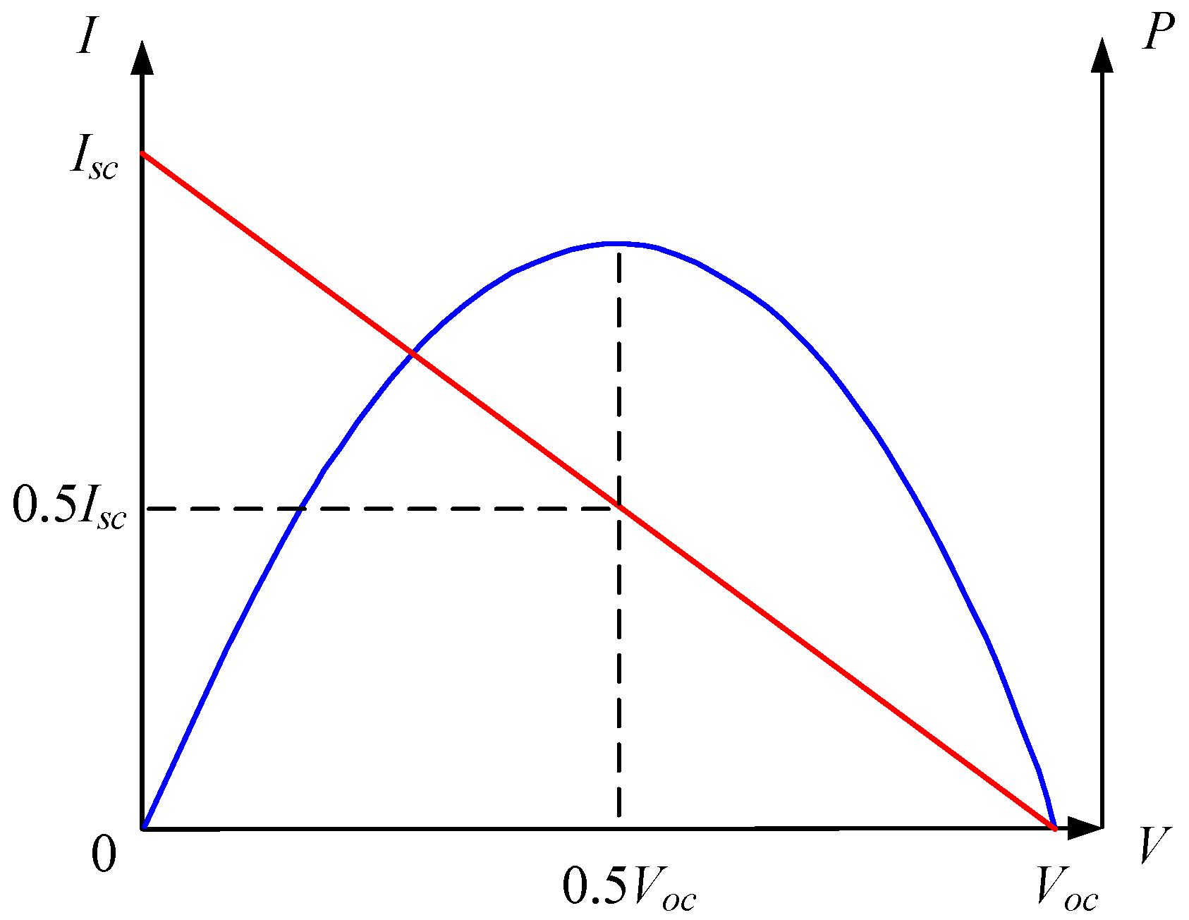
2.1. P-I-V Curve

As shown in Figure 3, the thermoelectric generator (TG) can be considered as a Thevenin equivalent circuit for analysis convenience. Voc is the open-circuit voltage at both ends of the TG; Rteg is the equivalent internal resistance; RL is the load on the TG; Vteg is the output voltage of the TG; Iteg is the output current of the TG; Isc is the short-circuit current of the TG. Accordingly, maximum power point tracking is required to obtain the maximum power transfer.
As RL is equal to Rteg, Vteg and Iteg can be shown as follows:
V t e g = V o c 2
I t e g = V o c 2 R t e g = I s c 2
From (1) and (2), the value at the maximum power point can be obtained:
P m p p = V o c 2 × I s c 2 = 1 4 V o c × I s c
Therefore, the PVI curve of the TG can be plotted by using the results of (1)–(3), as shown in Figure 4.

2.2. Measured Electrical Parameters of the used TG

Table 1 is used to describe the electrical parameters of the Marlow TG measured.

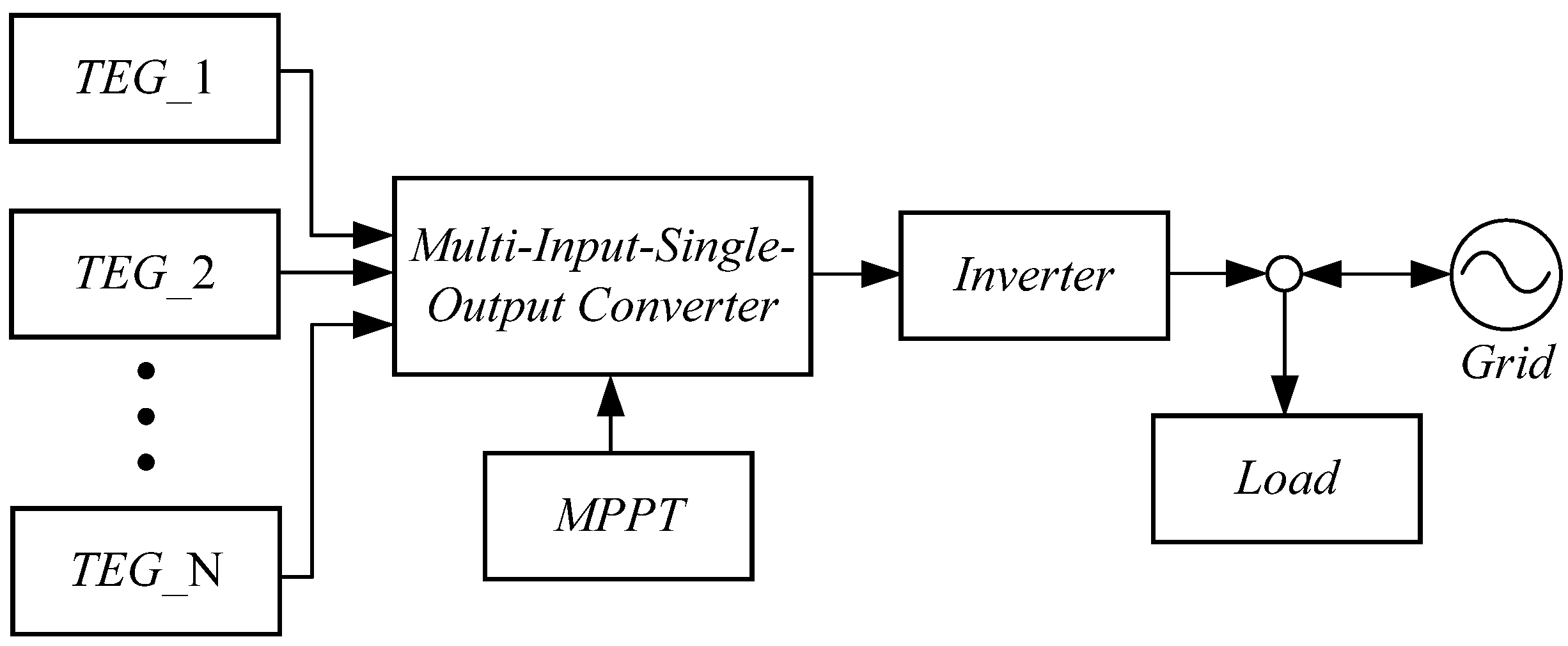
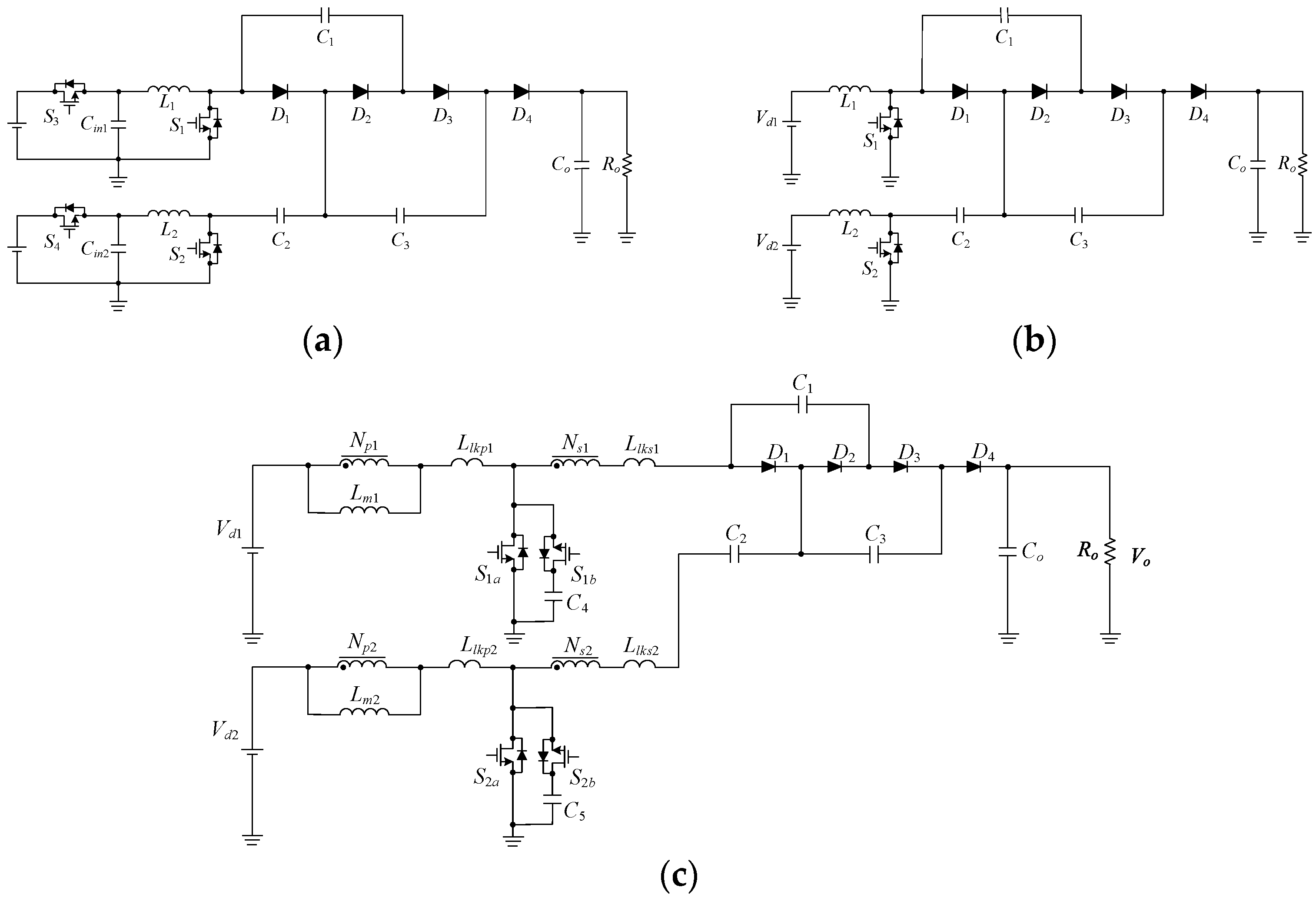
3. Proposed MISO Converter

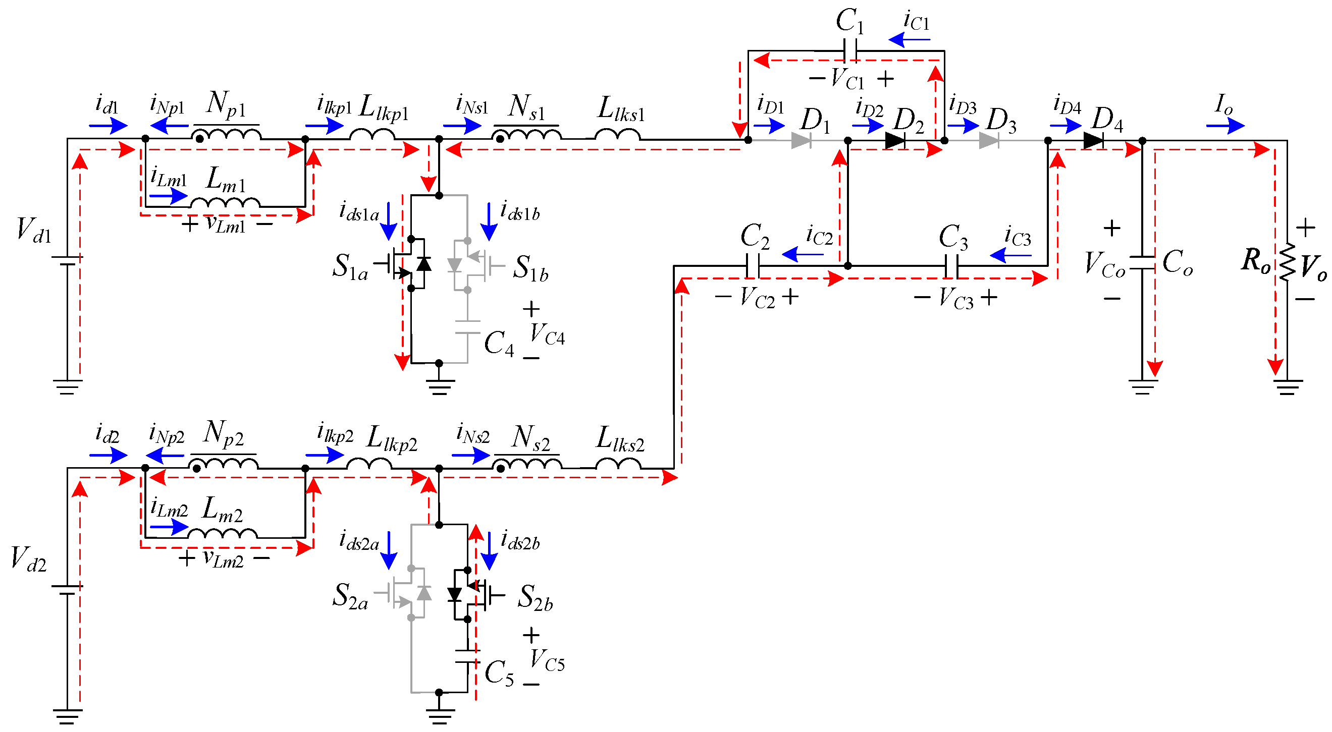
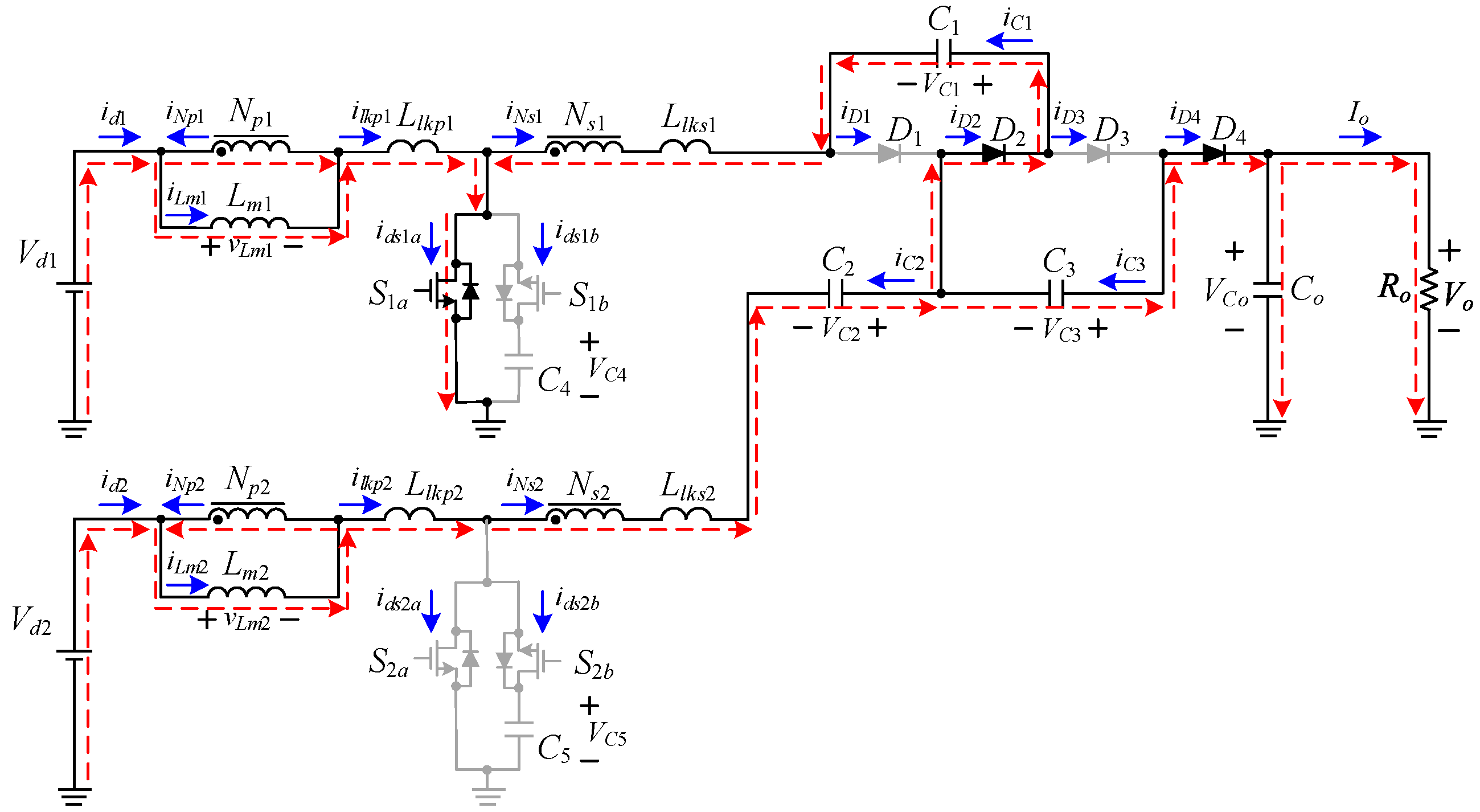
3.1. Converter Description

The circuit of the dual-input step-up converter proposed in Figure 5 consists of two input coupling inductors, four active switches S1a, S1b, S2a and S2b, two clamping capacitors C4 and C5, three energy-transferring capacitors C1, C2, and C3, four diodes D1, D2, D3, and D4, one output capacitor Co, and the load represented by the output resistor Ro.
Before proceeding with the analysis of the circuit operation, a brief explanation of the relevant symbols and the assumptions required is given.
(1)
Vd1 and Vd2 are the two input voltages; id1 and id2 are the two input currents; Io is the output current; Vo is the output voltage.
(2)
n = Ns1/Np1 = Ns2/Np2, where Np1 and Ns1 are the primary and secondary windings of the first coupling inductor, respectively and Np2 and Ns2 are the primary and secondary windings of the second coupling inductor, respectively. The currents iNp1 and iNs1 are the currents flowing through the primary and secondary windings of the first coupling inductor, respectively, whereas the currents iNp2 and iNs2 are the currents flowing through the primary and secondary windings of the second coupling inductor, respectively. The leakage inductances Llkp1, Llks1, Llkp2, and Llks2 are the primary and secondary leakage inductances of the first and second coupling inductors, respectively.
(3)
Lm1 is the magnetizing inductance of the first coupling inductor, and the voltage on and current in it are vLm1 and iLm1, respectively; Lm2 is the magnetizing inductance of the second coupling inductor, and the voltage on and current in it are vLm2 and iLm2, respectively.
(4)
The voltages vgs1a, vgs1b, vgs2a and vgs2b are the gate driving signals for the switches S1a, S1b, S2a, and S2b, respectively; the voltages vD1, vD2, vD3, and vD4 and the currents iD1, iD2, iD3, and iD4 are the voltages on and currents in the diodes D1, D2, D3, and D4, respectively.
(5)
The voltages VC1, VC2, VC3, VC4, and VC5 and the currents iC1, iC2, iC3, iC4, and iC5 are the voltages and currents in energy-transferring capacitors C1, C2, and C3 and clamping capacitors C4 and C5, respectively.
(6)
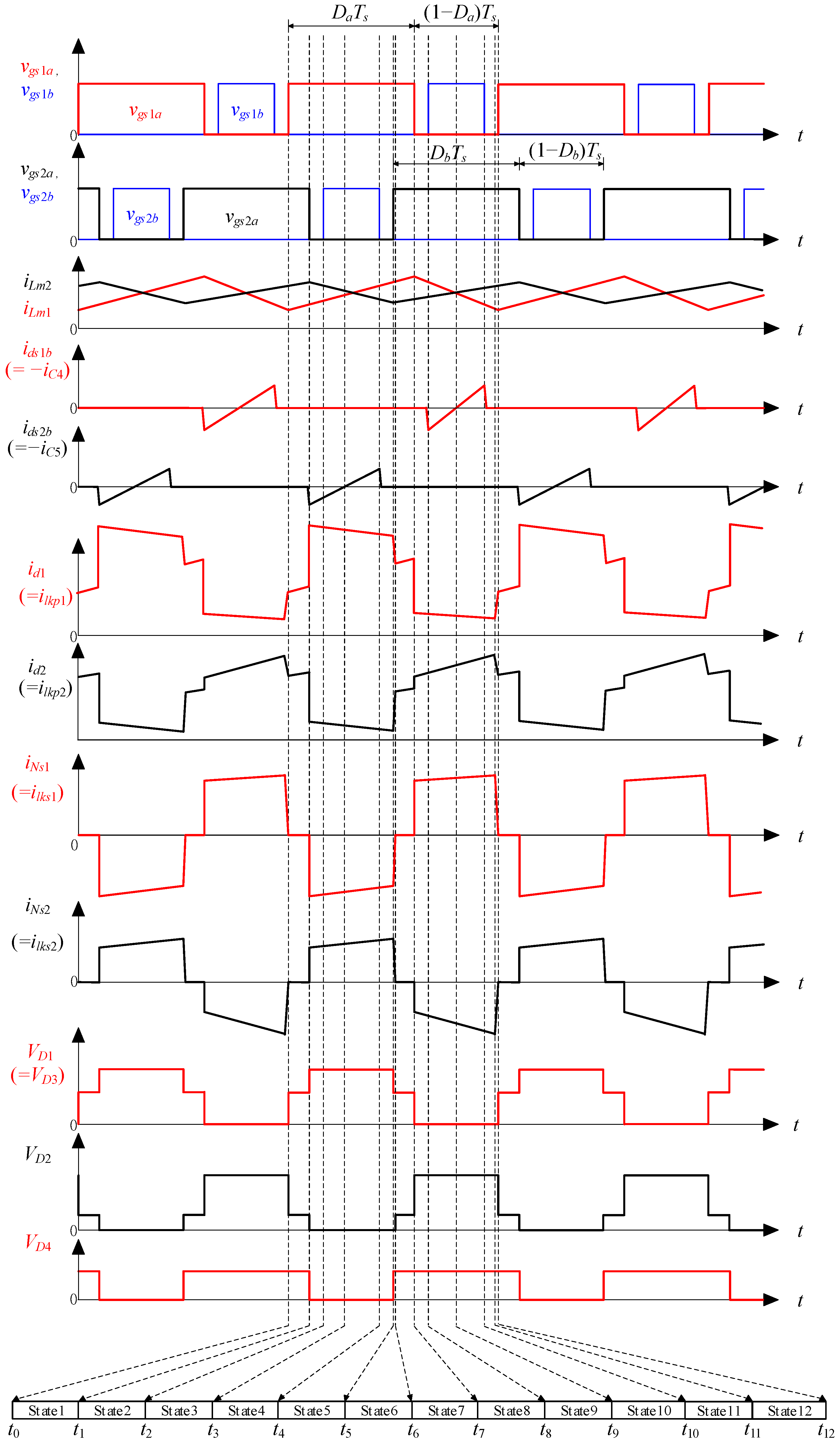
Ts is the switching period of switches S1a and S2a, and the corresponding duty cycles are Da and Db, respectively.
(7)
k1 and k2 are the coupling coefficients of the first and second coupling inductors, respectively, equal to k1 = Lm1/(Lm1 + Llkp1) and k2 = Lm2/(Lm2 + Llkp2).
(8)
L11 and L12 are the primary-side and secondary-side self-inductances of the first coupling inductor, respectively; L21 and L22 are the primary-side and secondary-side self-inductances of the second coupling inductor, respectively.
(9)
The switches, diodes, inductors, and capacitors are considered ideal components.
(10)
The circuit is operated in the continuous current mode (CCM).
(11)
All the circuit operating principles are analyzed in the steady state.
(12)
The voltage conversion ratio is derived by assuming that the voltage drops caused by the leakage inductance are ignored.
Based on the above assumptions, Figure 6 shows the illustrated waveforms associated with the proposed circuit operation.

3.2. Basic Operating Principles

3.2.1. State 1 [ t 0 t t 1 ]

As shown in Figure 7, the switches S1a and S2a are on, the switches S1b and S2b are off, and the diodes D1, D2, D3, and D4 are off. The input voltages Vd1 and Vd2 excite the magnetizing inductances Lm1 and Lm2 and the leakage inductances Llkp1 and Llkp2, whose voltages on them are k 1 V d 1 , k 2 V d 2 , 1 k 1 V d 1 , and 1 k 2 V d 2 , respectively. The reverse-biased voltage of diode D1 is V C 2 + n k 1 V d 1 k 2 V d 2 ; the reverse-biased voltage of diode D2 is V C 1 V C 2 n k 1 V d 1 k 2 V d 2 ; the reverse-biased voltage of diode D3 is V C 2 + V C 3 V C 1 + n ( k 1 V d 1 k 2 V d 2 ) ; the reverse-biased voltage of diode D4 is V o V C 2 V C 3 + n k 2 V d 2 . In addition, since all the four diodes are cut off, only the output capacitor Co releases energy to the load in this state. Once the switch S2a is turned off, state 1 comes to an end.

3.2.2. State 2 [ t 1 t t 2 ]

As shown in Figure 8, the switch S1a is on, the switches S1b, S2a, and S2b are off, the diodes D2 and D4 are on, and the diodes D1 and D3 are off. During this state, the input voltage Vd1 continues to excite the magnetizing inductance Lm1 and the leakage inductance Llkp1, whose voltages on them are k 1 V d 1 and ( 1 k 1 ) V d 1 , respectively. At the same time, the magnetizing inductance Lm2 and the leakage inductance Llkp2 are demagnetized and the voltages on them are k 2 ( V d 2 V C 5 ) and ( 1 k 2 ) ( V d 2 V C 5 ) , respectively, forcing diodes D2 and D4 to conduct. There are three key paths in this state. Path 1 is that the current ilkp2 flows through the body diode of S2b and hence the leakage inductance Llkp2 releases energy to the clamping capacitor C5; path 2 is that the energy-transferring capacitor C2 charges the energy-transferring capacitor C1 and at the same time the leakage inductance Llks1 is magnetized in the opposite direction with a voltage of n k 1 V d 1 + V C 1 + V C 3 V o ; path 3 is that the energy-transferring capacitors C2 and C3 are connected in series and release energy to the load and at the same time the leakage inductance Llks2 is magnetized with a voltage of V C 5 n k 2 ( V d 1 V C 5 ) + V C 2 + V C 3 V o . It is worth mentioning that the two coupling inductors have transformer behavior. In addition, the diode D1 is connected in parallel with the energy-transferring capacitor C1, which has a reverse-biased voltage of VC1, and the diode D3 is connected in parallel with the energy-transferring capacitor C3 and has a reverse-biased voltage of VC3, such that both the diodes D1 and D3 are cut off in this state. As the switch S2b is turned on, state 2 ends.

3.2.3. State 3 [ t 2 t t 3 ]

Before the start of state 3, the body diode of S2b is on, so S2b has zero voltage switching (ZVS) turn-on as shown in Figure 9. In addition, the energy-transferring capacitor C5 is charged with a negative slope. The moment the current iC5 reaches zero, state 3 comes to an end.

3.2.4. State 4 [ t 3 t t 4 ]

As shown in Figure 10, the switches S1a and S2b are on, the switches S1b and S2a are off, the diodes D2 and D4 are on, and the diodes D1 and D3 are off. All the components except the clamping capacitor C5 operate in the same state 3. Since the current iC5 rises in the opposite direction, the clamping capacitor C5 is discharged. Once the switch S2b is turned off, state 4 ends.

3.2.5. State 5 [ t 4 t t 5 ]

As shown in Figure 11, the switch S1a is on, the switches S1b, S2a, and S2b are off, the diodes D2 and D4 are on, and the diodes D1 and D3 are off. During this state, the input voltage Vd1 continues to excite the magnetizing inductance Lm1 and the leakage inductance Llkp1; the magnetizing inductance Lm2 and the leakage inductance Llkp2 continue to be demagnetized. As soon as the switch S2a is turned on, state 5 comes to an end.

3.2.6. State 6 [ t 5 t t 6 ]

As shown in Figure 12, the switches S1a and S2a are on, the switches S1b and S2b are off, the diode D2 is on, and the diodes D1, D3, and D4 are off. During this state, the input voltages Vd1 and Vd2 excite the magnetizing inductances Lm1 and Lm2, respectively. The leakage inductances Llks1 and Llks2 charge the energy-transferring capacitor C1 to achieve leakage inductance energy recovery.

3.2.7. State 7 [ t 6 t t 7 ]

The operation principle of this state is the same as that of state 1.

3.2.8. State 8 [ t 7 t t 8 ]

As shown in Figure 13, the switches S1a, S1b and S2b are off, and the diodes D2 and D4 are off, and the diodes D1 and D3 are on. During this state, the input voltage Vd2 continues to excite the magnetizing inductance Lm2 and the leakage inductance Llkp2, whose voltages on them are k 2 V d 2 and ( 1 k 2 ) V d 2 , respectively. At the same time, the magnetizing inductance Lm1 and the leakage inductance Llkp1 are demagnetized and the voltages on them are k 1 ( V d 1 V C 4 ) and ( 1 k 1 ) ( V d 1 V C 4 ) , respectively, forcing diodes D1 and D3 to conduct. There are three key paths: path 1 is that the current ilkp1 flows through the body diode of S1b and hence the leakage inductance Llkp1 releases energy to the clamping capacitor C4; path 2 is that the energy-transferring capacitor C1 charges the energy-transferring capacitor C3; path 3 is that the output capacitor Co releases energy to the load. It is worth mentioning that the two coupling inductors have transformer behavior. In addition, the diode D2 is connected in parallel with the energy-transferring capacitor C1 and has a reverse-biased voltage of VC1, and the diode D4 has a reverse-biased voltage of V o V C 2 V C 3 + n V d 2 , so that both the diodes D2 and D4 are cut off in this state. As the switch S1b is turned on, state 8 ends.

3.2.9. State 9 [ t 8 t t 9 ]

As shown in Figure 14, before the start of state 9, the body diode of S1b is on, so S1b has zero voltage switching (ZVS) turn-on.

3.2.10. State 10 [ t 9 t t 10 ]

As shown in Figure 15, the switches S2a and S1b are on, switches S1a and S2b are off, diodes D1 and D3 are on, and diodes D2 and D4 are off. All the components except the clamping capacitor C4 operate in the same state 9. Since the current iC4 rises in the opposite direction, the clamping capacitor C4 is discharged. Once the switch S1b is turned off, state 10 ends.

3.2.11. State 11 [ t 10 t t 11 ]

As shown in Figure 16, the switch S2a is on, the switches S1a, S1b, and S2b are off, the diodes D1 and D3 are on, and the diodes D2 and D4 are off. At the same time, the input voltage Vd2 continues to excite the magnetizing inductance Lm2 and the leakage inductance Llkp2; the magnetizing inductance Lm1 and the leakage inductance Llkp1 continue to be demagnetized. As soon as S1a is turned on, state 11 comes to an end.

3.2.12. State 12 [ t 11 t t 12 ]

As shown in Figure 17, the switches S1a and S2a are on, the switches S1b and S2b are off, the diode D1 is on, and the diodes D2, D3, and D4 are off. At the same time, the input voltages Vd1 and Vd2 excite the magnetizing inductances Lm1 and Lm2, respectively. The leakage inductances Llks1 and Llks2 charge the energy-transferring capacitor C2 to achieve leakage inductance energy recovery.

3.3. Voltage Conversion Ratio

To facilitate the derivation of the voltage conversion ratio and voltages across the energy-transferring capacitors C1, C2, and C3, only states 1, 4, and 8 are considered. In addition, the blanking times of the switches, the primary-side leakage inductances Llkp1 and Llkp2, and the secondary-side leakage inductance Llks1 and Llks2 are ignored.
n = N s 1 N p 1 = N s 2 N p 2
From state 1 shown in Figure 7, the expressions for the voltages on Lm1 and Lm2 are as follows:
v L m 1 = V d 1
v L m 2 = V d 2
From state 4 shown in Figure 10, the expression for the voltage on Lm1 is the same as that state 1 but the voltage on Lm2 is as follows:
v L m 2 = V d 2 V C 5
Additionally, the expressions for the voltages VC1, VC5, and Vo can be expressed as
V C 1 = V C 5 n ( V d 2 V C 5 ) + V C 2 + n V d 1
V o = V C 5 n ( V d 2 V C 5 ) + V C 2 + V C 3
V C 5 = V d 2 1 D b
On the other hand, from state 9 shown in Figure 14, the expression for the voltage on Lm2 is the same as that for state 1 but the voltage on Lm1 is as below:
v L m 1 = V d 1 V C 4
At the same time, the voltages on C2, C1, and C4 are given by
V C 2 = V C 4 n ( V d 1 V C 4 ) + n V d 2
V C 1 = V C 3
V C 4 = V d 1 1 D a
By substituting (14) into (12), the expression for VC2 is given by
V C 2 = ( n + 1 ) V d 1 1 D a + n ( V d 2 V d 1 )
By substituting (10) and (12) into (8), the expression for VC1 can be obtained as
V C 1 = ( n + 1 ) 1 D a V d 1 + ( n + 1 ) 1 D b V d 2
By substituting Equations (10), (12)–(14), and (16) into Equation (9), the output voltage Vo is given by
V o = 2 + n ( 1 + D a ) 1 D a V d 1 + 2 ( 1 + n ) 1 D b V d 2

3.4. Unequal Currents between the Two Inputs

This subsection will show that the proposed structure has an automatic current sharing element embedded but does not have an automatic current sharing feature. To simplify the analysis, it is assumed that there is no loss in power conversion in this circuit, i.e., the input power is equal to the output power. According to (17), the power of the two inputs can be split and their DC output currents can be assumed to be the same, equal to Io.
As shown in Figure 5, the input currents Id1 and Id2 can be expressed as
I d 1 = I L m 1 I N p 1
I d 2 = I L m 2 I N p 2
Next, the DC component of the coupling inductor is analyzed. According to the ampere-second balance, the average current in the capacitor is zero, so the following equations can be obtained as follows:
I N p 1 = N s 1 N p 1 × I N s 1 = N s 1 N p 1 × I o = n I o
I N s 2 = I N p 2 = 0
By substituting (18) into (20), the expression for the current Id1 can be obtained as
I d 1 = I L m 1 n I o
Additionally, substituting (19) into (21) yields the expression for current Id2 as
I d 2 = I L m 2
Because there is no loss of power conversion in the circuit, the following equation can be obtained as
V o I o = V d 1 I d 1 + V d 2 I d 2
and also, multiplying (17) by Io yields
V o I o = 2 + n ( 1 + D a ) 1 D a V d 1 I o + 2 ( 1 + n ) 1 D b V d 2 I o
By comparing (24) and (25) to find the relationship between the input currents Id1 and Id2 and the output current Io, the following Equations (22) and (23) can be obtained as
I d 1 = 2 + n ( 1 + D a ) 1 D a I o = I L m 1 n I o
I d 2 = 2 ( 1 + n ) 1 D b I o = I L m 2
From (26), ILm1 can be obtained as
I L m 1 = 2 ( 1 + n ) 1 D a I o
By substituting (23) and (26) into (18) and (19), the DC components of the input currents can be found as
I d 1 = 2 ( 1 + n ) 1 D a I o n I o
I d 2 = 2 ( 1 + n ) 1 D b I o
The two input currents will not be identical even if Da is equal to Db, according to (29) and (30).

3.5. Extension of Number of Phases

The number of phases can be extended by 2N, where N is a positive integer. Figure 18 shows the four-phase interleaved converter.

4. Hardware Circuit Design

4.1. Thermoelectric Module Specifications

The thermoelectric generator (TG), namedTG12-8, is manufactured by Marlow Industries, Inc. Since this converter has two inputs, the first input is composed of four pieces of TGs connected in series, and the second input is composed of two pieces of TGs connected in series. Table 2 shows the associated information on the first thermoelectric module and Table 3 shows the associated information on the second thermoelectric module. Figure 19 and Figure 20 show the measured curves for the first and second thermoelectric modules, respectively. These measured curves for the two thermoelectric modules are based on the Prodigit 9842-MPPT function under constant voltage mode, sweeping so as to obtain the data relevant to power vs. voltage (PV) and voltage vs. voltage (IV), and then plotting these data by using Microsoft Excel.
As can be seen from Figure 19, the maximum power point of the first TG has 18.52 W at half of the open-circuit voltage and short-circuit current of the first thermoelectric module, with values of Vmpp1 = 16.22 V and Impp1 = 1.145 A. As can be seen from Figure 20, the maximum power point of the second thermoelectric module has 9W at half of the open-circuit voltage and short-circuit current of the second thermoelectric module, with values of Vmpp2 = 7.67 V and Impp2 = 1.177 A.

4.2. System Configuration and Its Specifications

Figure 21 shows the system configuration of the proposed circuit applied to a thermoelectric conversion system with two thermoelectric modules at individual inputs. The main power stage is a dual-input high-boost circuit with a digital control kernel based on FPGA to control the system. The FPGA calculates and then sends the duty cycles to the gate drivers to achieve the maximum power tracking. For the voltages and currents to be sampled, analog-to-digital converters (ADCs) are used. The sensed signals are sent to MPPT modules after ADCs via FPGA-embedded series peripheral interfaces (SPIs). Furthermore, the voltage-sensing resistors are used as voltage dividers, the current-sensing resistors are used as current sensors, and the FPGA, named CycloneEP1C3T100, is used as a control kernel, which needs a 20 MHz oscillator and has 2910 logic gates, 104 I/O ports, 59,904 RAM bits, and a phase-lock loop. In addition, the design software is based on the very high-speed hardware description language (VHDL) and Table 4 shows the system specifications.

4.3. Voltage Stresses of Switches and Diodes

The voltage across the switches S1a and S1b during the turn-off period can be found from states 9 and 1, respectively, as follows:
V d s 1 a = V d s 1 b = V C 4 = V d 1 1 D a = 16.22 1 0.575 = 38.17 V
The voltages across the switches S2a and S1b during the turn-off period are given by states 3 and 1, respectively, as follows:
V d s 2 a = V d s 2 b = V C 5 = V d 2 1 D b = 7.67 1 0.572 = 18 V
In state 2, the voltage across diodes D1 and D3 are as follows:
V D 1 = V C 1
V D 3 = V C 3
Substituting the results of (13) and (16) into (33) and (34) yields
V C 1 = V C 3 = ( n + 1 ) 1 D a V d 1 + ( n + 1 ) 1 D b V d 2 = 224.34 V
The voltages across the diodes D2 and D4 in state 8 are as follows:
V D 2 = V C 1 = 224 . 34 V
V D 4 = V o V C 2 V C 3 + n V d 2 = 71.4 V

4.4. Component Specifications

Table 5 is used to describe the specifications of the used components.

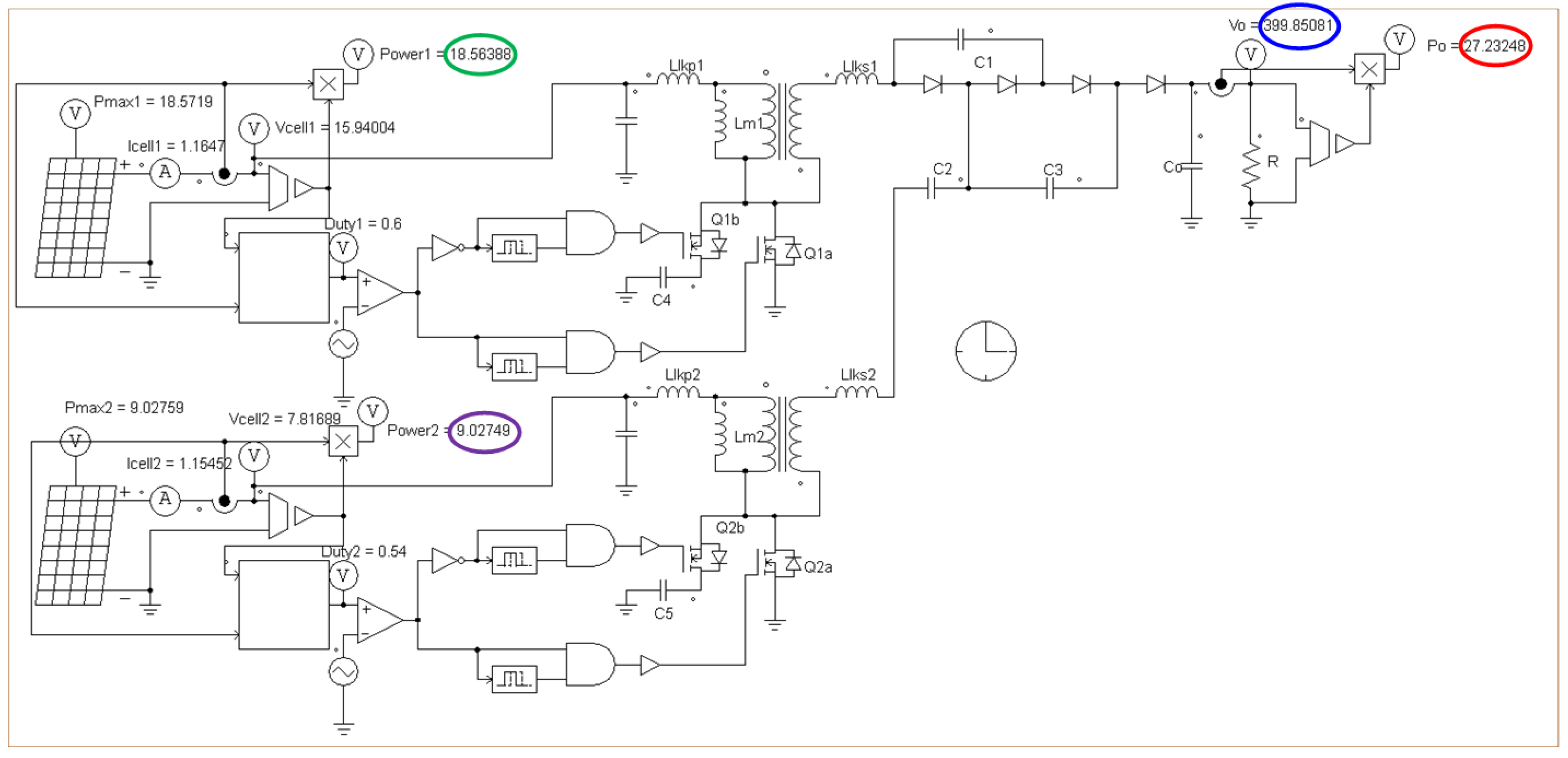
5. Maximum Power Point Tracking

5.1. MPPT Algorithm

If a thermoelectric module is to provide maximum power output in different temperature ranges and temperature differences, maximum power tracking is required to operate the thermoelectric module at the maximum power point. In addition, the PV characteristic curve of a thermoelectric module is similar to that of a solar cell. However, the difference between them is that the PV characteristic curve of a thermoelectric module is more symmetrical. Consequently, according to this feature, a maximum power tracking method based on three-point-weighting MPPT is relatively suitable for thermoelectric modules in practice.
Figure 22 shows the MPPT flow chart used in this paper. The principle of this control method is to calculate the power value by continuously detecting the output power value at three points and comparing their power magnitudes. First of all, set a duty cycle of Db at the reference point b, and detect the output voltage and current of the thermoelectric module to calculate the power value Pb; sequentially, increase the duty cycle by one unit of disturbance, i.e., D b + Δ D , to obtain the second duty cycle of Dc at the point c, and detect and calculate the power value of Pc; then reduce the duty cycle by one unit of disturbance, i.e., D b Δ D , to obtain the third duty cycle of Da at the point a, and detect and calculate the power value of Pa. By doing so, the power sampling procedure is completed. Afterwards, if the power Pa is greater than or equal to the power Pb, the weight value of W1 will be increased by one, and if not, the weight value of W1 will be decreased by one; if the power Pb is greater than or equal to the power Pa, the weight value of W2 will be increased by one, and if not, the weight value of W2 will be decreased by one. Eventually, calculate the weight value to determine the direction of movement of the reference point. If the sum of W1 and W2 is + 2 , then the point c is used as the new reference point with the duty cycle of Dc; if the sum of W1 and W2 is 2 , the point a is used as the new reference point with the duty cycle of Da; if the sum of W1 and W2 is 0, then the reference point b remains unchanged with the duty cycle of Db. After completing the above actions, the weight value is returned to zero and the above actions are repeated to achieve maximum power point tracking.

5.2. MPPT Simulation

In this subsection, the simulation of the proposed MISO circuit applied to a thermoelectric conversion system is used to verify its feasibility based on the power simulation (PSIM) software. Therefore, the simulation environment is constructed by analog devices as shown in Figure 23. From this figure, it can be seen that both thermoelectric modules can be traced to individual maximum power points without need of staggered switching; the first thermoelectric module outputs 18.56 W shown in a green circle, almost corresponding to18.52 W, shown in Table 2; the second thermoelectric module outputs 9.03 W, shown in the purple circle, almost corresponding to 9 W shown in Table 3; both the two thermoelectric modules output 27.23 W shown in the red circle, almost corresponding to 27.51 W, shown in Table 4; the output voltage can be increased to 399.85 V, shown in a blue circle, almost corresponding to 400 V, shown in Table 4.

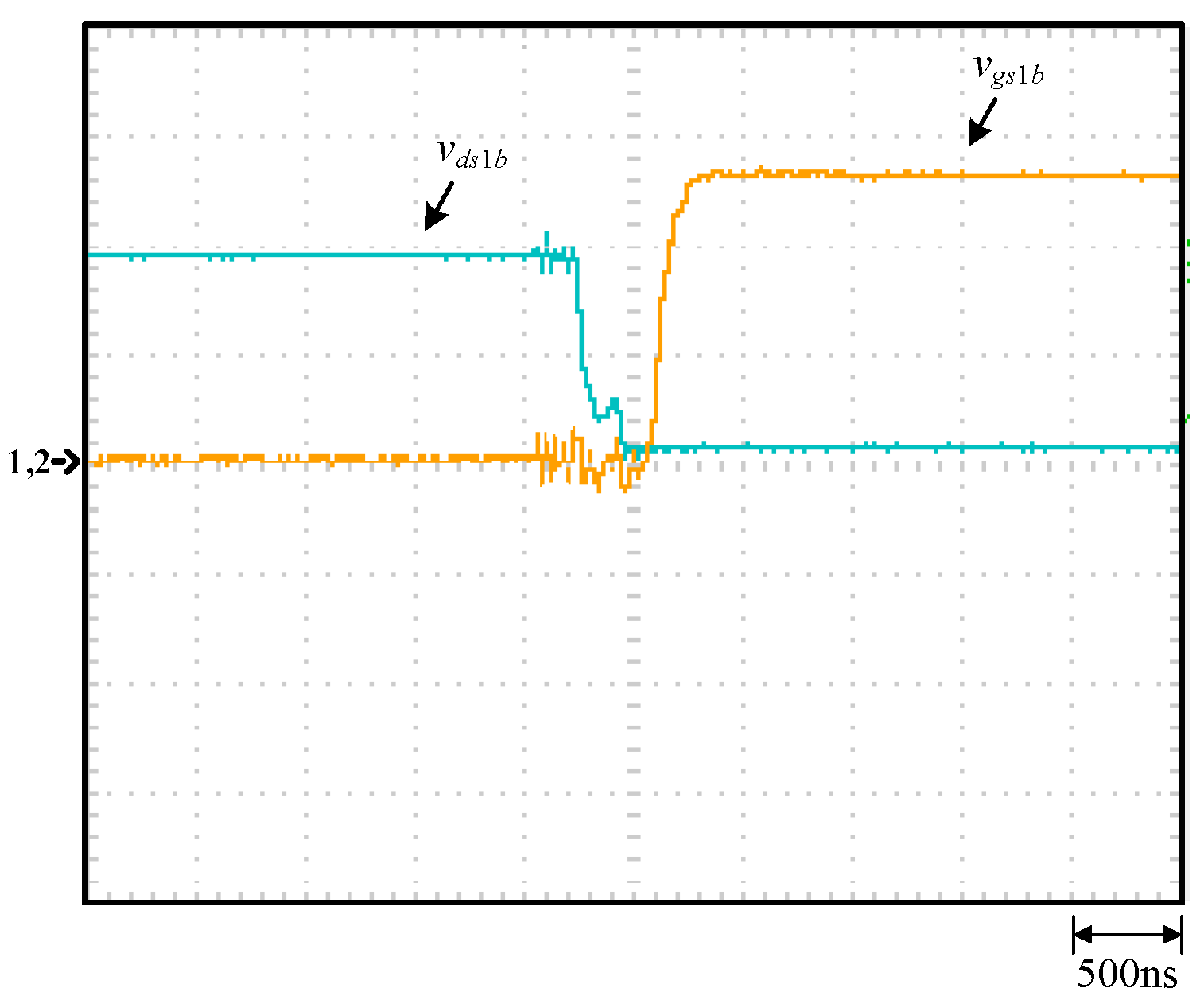
6. Experimental Results

In this subsection, the experimental results are used to demonstrate the effectiveness of the proposed MISO circuit. The digital control kernel based on the FPGA is adopted herein. From Figure 24, it can be seen that the gate driving signals vgs1a and vgs2a are interleaved and vgs1b and vgs2b are complementary to vgs1a and vgs2a, respectively. From Figure 25 and Figure 26, it can be seen that when the switches S1a, S1b, S2a, and S2b are turned off, the leakage inductance of the coupling inductor, the parasitic inductance on the line, and the parasitic capacitance of the switch resonate together, so the voltage spike and ring on vds1a, vds1b, vds2a, and vds2b will be generated. As shown in Figure 27, the resonance of the leakage inductance with the diode capacitance from state 6 to state 7 and from state 12 to state 1 causes the current spike and oscillation in the input currents id1 and id2 due to the reverse recover current of the diode D1. As can be seen from Figure 28, the energy-transferring capacitors C1, C2, and C3 can be stabilized at a certain value for any load. Figure 29 and Figure 30 show that the switches S1b and S2b have ZVS turn-on but are turned on with the resonance between the diode capacitance and the leakage inductance, thereby yielding the voltage spike and oscillation on vds1b and vds2b. From Figure 31, it can be seen that the diodes D1 and D3 have the same operating behavior and the oscillation is caused by the magnetizing inductance resonating with the diode capacitance. From Figure 32, it can be seen that the output voltage Vo of the proposed circuit can reach 400 V. From Figure 33, it can be seen that the efficiency can be up to 89.27% at 100% load. Figure 34 shows a photo of the experimental setup.

7. Conclusions

In this paper, the interleaved MISO circuit was applied to a thermoelectric system, where the ultrahigh voltage gain was obtained by using coupling inductors and switched capacitors. The two thermoelectric modules have individual MPPTs even although the passive current-sharing device is embedded in this circuit, and this was verified by Section 3.4. Furthermore, the active voltage clamp circuits ensure that the high-frequency oscillation is reduced, the switches are turned on with ZVS, and that the voltage stresses on the switches are low. Therefore, the rated-load efficiency is 89.27%. In addition, the number of inputs can be extended.

Author Contributions

Conceptualization, K.-I.H. and J.-J.S.; methodology, K.-I.H. and J.-J.S.; software, P.-J.C.; validation, J.-J.S.; formal analysis, P.-J.C.; investigation, P.-J.C.; resources, K.-I.H.; data curation, P.-J.C.; writing—original draft preparation, K.-I.H.; writing—review and editing, K.-I.H.; visualization, J.-J.S.; supervision, K.-I.H.; project administration, K.-I.H.; funding acquisition, K.-I.H. All authors have read and agreed to the published version of the manuscript.

Funding

This research was funded by the Ministry of Science and Technology, Taiwan, under the Grant Number: MOST 110-2221-E-027-045-MY2.

Institutional Review Board Statement

Not applicable.

Informed Consent Statement

Not applicable.

Data Availability Statement

No new data were created or analyzed in this study. Data sharing is not applicable to this article.

Conflicts of Interest

The authors declare no conflict of interest.

References

  1. Arshadi, S.A.; Poorali, B.; Adib, E.; Farzanehfard, H. High step-up DC-AC inverter suitable for AC module applications. IEEE Trans. Ind. Electron. 2016, 63, 832–839. [Google Scholar] [CrossRef]
  2. Taghvaie, A.; Adabi, J.; Rezanejad, M. Circuit topology and operation of a step-up multilevel inverter with a single DC source. IEEE Trans. Ind. Electron. 2016, 63, 6643–6652. [Google Scholar] [CrossRef]
  3. Akar, F.; Kale, M. A high voltage gain multi-input converter. In Proceedings of the 2018 2nd International Symposium on Multidisciplinary Studies and Innovative Technologies (ISMSIT) (IEEE ISMSIT’18), Ankara, Turkey, 19–21 October 2018; pp. 1–4. [Google Scholar]
  4. Varesi, K.; Hosseini, S.H.; Sabahi, M.; Babaei, E. A multi-port high step-up DC-DC converter with reduced normalized voltage stress on switches/diodes. In Proceedings of the 9th Annual Power Electronics, Drives Systems and Technologies Conference (IEEE PEDSTC’18), Tehran, Iran, 13–15 February 2018; pp. 1–6. [Google Scholar]
  5. Khwan-on, S.; Kongkanjana, K. The control of a multi-input boost converter for renewable energy system applications. In Proceedings of the 2017 International Electrical Engineering Congress (IEEE IEECON’16), Pattaya, Thailand, 8–10 March 2017; pp. 1–4. [Google Scholar]
  6. Irmak, E.; Guler, N. Application of a boost based multi-input single-output dc/dc converter. In Proceedings of the 2017 IEEE 6th International Conference on Renewable Energy Research and Applications (IEEE ICRERA’17), San Diego, CA, USA, 5–8 November 2017; pp. 955–961. [Google Scholar]
  7. Mohammadi, M.; Safari, N.; Milimonfared, J.; Moghani, J.S. Application of a new high step-up double-input converter in a novel module-integrated-inverter photovoltaic system. In Proceedings of the 6th Power Electronics, Drive Systems & Technologies Conference (IEEE PEDSTC’15), Tehran, Iran, 3–4 February 2015; pp. 53–58. [Google Scholar]
  8. Khosravi, M.; Khaburi, D.A.; Heshmatian, S. Predictive control of multi-input switched-capacitor DC-DC converter with reduced switching frequency. In Proceedings of the 8th Power Electronics, Drive Systems & Technologies Conference (IEEE PEDSTC’17), Mashhad, Iran, 14–16 February 2017; pp. 549–554. [Google Scholar]
  9. Hwu, K.-I.; Jiang, W.-Z. Analysis, design and derivation of a two-phase converter. IET Power Electron. 2015, 8, 1987–1995. [Google Scholar] [CrossRef]
  10. Gorji, S.A.; Ektesabia, M.; Zheng, J. Double-input boost/y-source DC-DC converter for renewable energy sources. In Proceedings of the 2nd Annual Southern Power Electronics Conference (IEEE SPEC’16), Auckland, New Zealand, 5–8 December 2016; pp. 1–6. [Google Scholar]
  11. Mummadi, V.; Sawant, K.K. Control of multi-input integrated buck-boost converter. In Proceedings of the IEEE Region 10 and the Third International Conference on Industrial and Information Systems, Kharagpur, India, 8–10 December 2008; pp. 1–6. [Google Scholar]
  12. Suetomi, M.; Matsuo, H.; Hirakida, K.; Nakashima, R.; Hamaguchi, R.; Yoichi, I.; Lin, W. A novel multi-input DC-DC converter with high power efficiency. In Proceedings of the 33rd International Telecommunications Energy Conference (IEEE INTELEC’11), Amsterdam, The Netherlands, 9–13 October 2011; pp. 1–5. [Google Scholar]
  13. Haghighian, S.K.; Tohidi, S.; Feyzi, M.R.; Sabahi, M. Design and analysis of a novel SEPIC-based multi-input DC/DC converter. IET Power Electron. 2017, 10, 1393–1402. [Google Scholar] [CrossRef]
  14. Kallukaran, C.; Unnikrishnan, L. Multi-input interleaved DC-DC converter with low current ripple for electric vehicle application. In Proceedings of the 2018 International Conference on Current Trends towards Converging Technologies (IEEE ICCTCT’18), Coimbatore, India, 1–3 March 2018; pp. 1–5. [Google Scholar]
  15. Sathyan, S.; Suryawanshi, H.M.; Shitole, A.B.; Ballal, M.S.; Borghate, V.B. Soft-switched interleaved DC/DC converter as front-end of multi-inverter structure for micro grid applications. IEEE Trans. Power Electron. 2018, 33, 7645–7655. [Google Scholar] [CrossRef]
  16. Faraji, R.; Farzanehfard, H. Soft-switched non-isolated high step-up three-port dc–dc converter for hybrid energy systems. IEEE Trans. Power Electron. 2018, 33, 10101–10111. [Google Scholar] [CrossRef]
  17. Park, J.-H.; Kim, J.-K. A non-isolated dual-input DC-DC converter with wide input voltage range for renewable energy sources. In Proceedings of the 2017 IEEE 3rd International Future Energy Electronics Conference and ECCE Asia (IEEE IFEEC’17), Kaohsiung, Taiwan, 3–7 June 2017; pp. 654–658. [Google Scholar]
  18. Wang, Y.; Han, F.; Yang, L.; Xu, R.; Liu, R. A three-port bidirectional multi-element resonant converter with decoupled power flow management for hybrid energy storage systems. IEEE Access 2018, 6, 61331–61341. [Google Scholar] [CrossRef]
  19. Athikkal, S.; Kumar, G.G.; Sundaramoorthy, K.; Sankar, A. Performance analysis of novel bridge type dual input DC-DC converters. IEEE Access 2017, 5, 15340–15353. [Google Scholar] [CrossRef]
  20. Yau, Y.T.; Hwu, K.I.; Shieh, J.J. Development of a thermal energy harvesting converter with multiple inputs and an isolated output. Energies 2022, 15, 273. [Google Scholar] [CrossRef]
  21. Hwu, K.I.; Yau, Y.T.; Hsieh, M.L. Thermoelectric energy conversion system with multiple input. IEEE Trans. Power Electron. 2020, 35, 1603–1621. [Google Scholar] [CrossRef]
Figure 1. Block diagram of a thermoelectric system with multiple inputs.
Applsci 13 05692 g001
Figure 2. Interleaved MISO converter: (a) modified [21]; (b) existing [9]; (c) proposed.
Applsci 13 05692 g002
Figure 3. Thermoelectric generator: (a) Thevenin equivalent circuit; (b) open-circuit test; (c) short-circuit test.
Applsci 13 05692 g003
Figure 4. Curves for the TG: (1) blue line for P-V; (2) red line for I-V.
Applsci 13 05692 g004
Figure 5. Proposed MISO circuit with current and voltage symbols defined.
Applsci 13 05692 g005
Figure 6. Illustrated waveforms associated with the proposed circuit operating.
Applsci 13 05692 g006
Figure 7. Circuit operation for state 1.
Applsci 13 05692 g007
Figure 8. Circuit operation for state 2.
Applsci 13 05692 g008
Figure 9. Circuit operation for state 3.
Applsci 13 05692 g009
Figure 10. Circuit operation for state 4.
Applsci 13 05692 g010
Figure 11. Circuit operation for state 5.
Applsci 13 05692 g011
Figure 12. Circuit operation for state 6.
Applsci 13 05692 g012
Figure 13. Circuit operation for state 8.
Applsci 13 05692 g013
Figure 14. Circuit operation for state 9.
Applsci 13 05692 g014
Figure 15. Circuit operation of state 10.
Applsci 13 05692 g015
Figure 16. Circuit operation for state 11.
Applsci 13 05692 g016
Figure 17. Circuit operation for state 12.
Applsci 13 05692 g017
Figure 18. Four-input single-output interleaved high step-up converter.
Applsci 13 05692 g018
Figure 19. Curves for the first thermoelectric module: (1) blue line for P-V; (2) orange line for I-V.
Applsci 13 05692 g019
Figure 20. Curves for the second thermoelectric module: (1) blue line for P-V; (2) orange line for I-V.
Applsci 13 05692 g020
Figure 21. System configuration.
Applsci 13 05692 g021
Figure 22. Flow chart of the three-point-weighting MPPT.
Applsci 13 05692 g022
Figure 23. Simulation of the proposed MISO circuit applied to a thermoelectric conversion system.
Applsci 13 05692 g023
Figure 24. Measured waveforms relevant to gate driving signals: (1) vgs1a; (2) vgs1b; (3) vgs2a; (4) vgs2b.
Applsci 13 05692 g024
Figure 25. Measured waveforms relevant to S1a and S1b: (1) vgs1a; (2) vds1a; (3) vgs1b; (4) vds1b.
Applsci 13 05692 g025
Figure 26. Measured waveforms relevant to S2a and S2b: (1) vgs2a; (2) vds2a; (3) vgs2b; (4) vds2b.
Applsci 13 05692 g026
Figure 27. Measured waveforms relevant to two input currents: (1) vgs1a; (2) vgs2a; (3) id1; (4) id2.
Applsci 13 05692 g027
Figure 28. Measured waveforms relevant to voltages across capacitors: (1) VC1; (2) VC2; (3) VC3.
Applsci 13 05692 g028
Figure 29. Zoomed-in waveforms of Figure 25 relevant to S1b: (1) vgs1b; (2) vds1b.
Applsci 13 05692 g029
Figure 30. Zoomed-in waveforms of Figure 26 relevant to S2b: (1) vgs2b; (2) vds2b.
Applsci 13 05692 g030
Figure 31. Measured waveforms relevant to diodes: (1) vD1; (2) vD2; (3) vD3; (4) vD4.
Applsci 13 05692 g031
Figure 32. Measured waveforms relevant to input and output voltages: (1) Vd1; (2) Vd2; (3) Vo.
Applsci 13 05692 g032
Figure 33. Curve of efficiency vs. load current.
Applsci 13 05692 g033
Figure 34. Photo of the experimental setup.
Applsci 13 05692 g034
Table 1. Measured electrical parameters of the Marlow TG.
Electrical ParameterValue
Maximum power point voltage (TC = 80 °C/TH = 250 °C)4.05 V
Maximum power point current (TC = 80 °C/TH = 250 °C)1.15 A
Maximum power (TC = 80 °C/TH = 250 °C)3.1 W
Table 2. Specifications of the first thermoelectric module.
First thermoelectric Module SpecificationName or Value
TG product nameTG12-8
TG size 40 × 40 × 3.2 mm
Number of TGs4 in series
Max. Power @ MPP (Pmpp1)18.52 W
Voltage @ MPP (Vmpp1)16.22 V
Current @ MPP (Impp1)1.145 A
Open-circuit voltage (Voc1)30.26 V
Short-circuit current (Isc1)2.43 A
Cold-side temperature80 °C
Hot-side temperature250 °C
Table 3. Specifications of the second thermoelectric module.
Second Thermoelectric Module SpecificationName or Value
TG product nameTG12-8
TG size 40 × 40 × 3.2 mm
Number of TGs2 in series
Max. Power @ MPP (Pmpp2)9 W
Voltage @ MPP (Vmpp2)7.67 V
Current @ MPP (Impp2)1.177 A
Open-circuit voltage (Voc2)14.07 V
Short-circuit current (Isc2) 2.46 A
Cold-side temperature80 °C
Hot-side temperature250 °C
Table 4. System specifications.
System SpecificationName or Value
System operation modeContinuous conduction mode (CCM)
First input voltage (Vd1)16.22 V
Second input voltage (Vd2)7.67 V
Rated output voltage (Vo)400 V
Rated output current (Io,rated)/power (Po,rated)68.8 mA/27.52 W
Minimum output current (Io,min)/power (Po,min)17.2 mA/6.88 W
First duty cycle (Da)0.575
Second duty cycle (Db)0.572
First duty frequency (fs)/period (Ts)100 kHz/10 μs
Table 5. Component specifications.
ComponentSpecification
MOSFET switches S1a, S1b, S2a, S2bIRF3205Z
Diodes D1, D2, D3SFF1008G
Diodes D4STPS20H100CT
Energy-transferring capacitors C1, C3100 μF Electrolytic Capacitor
Energy-transferring capacitor C268 μF Electrolytic Capacitor
Clamping capacitors C4, C510 μF Electrolytic Capacitor
Output capacitor Co22 μF Electrolytic Capacitor
Coupling inductor 1/Coupling inductor 2Lm1 = 365.6 μH, n = 3/Lm2 = 87.3 μH, n = 3
Isolated gate driverFOD3182
Disclaimer/Publisher’s Note: The statements, opinions and data contained in all publications are solely those of the individual author(s) and contributor(s) and not of MDPI and/or the editor(s). MDPI and/or the editor(s) disclaim responsibility for any injury to people or property resulting from any ideas, methods, instructions or products referred to in the content.

