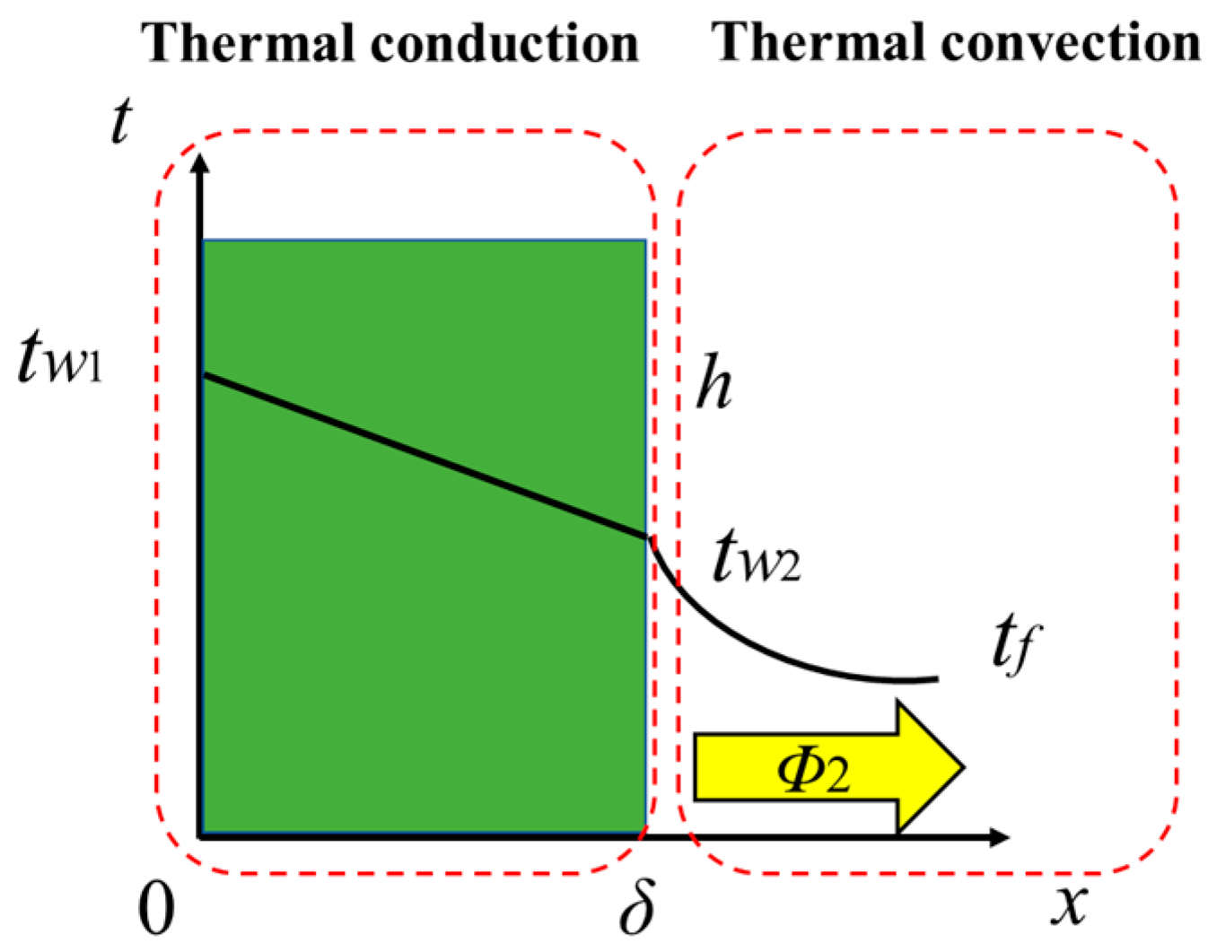
Figure 1.
Thermal transfer.
Figure 1.
Thermal transfer.
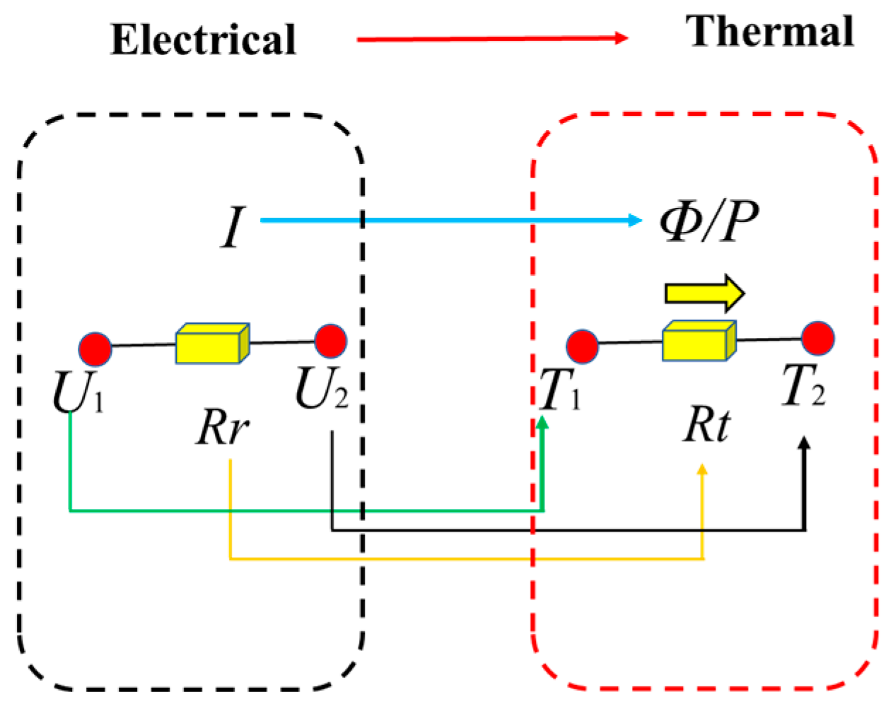
Figure 2.
The theory of electrical to thermal.
Figure 2.
The theory of electrical to thermal.
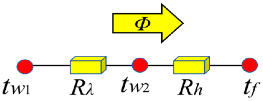
Figure 3.
Thermal resistance network.
Figure 3.
Thermal resistance network.
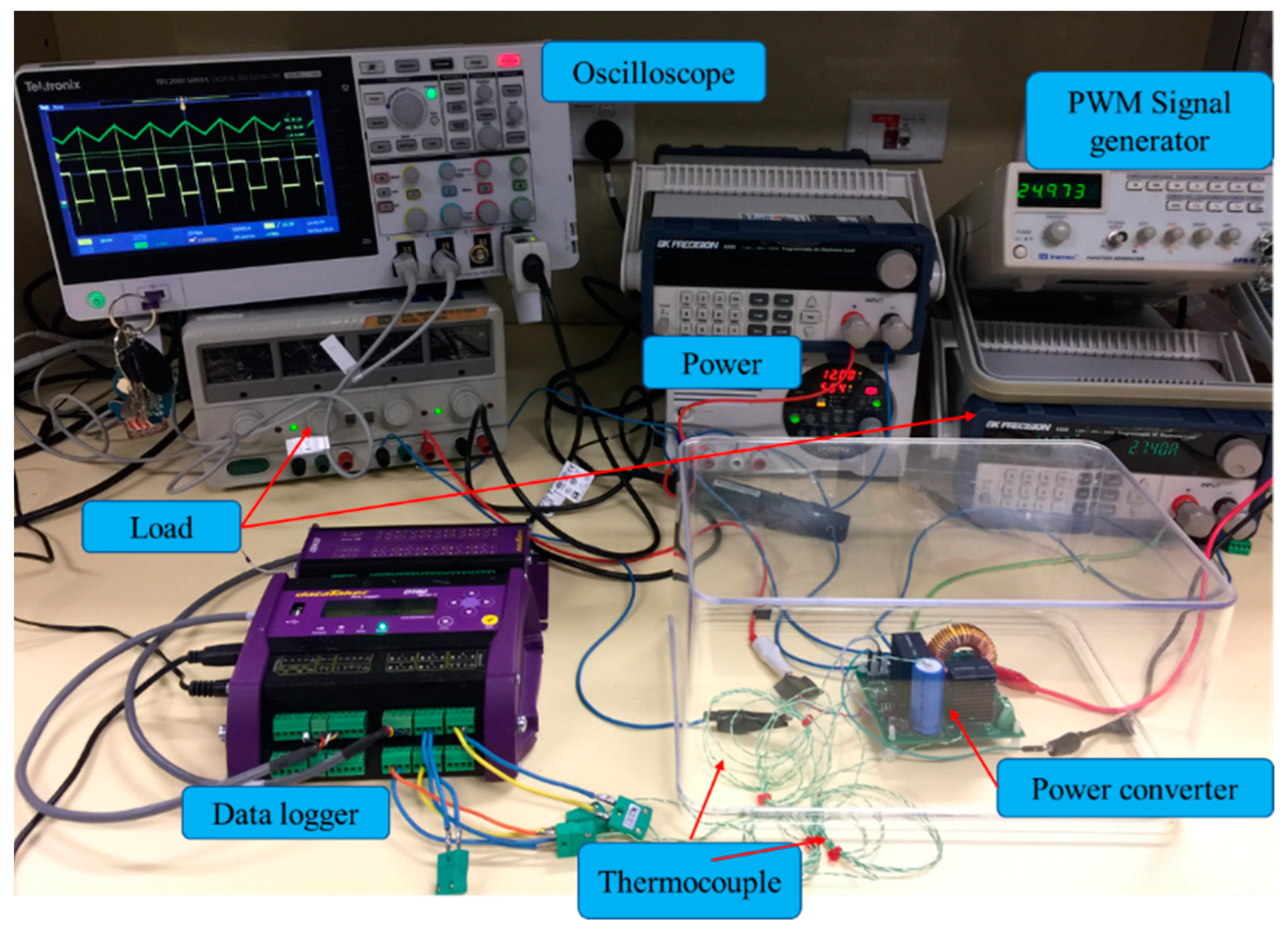
Figure 4.
Thermal coupling testing platform of the power converter.
Figure 4.
Thermal coupling testing platform of the power converter.
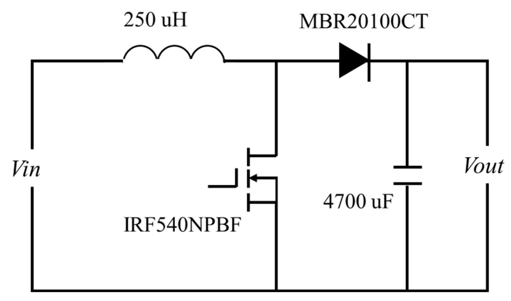
Figure 5.
The circuit diagram of the power converter.
Figure 5.
The circuit diagram of the power converter.
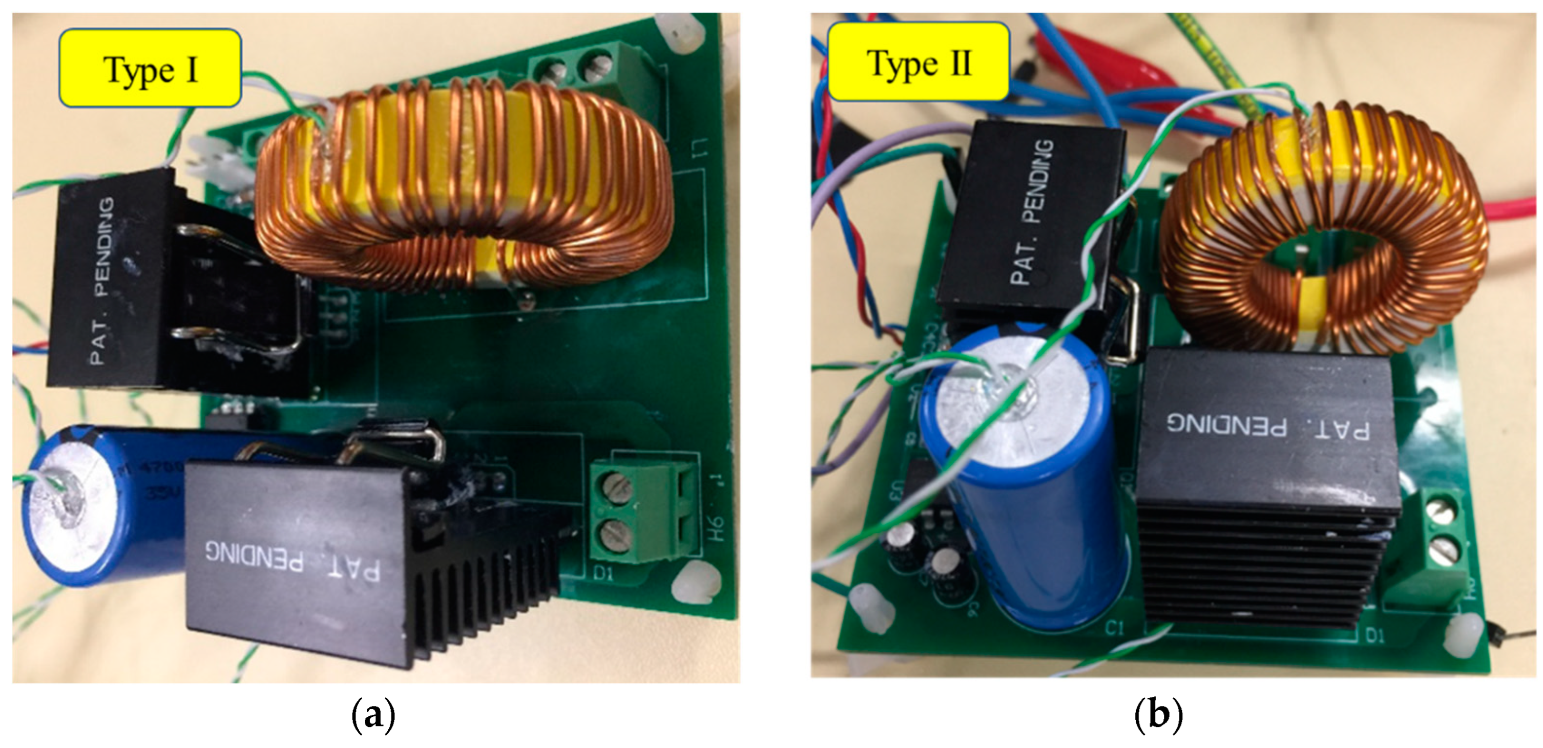
Figure 6.
Two different types of power converters: (a) type I with large device spacing; (b) type II with small device spacing.
Figure 6.
Two different types of power converters: (a) type I with large device spacing; (b) type II with small device spacing.
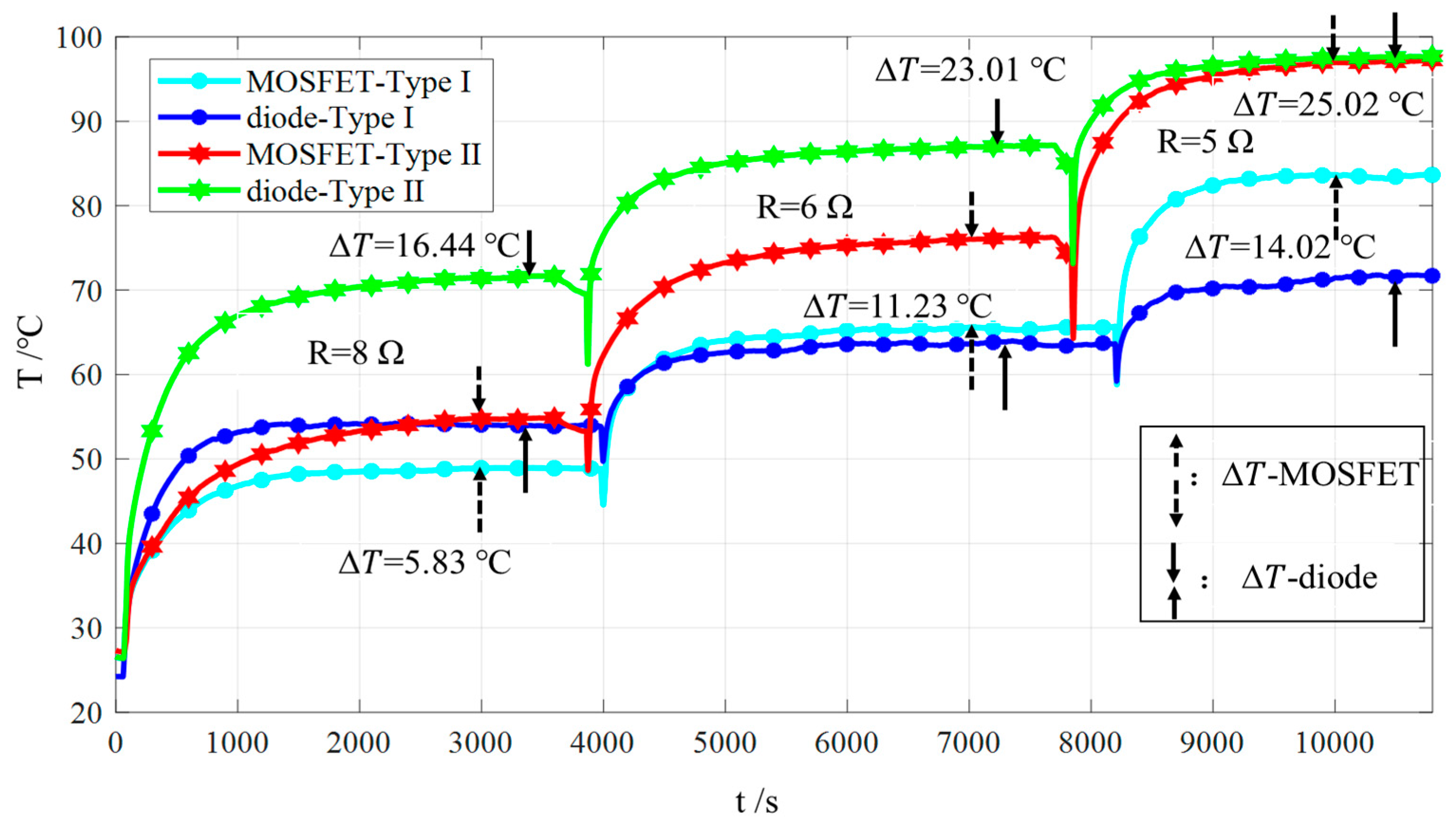
Figure 7.
The comparisons of the case temperatures and the temperature differences of the power devices with different spacing types.
Figure 7.
The comparisons of the case temperatures and the temperature differences of the power devices with different spacing types.
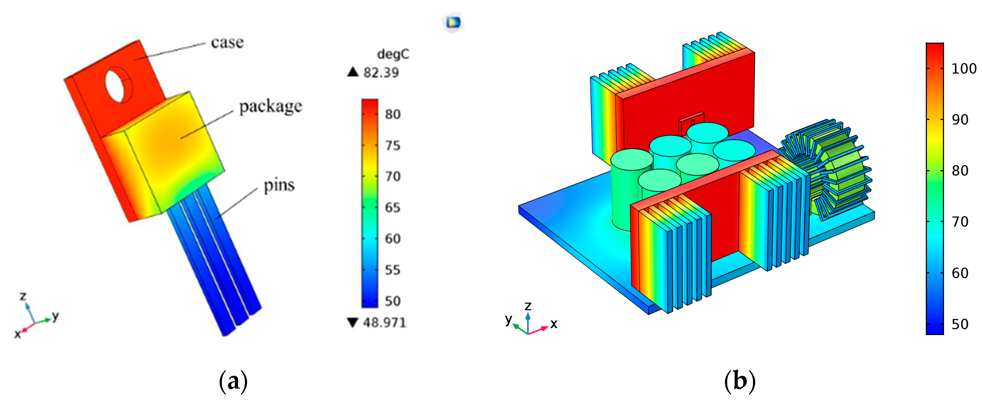
Figure 8.
FEM thermal analysis model: (a) three-dimensional thermal calculation model for a MOSFET; (b) temperature distributions of a power converter.
Figure 8.
FEM thermal analysis model: (a) three-dimensional thermal calculation model for a MOSFET; (b) temperature distributions of a power converter.
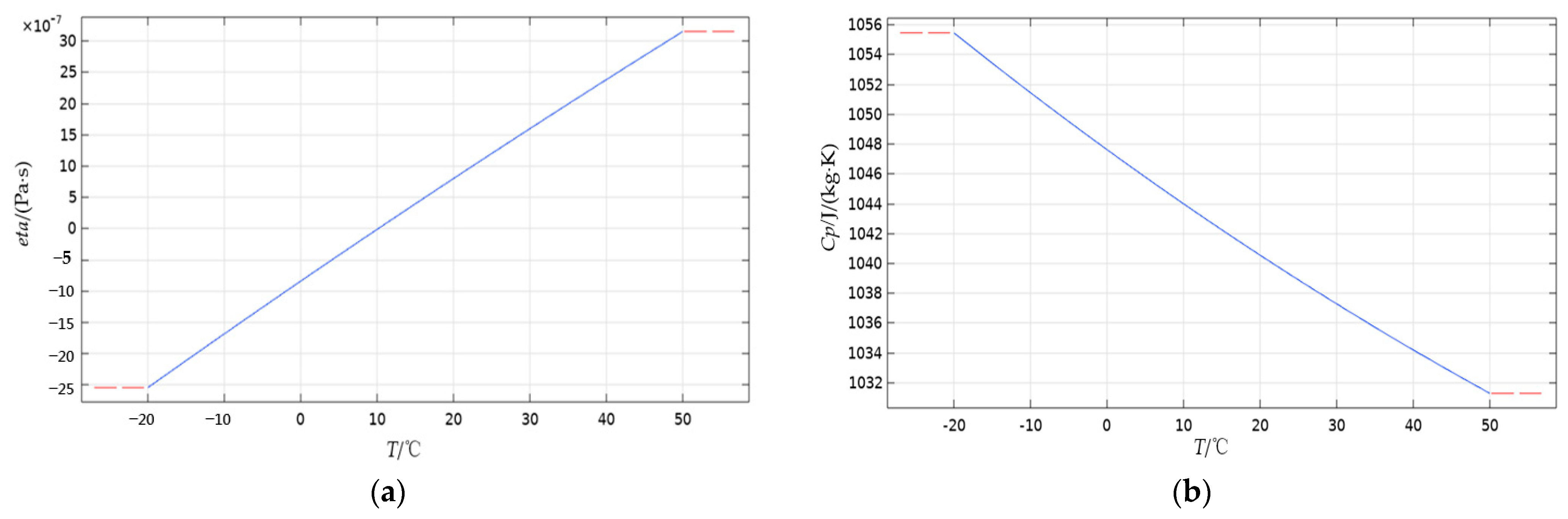
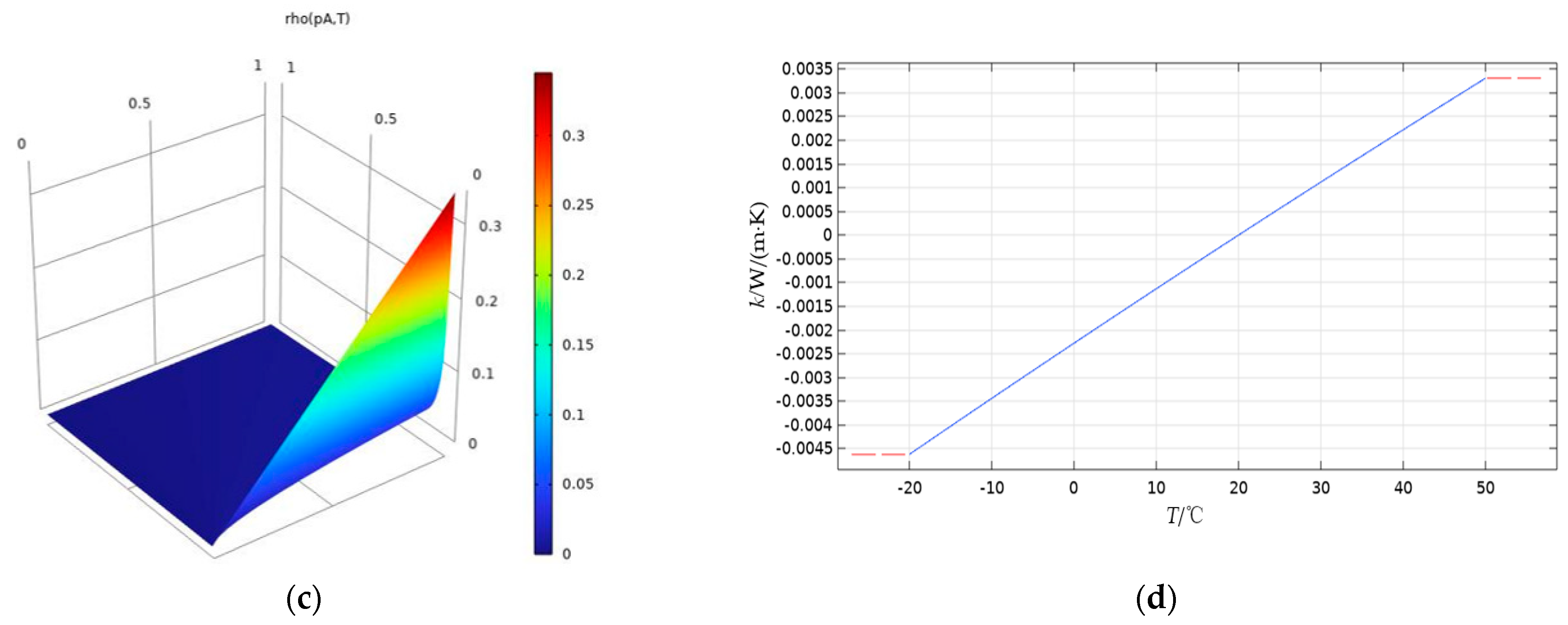
Figure 9.
Ambient domain parameters: (a) kinetic viscosity; (b) constant pressure heat capacity; (c) density; (d) thermal conductivity of air.
Figure 9.
Ambient domain parameters: (a) kinetic viscosity; (b) constant pressure heat capacity; (c) density; (d) thermal conductivity of air.
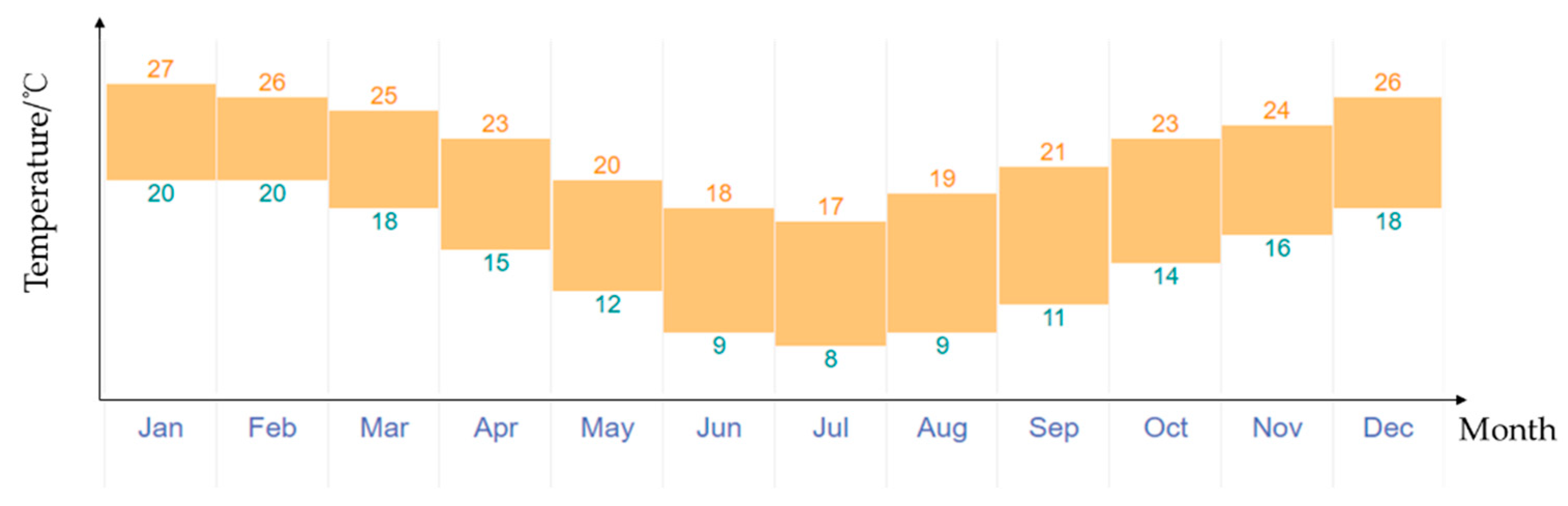
Figure 10.
The all-year climate (annual weather averages) in Sydney.
Figure 10.
The all-year climate (annual weather averages) in Sydney.
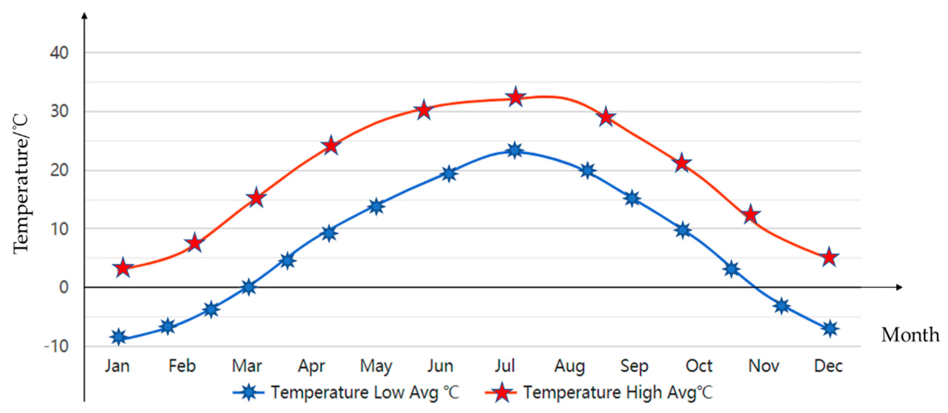
Figure 11.
The temperature change in 2022 in Beijing.
Figure 11.
The temperature change in 2022 in Beijing.
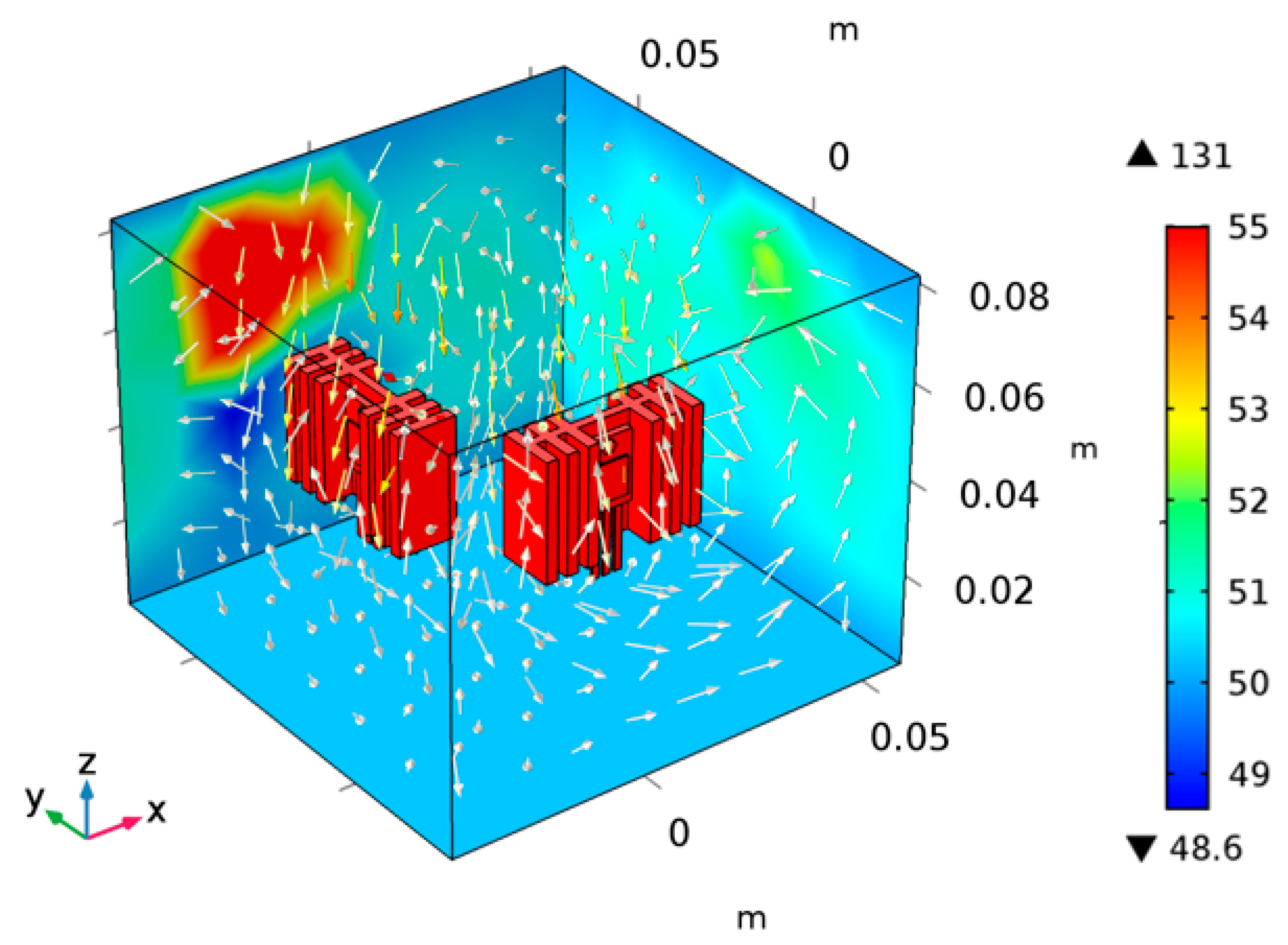
Figure 12.
The temperature distribution of convection thermal coupling.
Figure 12.
The temperature distribution of convection thermal coupling.
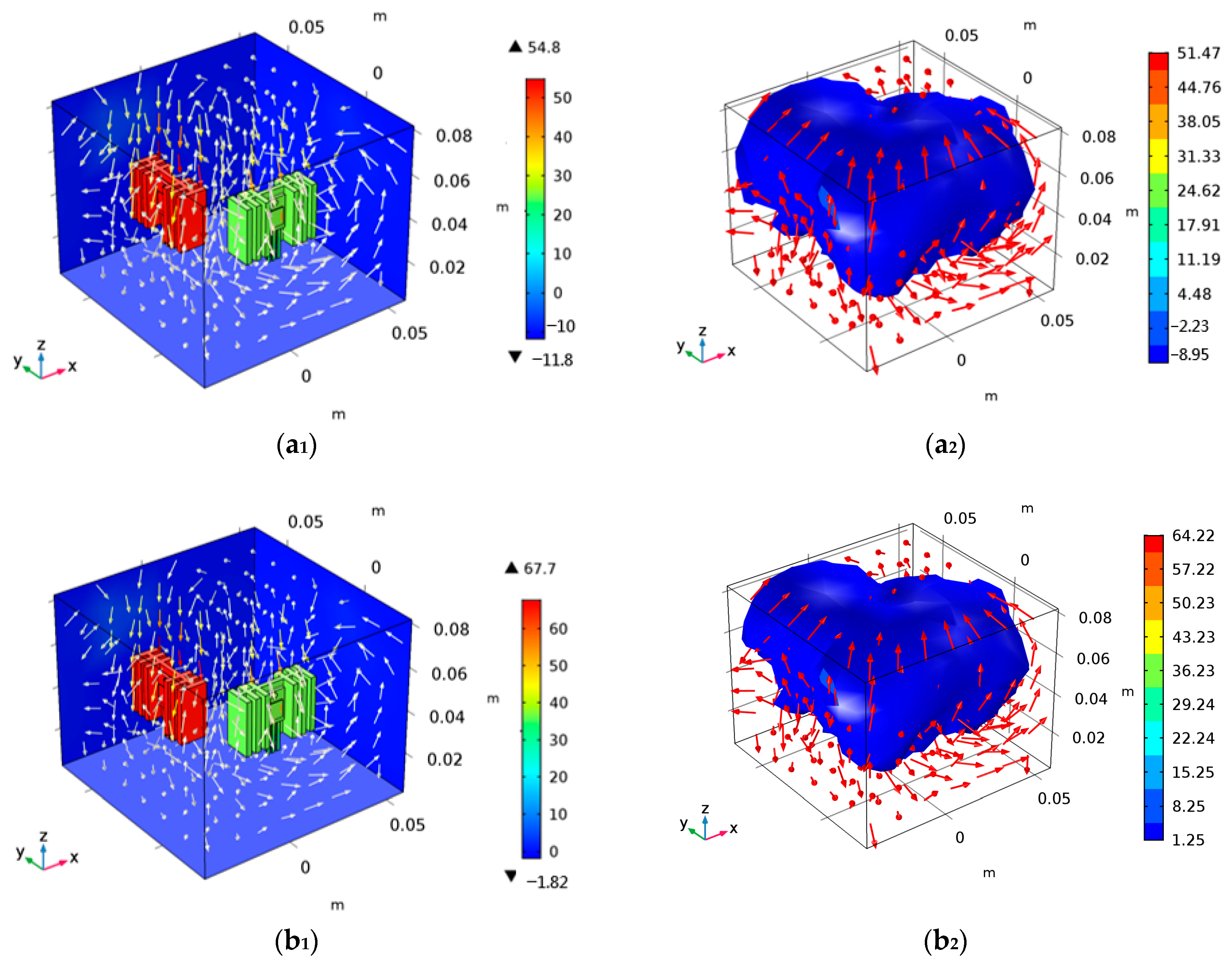
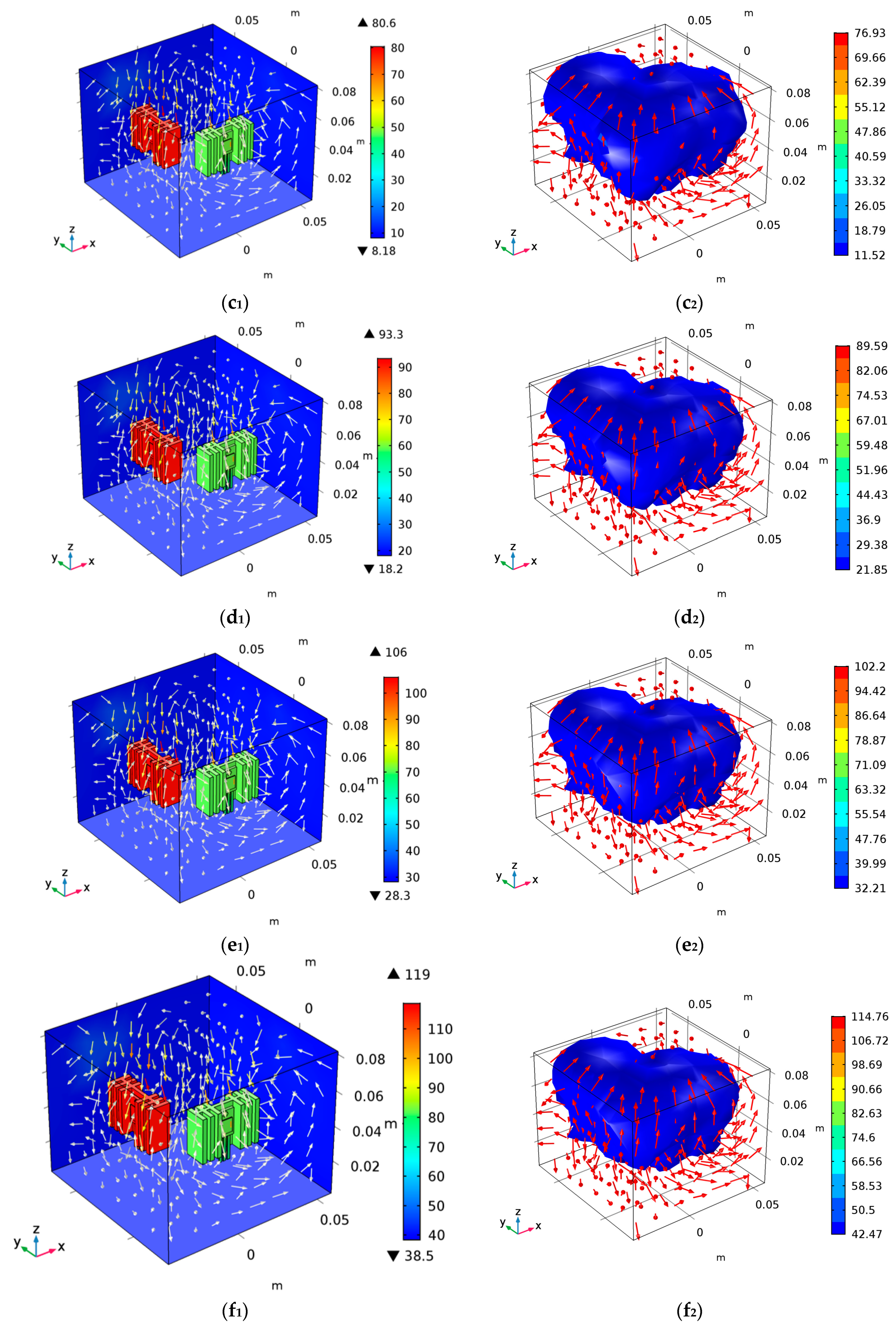
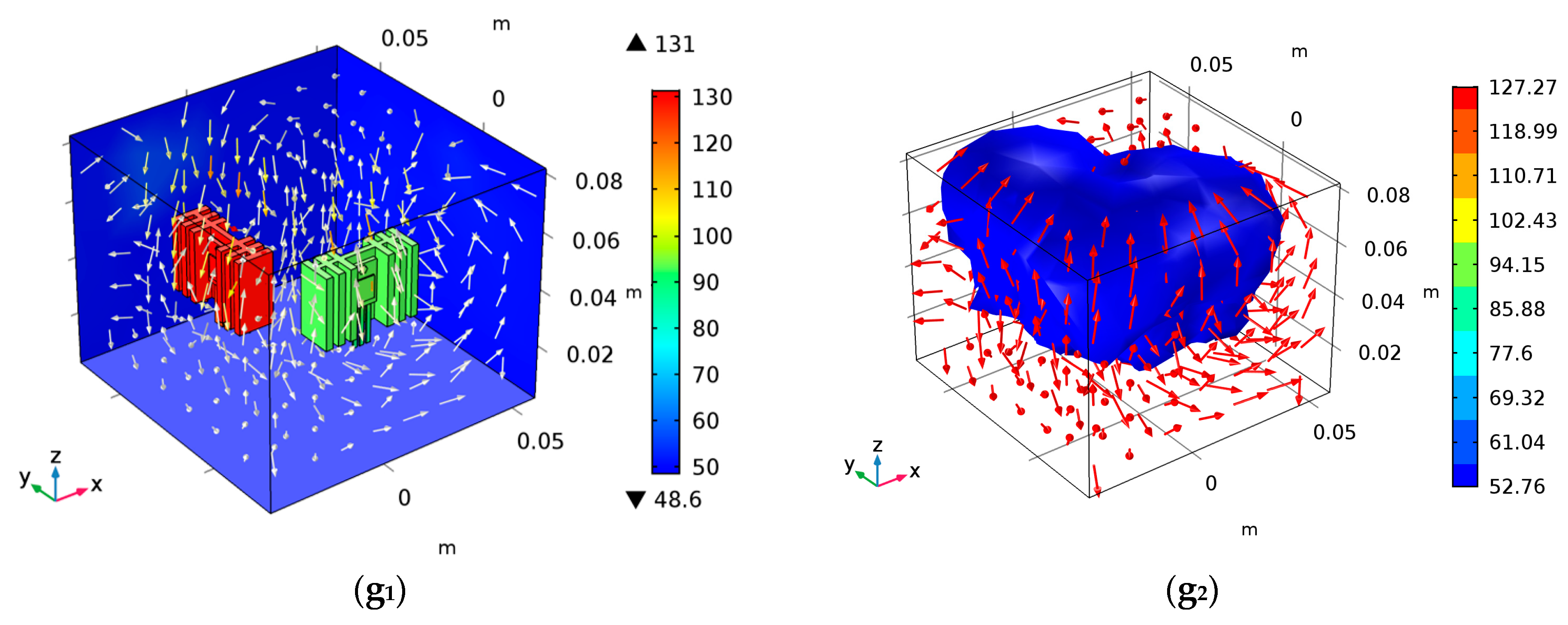
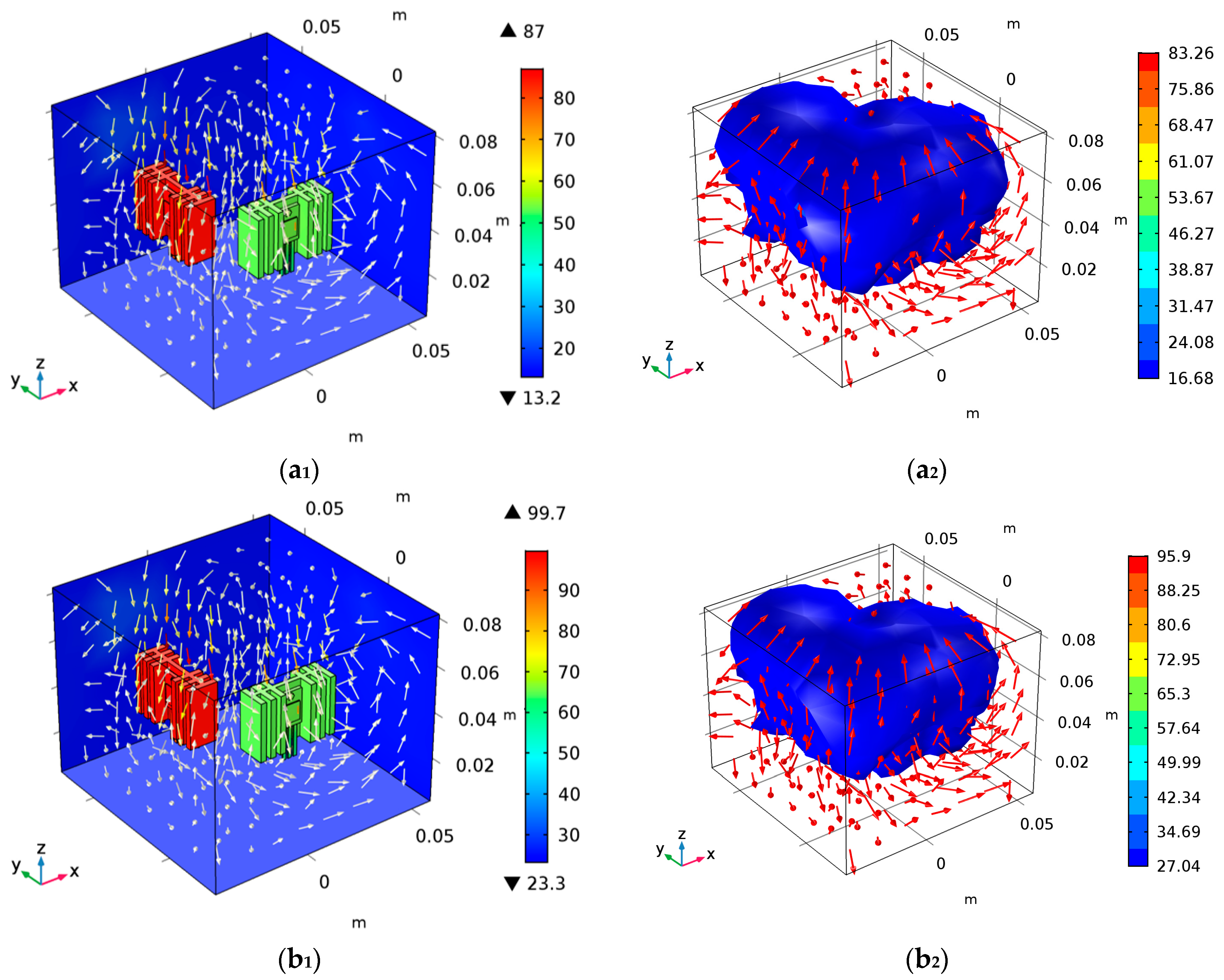
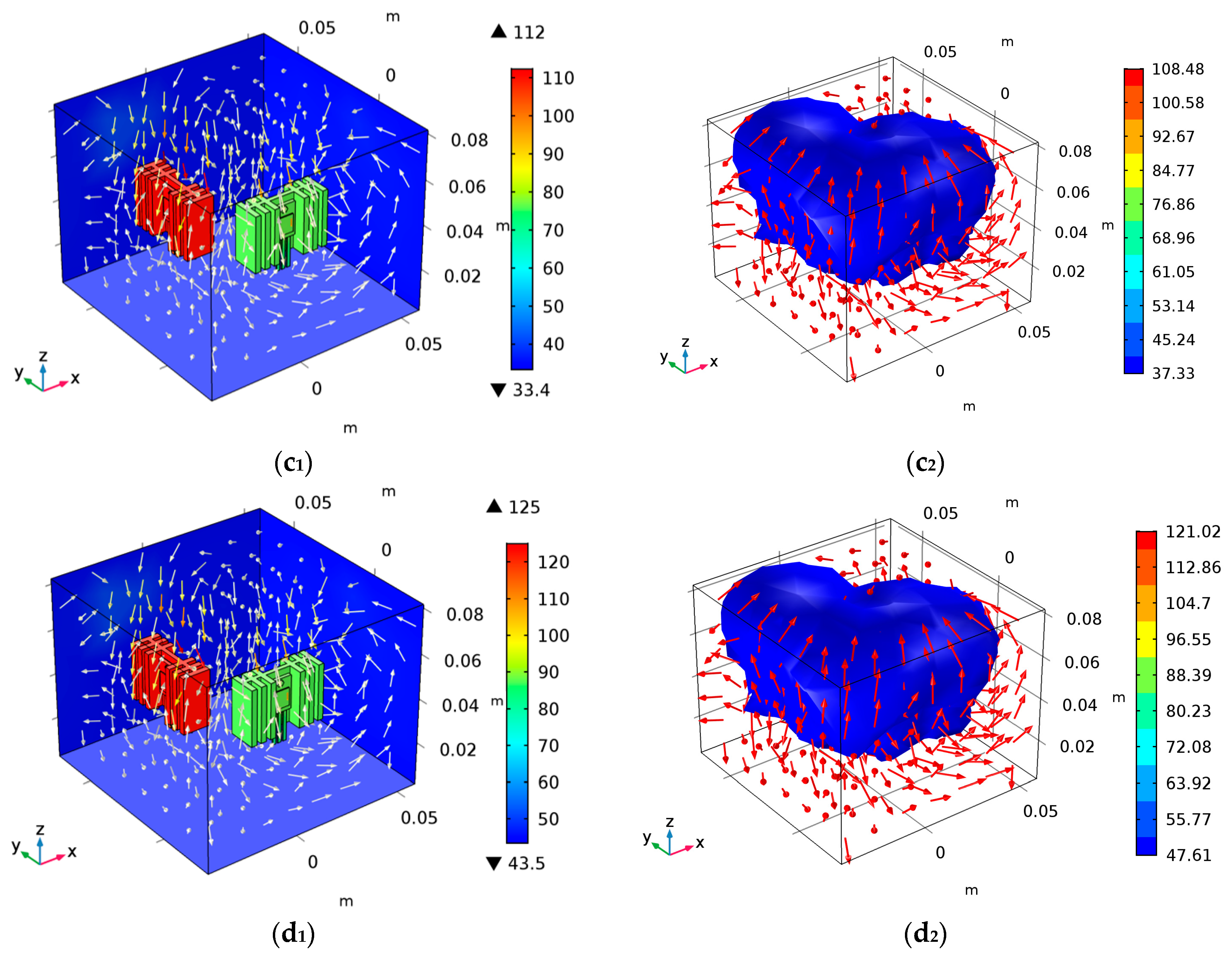
Figure 13.
Simulation analysis of convection thermal coupling. (a1,a2) are temperature distribution and iso-surface distribution when Ta = −10 °C; (b1,b2) are temperature distribution and iso-surface distribution when Ta = 0 °C; (c1,c2) are temperature distribution and iso-surface distribution when Ta = 10 °C; (d1,d2) are temperature distribution and iso-surface distribution at Ta = 20 °C; (e1,e2) are temperature distribution and iso-surface distribution at Ta = 30 °C; (f1,f2) are temperature distribution and iso-surface distribution at Ta = 40 °C; (g1,g2) are temperature distribution and iso-surface distribution at Ta = 50 °C.
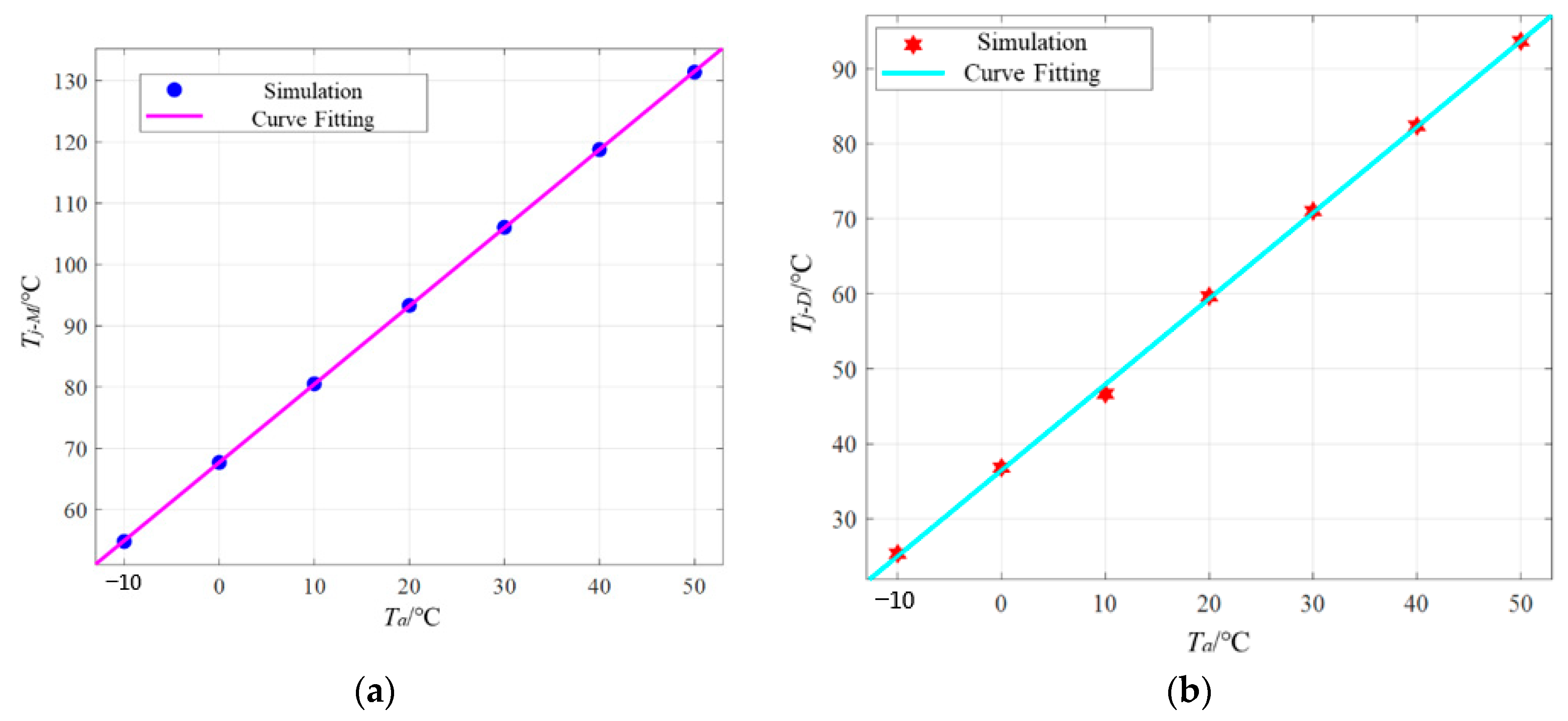
Figure 14.
The relationships between junction and ambient temperatures: (a) for MOSFET, (b) for diode.
Figure 14.
The relationships between junction and ambient temperatures: (a) for MOSFET, (b) for diode.
Figure 15.
The simulation analysis of convective heat coupling: (a1,a2) are the temperature distribution and iso-surface distribution at Ta = 15 °C, (b1,b2) are the temperature distribution and iso-surface distribution at Ta = 25 °C, (c1,c2) are the temperature distribution and iso-surface distribution at Ta = 35 °C, and (d1,d2) are the temperature distribution and iso-surface distribution at Ta = 45 °C.
Table 1.
The temperature differences of case temperature under different load resistances.
Table 1.
The temperature differences of case temperature under different load resistances.
| R/Ω | 8 | 6 | 5 |
|---|
| ΔTc_M/°C | 5.83 | 11.23 | 14.02 |
| ΔTc_D/°C | 16.44 | 23.01 | 25.02 |
Table 2.
Rca for the MOSFET.
Table 2.
Rca for the MOSFET.
| Tc_M [°C] | Rca_M [°C/W] |
|---|
| 25.75 | 69.32 |
| 34.43 | 62.73 |
| 53.27 | 61.76 |
| 80.01 | 54.27 |
| 146.85 | 45.15 |
Table 3.
Rca for the diode.
Table 3.
Rca for the diode.
| Tc_D [°C] | Rca_D [°C/W] |
|---|
| 50.66 | 60.39 |
| 79.59 | 58.89 |
| 105.85 | 54.35 |
| 129.26 | 52.24 |
| 149.19 | 49.60 |
Table 4.
Ambient domain parameters.
Table 4.
Ambient domain parameters.
| Name | Symbol | Unit |
|---|
| kinetic viscosity | eta (T) | Pa·s |
| constant pressure heat capacity | Cp (T) | J/(kg·K) |
| density | ρ (pA,T) | kg/m3 |
| thermal conductivity | k (T) | W/(m·K) |
Table 5.
The junction temperatures at different ambient temperatures.
Table 5.
The junction temperatures at different ambient temperatures.
| Ta/°C | −10 | 0 | 10 | 20 | 30 | 40 | 50 |
|---|
| Tj_M/°C | 54.81 | 67.70 | 80.54 | 93.33 | 106.07 | 118.76 | 131.40 |
| Tj_D/°C | 25.35 | 36.82 | 46.65 | 59.66 | 71.03 | 82.37 | 93.67 |
Table 6.
The junction temperature comparisons of the calculation and simulation for the MOSFET.
Table 6.
The junction temperature comparisons of the calculation and simulation for the MOSFET.
| Ta/°C | 15 | 25 | 35 | 45 |
|---|
| Tc_M/°C (Calculation) | 86.87 | 99.63 | 112.39 | 125.15 |
| Tc_M/°C (FEM) | 86.94 | 99.71 | 112.42 | 125.08 |
| Error/% | 0.08 | 0.08 | 0.03 | 0.06 |
Table 7.
The junction temperature comparisons of the calculation and simulation for the diode.
Table 7.
The junction temperature comparisons of the calculation and simulation for the diode.
| Ta/°C | 15 | 25 | 35 | 45 |
|---|
| Tc_D/°C (Calculation) | 53.58 | 64.98 | 76.38 | 87.78 |
| Tc_D/°C (FEM) | 53.96 | 65.35 | 76.70 | 88.02 |
| Error/% | 0.70 | 0.57 | 0.42 | 0.27 |


