Communication

Process Development of Low-Loss LPCVD Silicon Nitride Waveguides on 8-Inch Wafer

1
School of Microelectronics, Shanghai University, Shanghai 201800, China
2
Shanghai Institute of Microsystem and Information Technology (SIMIT), Chinese Academy of Sciences (CAS), Shanghai 200050, China
3
Shanghai Industrial μTechnology Research Institute, Shanghai 201800, China
*
Authors to whom correspondence should be addressed.
Appl. Sci. 2023, 13(6), 3660; https://doi.org/10.3390/app13063660
Submission received: 22 February 2023 / Revised: 10 March 2023 / Accepted: 12 March 2023 / Published: 13 March 2023
(This article belongs to the Special Issue Laser and Silicon Photonics: Technology, Preparation and Application)

Abstract

:
Silicon nitride is a material compatible with CMOS processes and offers several advantages, such as a wide transparent window, a large forbidden band gap, negligible two-photon absorption, excellent nonlinear properties, and a smaller thermo-optic coefficient than silicon. Therefore, it has received significant attention in the field of silicon photonics in recent years. The preparation of silicon nitride waveguides using low-pressure chemical vapor deposition methods results in lower loss and better process repeatability. However, due to the higher temperature of the process, when the thickness of the silicon nitride film exceeds 300 nm on an 8-inch wafer, it is prone to cracking due to the high stress generated by the film. Limited by this high stress, silicon nitride waveguide devices are typically developed on wafers with a thickness of 4 inches or less. In this work, we successfully fabricated a 400 nm-thick silicon nitride waveguide on an 8-inch wafer using a Damascene method similar to the CMOS process for copper interconnects and demonstrated propagation losses of only 0.157 dB/cm at 1550 nm and 0.06 dB/cm at 1580 nm.

1. Introduction

Photonic integration based on Silicon-On-Insulator (SOI) has grown rapidly over the last decade. The main advantages of silicon photonics are the compatibility with complementary metal-oxide-semiconductor (CMOS) infrastructure and the ability to realize monolithic integration. These features enable the fabrication of highly integrated photonic devices in large quantities at low cost. Silicon photonics are theoretically ideal for large-scale complex integrated optical circuits, such as multi-wavelength coherent transceivers, optical interconnection networks, and optical switching networks. However, the narrow silicon bandgap (1.14 eV) and non-negligible multiphoton absorption effects in the near and partial mid-infrared bands increase transmission losses and limit the application field of silicon waveguides [1,2]. In contrast, silicon nitride (Si3N4) is also a CMOS-compatible material with a moderate refractive index between silicon dioxide (SiO2) and silicon (Si), a large energy band gap (5.0 eV), and a wide transparent optical window (0.25–8.0 μm), which covers the visible to mid-infrared band [3,4]. This means that intrinsic silicon nitride material has low absorption properties and can achieve low loss in broadband. Its advantages are also manifested in the following aspects: 1. A lower thermo-optic coefficient: it is one order of magnitude smaller than that of silicon, so that silicon nitride optical components are much less sensitive to temperature than silicon optical components. This makes them more suitable for applications that need to avoid the influence of temperature and have better popularity. 2. Negligible two-photon absorption: two-photon absorption limits the power handling capacity of the silicon waveguide in the near-infrared band; while benefitting from the negligible two-photon absorption, the silicon nitride waveguide can sustain much higher optical power, which makes it a more suitable material for nonlinear optics compared to silicon even with a lower nonlinear index. 3. A wide range of application scenarios, including artificial intelligence, lasers, optical communication, biomedicine, optical sensors, optical distance measurement, etc. [1,5,6,7,8,9].
For silicon nitride, there are two common deposition methods: plasma-enhanced chemical vapor deposition (PECVD) and low-pressure chemical vapor deposition (LPCVD). Although PECVD can achieve a thick silicon nitride film, the uniformity is poor compared to that of LPCVD. Furthermore, the film deposited by PECVD is not stoichiometric and contains more H-bonds (about 20%), which will generate a large absorption in the communication band and seriously affect the device loss due to the N-H and Si-H bonds [10,11]. Compared with PECVD, the silicon nitride film deposited by LPCVD has a more uniform thickness and lower H-bond content. However, due to the difference in the thermal expansion coefficient between silicon nitride and substrate silicon (the thermal expansion coefficient of silicon nitride is: 2.35 × 10⁻⁶/°C, which is smaller than 2.61 × 10⁻⁶/°C of silicon) [11,12,13,14,15,16,17], the film deposited by LPCVD has larger stress due to higher process temperature, and the stress will increase with the wafer size. Typically, in an 8-inch wafer, only up to 300 nm-thick silicon nitride films can be deposited; otherwise, cracks will occur. Due to the high stress, thick LPCVD silicon nitride waveguide devices are typically developed on a 4-inch wafer and require a two-step deposition method. These factors limit low-loss silicon nitride waveguides from achieving higher levels of integration and higher economic value [2,4,18,19,20].
Although there are some reports on low-loss waveguides in recent years, such as adjusting the precursor gas of the PECVD process [2], the report used N2 instead of NH3 to reduce the H-bond content of the silicon nitride film deposited by PECVD. The loss of the final silicon nitride waveguide is 2.1 dB/cm @1550 nm. This is still much higher than that of the silicon nitride waveguide prepared by LPCVD of the same size. Secondly, there are also reports that in order to reduce the stress of the silicon nitride film deposited by LPCVD [21], the gas ratio of SiH2Cl2 and NH3 was adjusted so that the deposited film was a silicon nitride film rich in silicon. Although this method reduced the stress of the silicon nitride film, it also changed the material properties of the silicon nitride film, making it closer to silicon material, which led to the loss of some advantages of the standard stoichiometric ratio silicon nitride film. The loss of the final silicon nitride waveguide was 1.5 dB/cm @1550 nm. In addition, some new special structures of silicon nitride waveguides have also been reported [22,23]; although these waveguides have low loss, the limiting capability of the optical field is weak, the critical bending radius is generally large (≥500 μm) for integration, and the process is complex. Recently, an interesting idea was proposed: to increase the confinement ability of the waveguide to the light field by integrating it with other materials [24,25]. Still, because of our current conditions, some related explorations can be carried out in the future. Therefore, the preparation of low-loss and high-limiting-capacity silicon nitride waveguides still starts from the direction of how to prepare thick standard stoichiometric ratio silicon nitride waveguides via the LPCVD process.
In order to solve the above problem, we proposed a method and successfully fabricated silicon nitride waveguides with a thickness of 400 nm by LPCVD on an 8-inch wafer in accordance with standard stoichiometric ratios. The silicon nitride waveguides prepared via this process showed significant advantages of low propagation loss and small critical bending radius. The measurement results show that the propagation loss is only 0.157 dB/cm at 1550 nm and 0.06 dB/cm at 1580 nm; for a bending waveguide with a bending radius of 50 µm, the bending loss is only 0.013 dB, and for a bending radius of 80 µm, the bending loss is only 0.0095 dB. This greatly improves the integration of the optical chip and achieves higher economic value.

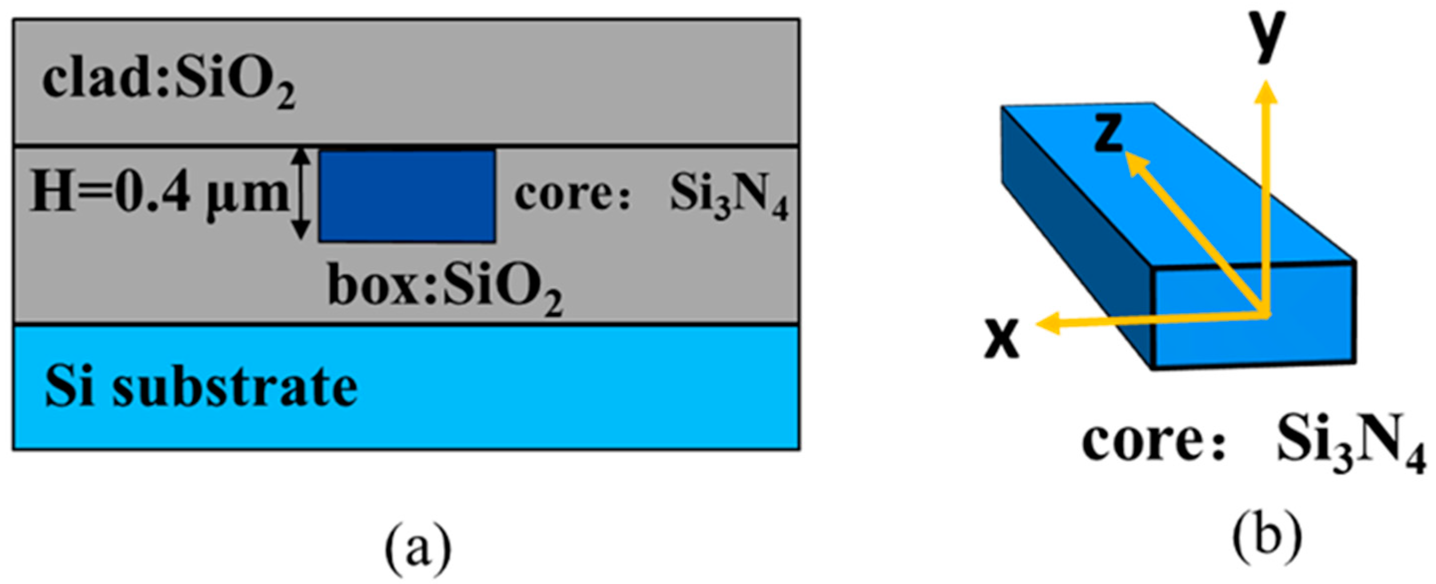
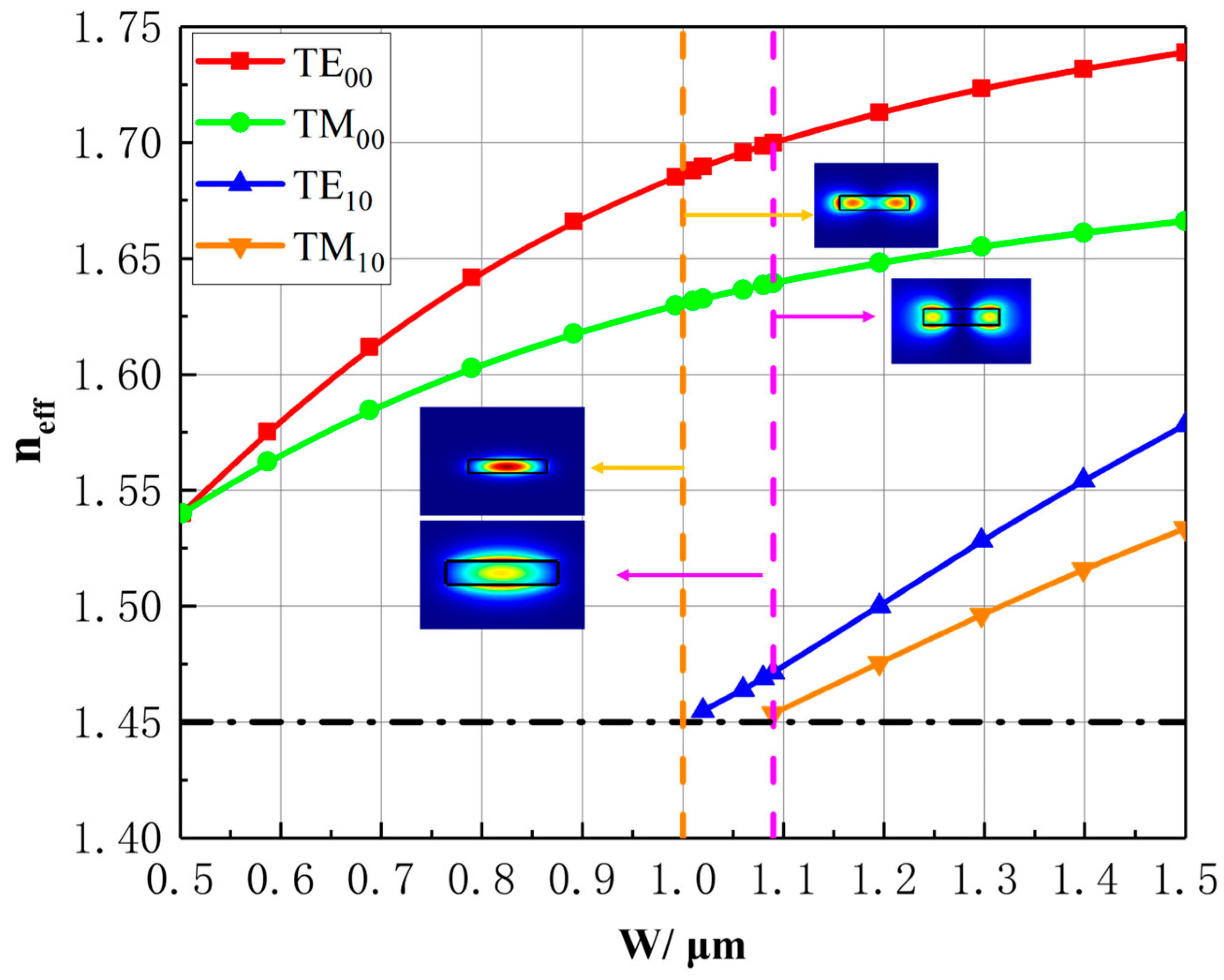
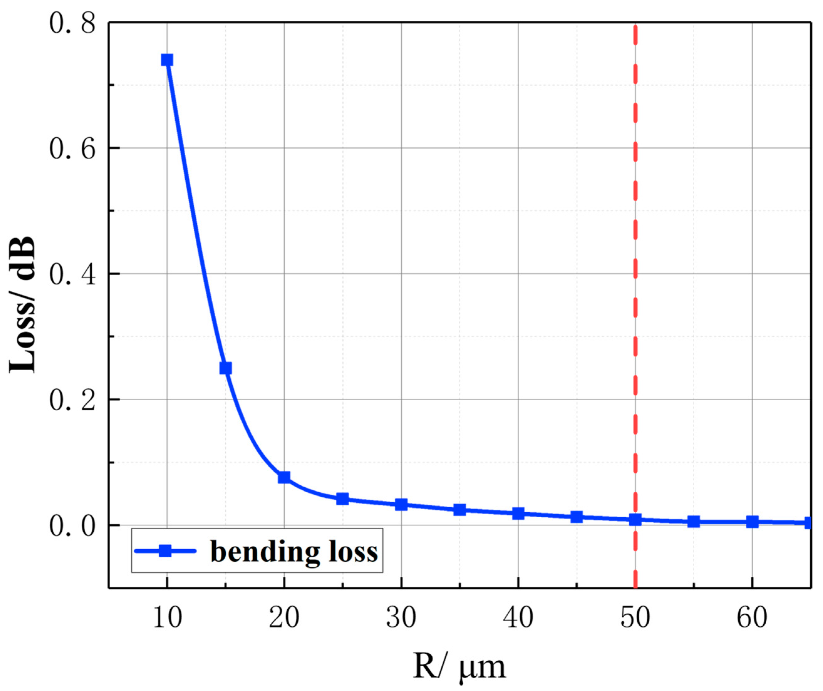
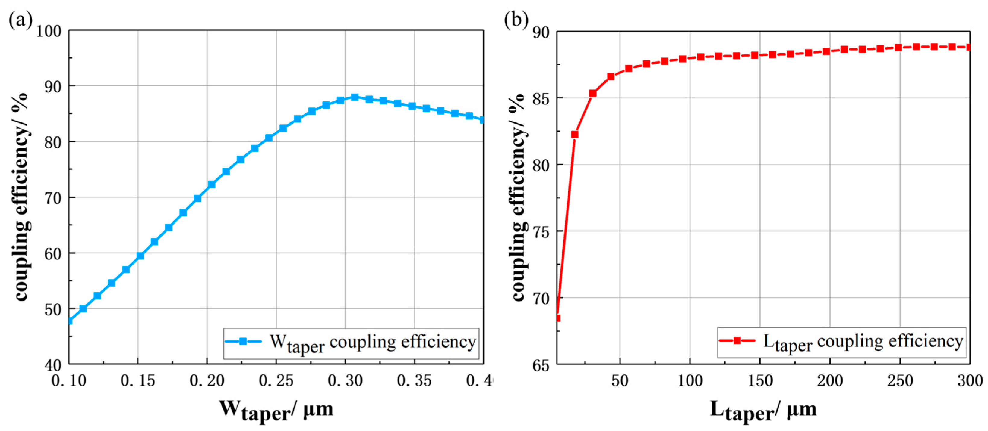
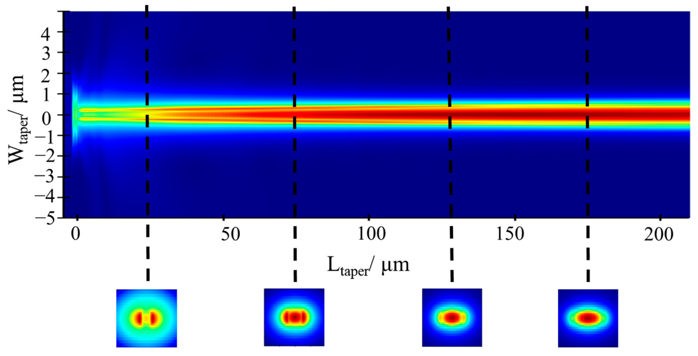
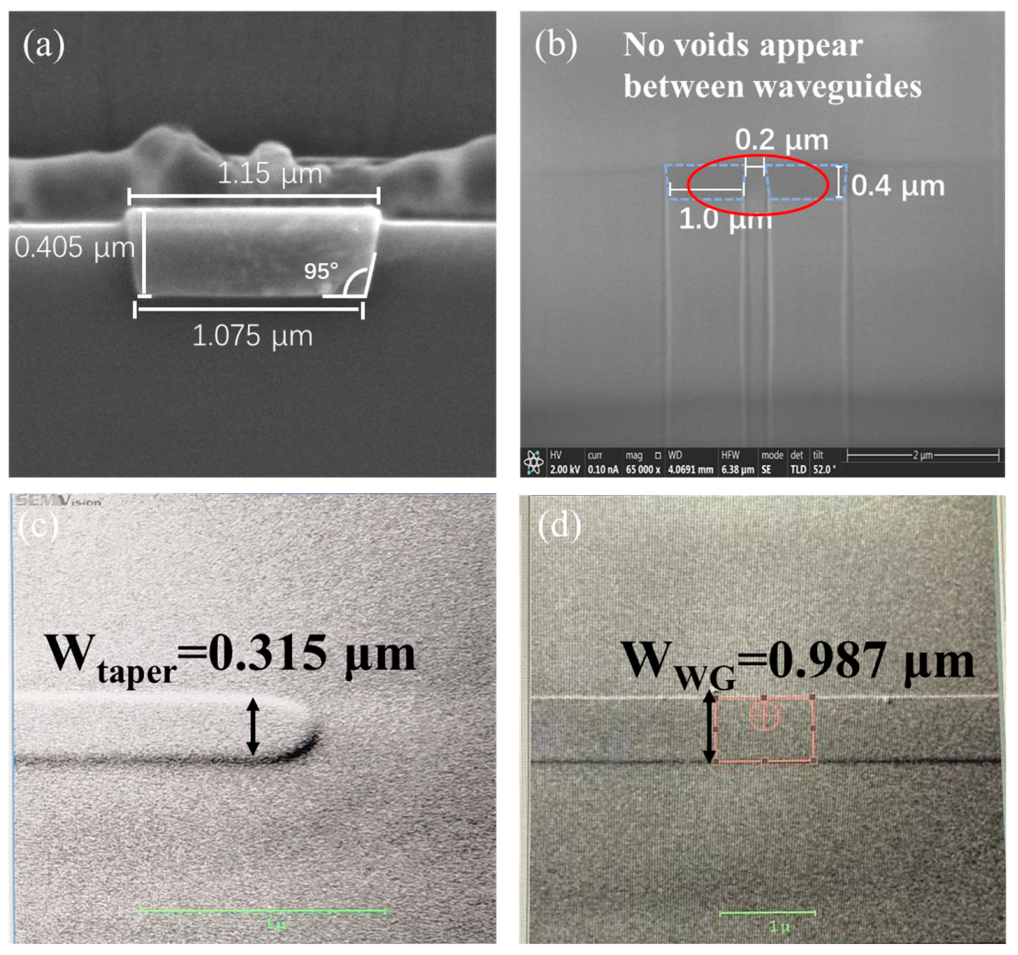
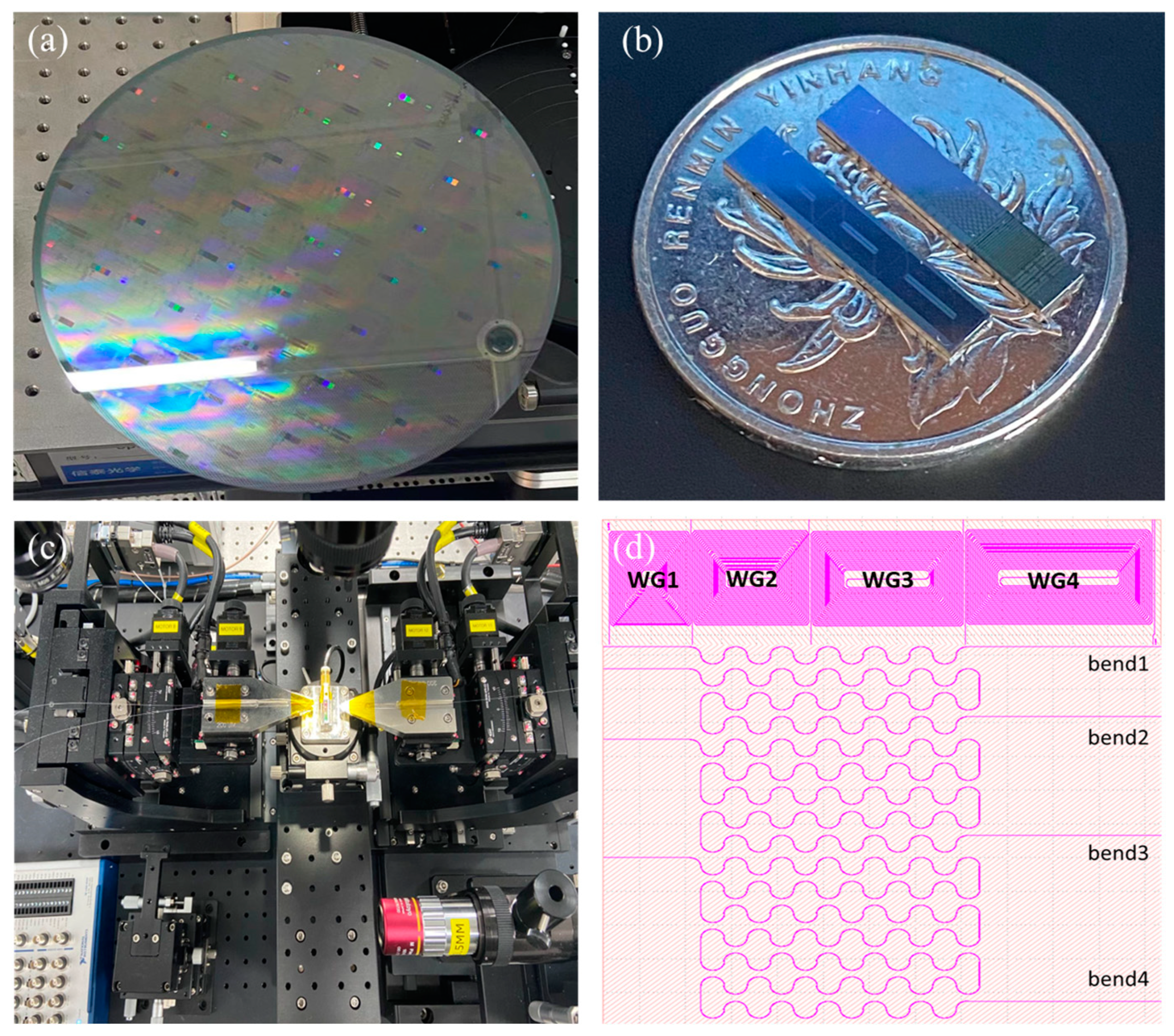
2. Design of Silicon Nitride Waveguide

In silicon photonic integrated circuits, a rectangular optical waveguide is the basic component, and a single-mode waveguide is commonly used to avoid inter-mode interference and mode dispersion. In order to guarantee the single-mode condition of the Si3N4 rectangular waveguide, we have simulated the mode properties of the Si3N4 waveguide using the Finite Difference Eigenmode solver (FDE) in Lumerical’s Mode Solution software. The structure is shown in Figure 1a; the thickness of the lower cladding layer is 3.6 μm, the thickness of the core layer is 0.4 μm, and the thickness of the upper cladding layer is 2.6 μm.
To determine the single mode condition, the width of the silicon nitride waveguide was scanned at a wavelength of 1550 nm, and the relationship between the waveguide width and the effective refractive index (neff) of the waveguide is shown in Figure 2. According to the orange dashed line, the width limit of the single-mode condition is 1.0 μm.
Based on the above simulation, the critical bending radius of the waveguide with a width of 1.0 μm was then simulated by the FDTD (Finite Difference Time Domain) simulation module. The relationship between the bending loss and the bending radius is shown in Figure 3. With the increasing bending radius, the bending loss decreases exponentially. When the bending radius is larger than 50 μm, the bending loss of pre 90° bending waveguide basically remains smaller than 0.0092 dB, so we set the minimum bending radius to 50 μm in the optical circuits.
In order to test the waveguide, an edge coupler was used for the coupling between the waveguide and the fiber in this work, considering the higher coupling efficiency, polarization independency, and wider bandwidth compared to the grating coupler [26,27,28]. The structure of the edge coupler is shown in Figure 3. In order to avoid damaging the coupler during the deep trench process, the coupler tip is set 2 μm away from the deep trench.
Based on the structure shown in Figure 4, we set the mode field diameter (MFD) of the light source to 2.5 μm, similar to that of the lensed fiber we used in tests; the effect of the tip width (Wtaper) was firstly simulated with the length (Ltaper) of 100 μm. The Wtaper was scanned from 0.1 μm to 0.4 μm, and the results are shown in Figure 5a. The highest coupling efficiency of 88.1% was achieved at Wtaper = 0.3 μm, so we set the Wtaper to 0.3 μm in our design. Subsequently, the Ltaper was simulated with a Wtaper of 0.3 μm. The Ltaper was scanned from 5 μm to 300 μm; the results are shown in Figure 5b. In the range of 5–50 μm, the condition of adiabatic coupling could not be achieved, which caused large radiation loss. The coupling efficiency was stable after 100 μm, and a coupling efficiency of 88.6% was realized with a length of 200 μm.
The final structural parameters of the inverse tapered edge coupler are shown in Table 1. The simulation results are shown in Figure 6. It can be seen that the lightwave is transferred to the well-confined waveguide from the input fiber through the edge coupler.

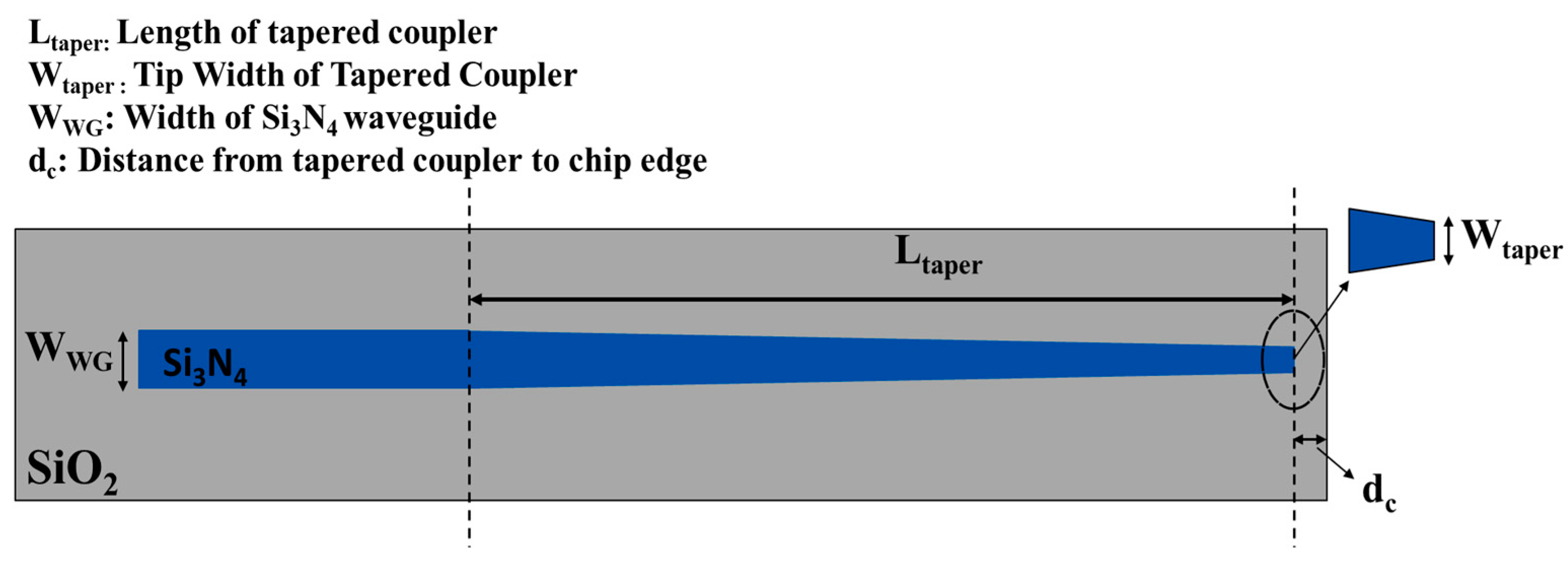
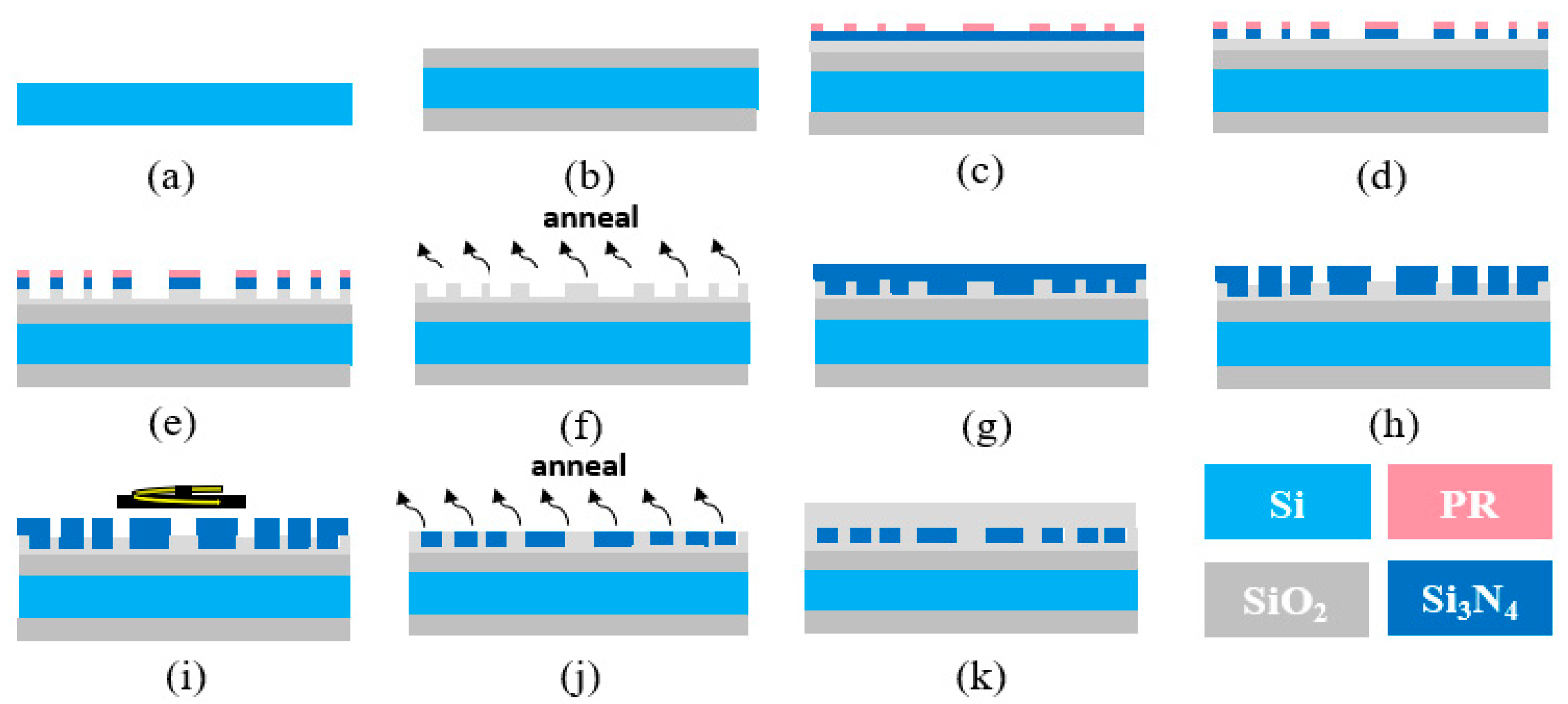
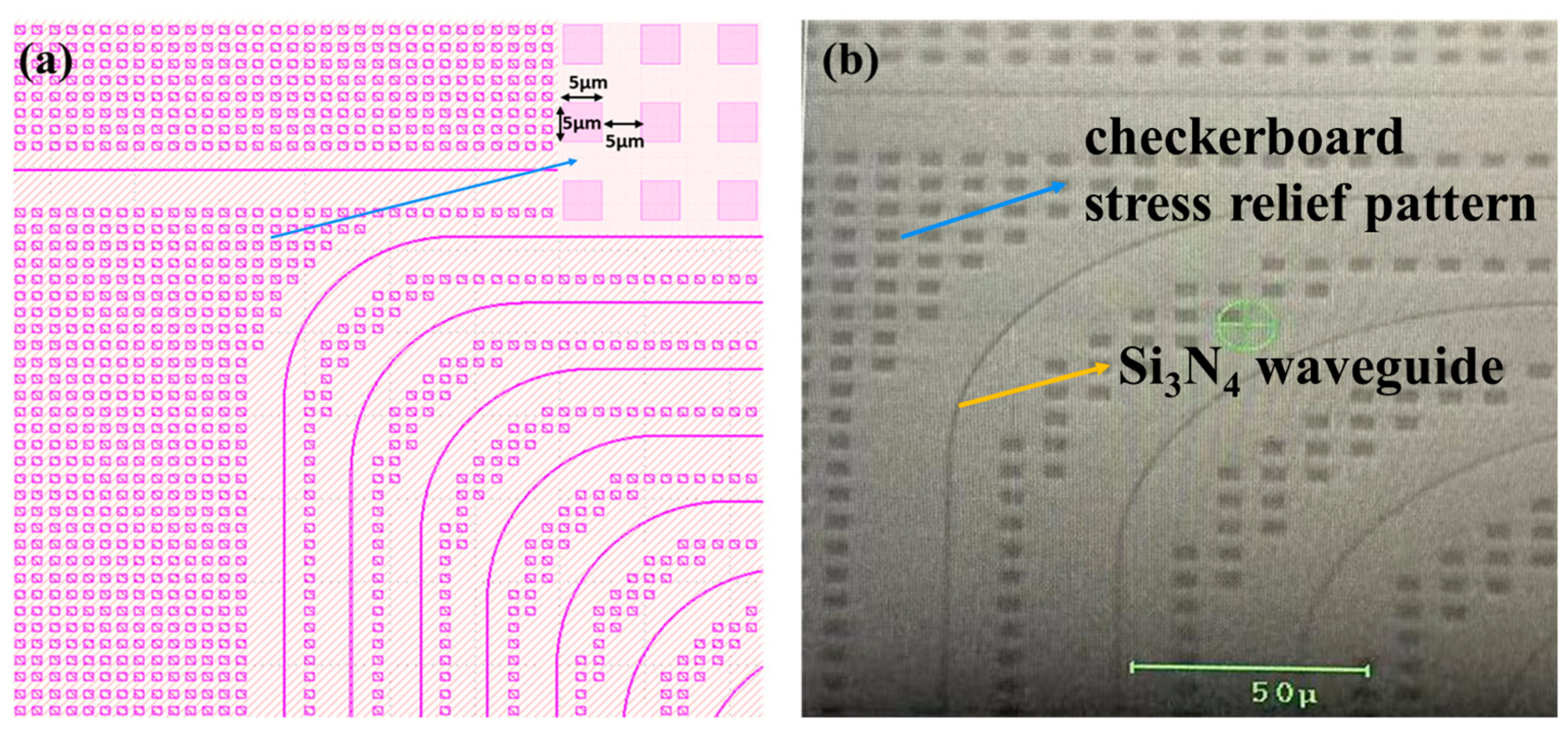
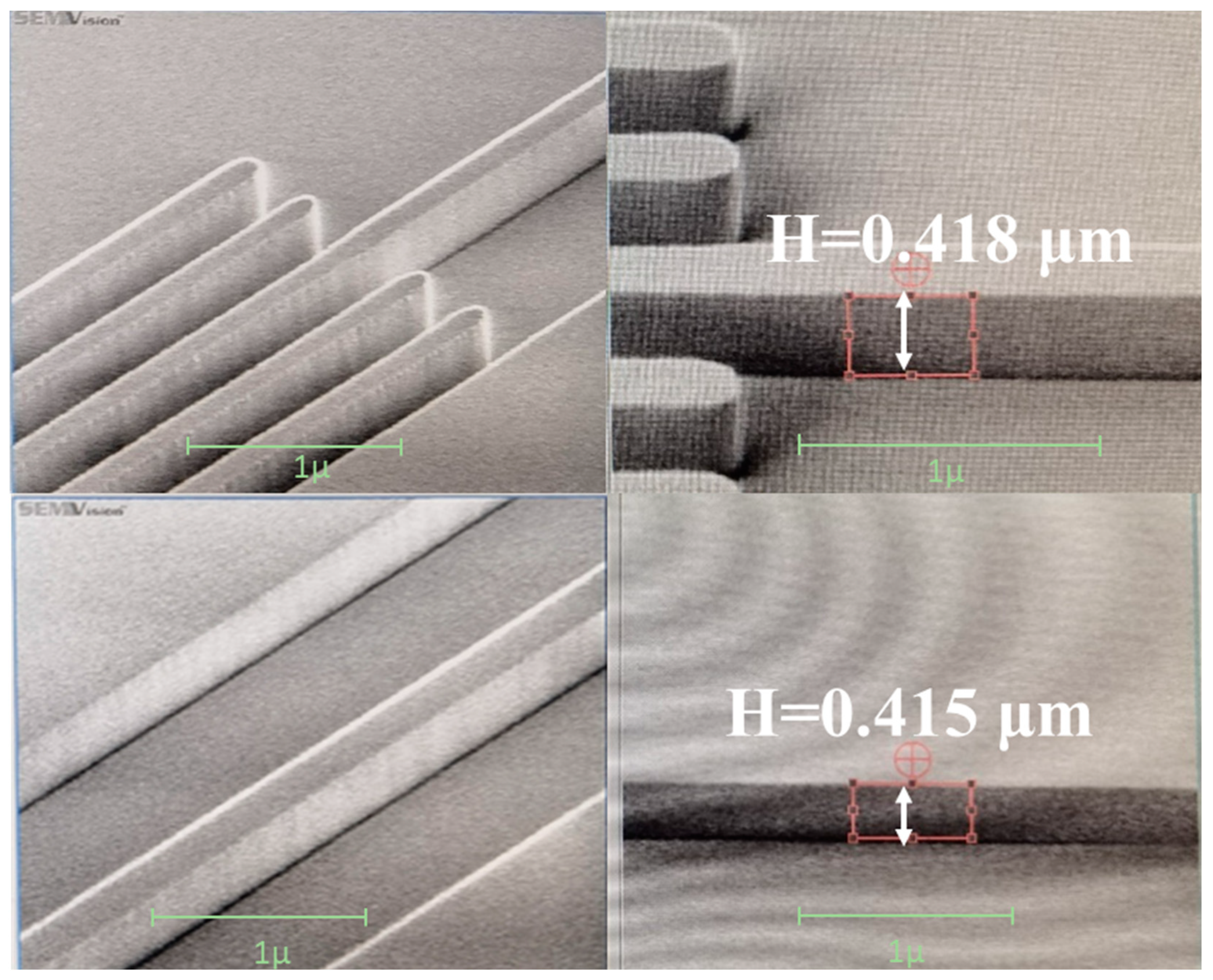
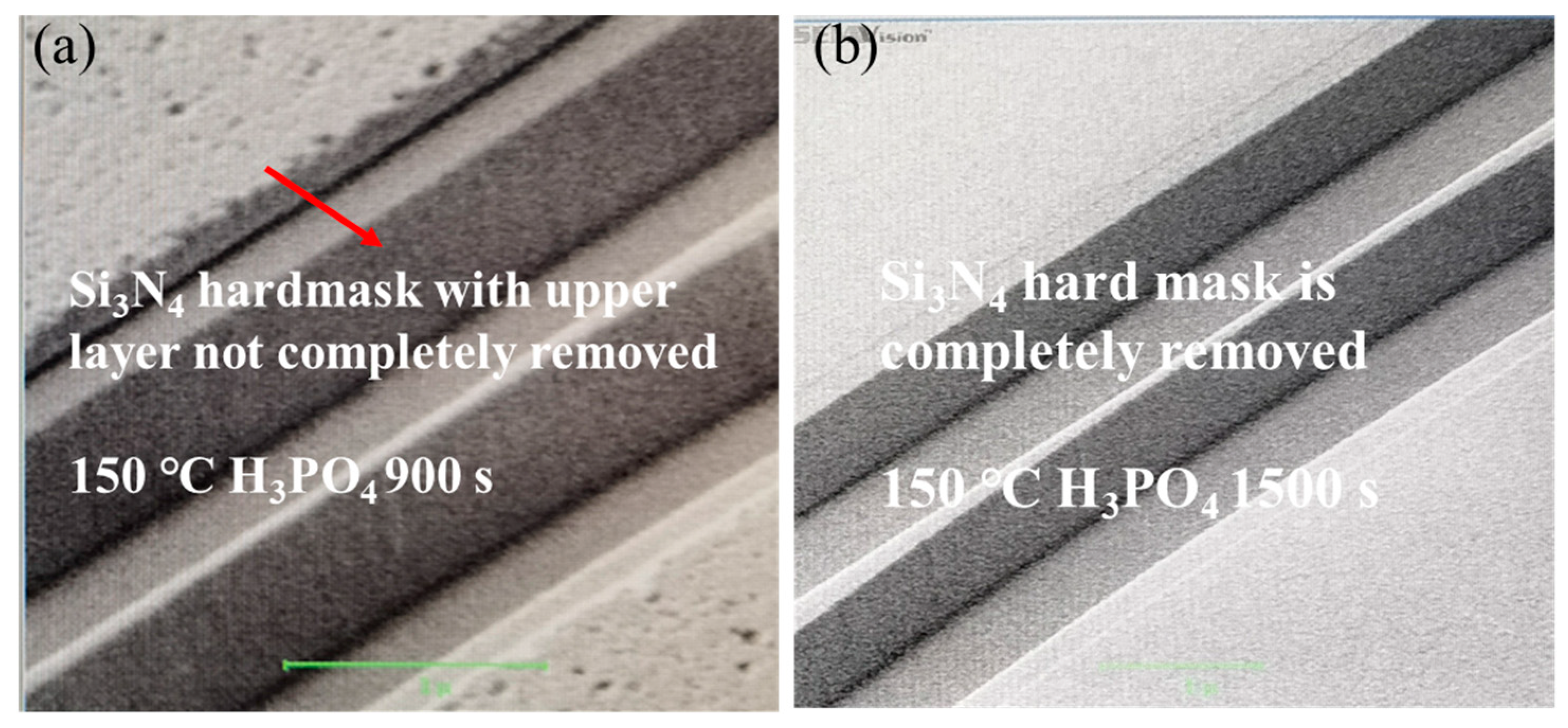
3. Fabrication Process

The suggested fabrication process flow of the Si3N4 waveguide on an 8-inch CMOS line is shown in Figure 7.
Firstly, the BOX layer was split into two steps: 3 μm thermal SiO2 and 1 μm PECVD SiO2. A 3 μm-thick SiO2 was grown on an 8-inch bare silicon wafer using a thermal oxide process. The oxide was grown on both sides of the wafer in this process, which limited the deformation of the wafer due to stress. Following this was the deposition of 1 μm SiO2 via the PECVD process. We separated the BOX layer into two steps due to two considerations: 1. The texture of the SiO2 film deposited by the PECVD process was looser, and thus easier to etch and reflow in the following annealing process. 2. The processing time of thermal oxide increases drastically with the increase in thickness; reducing 1 μm can save much time in the thermal oxide process. In addition, the loose PECVD SiO2 would harden in the following annealing process to form the property close to thermal oxide. Secondly, a layer of PECVD Si3N4 film was deposited as the hard mask (HM) layer in the etching of the waveguide layer. Then the waveguide layer was patterned and etched on the BOX layer with a depth of around 0.42 μm, which balanced the loss of the BOX layer in the following chemical mechanical polishing (CMP) step. At the same time, in order to limit the stress of the silicon nitride film on the wafer, as shown in Figure 8, we added a checkerboard stress relief pattern that could make the film into a discontinuous state on the nonwaveguide position on the wafer. Because phosphoric acid (H3PO4) has a very high selectivity ratio for silicon nitride and silicon oxide, we immersed the wafer in phosphoric acid at 150 °C for 1500 s to completely remove the Si3N4 hard mask while ensuring that it did not damage the BOX layer [29]. After removing the hard mask, the BOX layer was annealed at 1050 °C for 3 h to make the SiO2 trench sidewalls reflow, thus reducing the roughness of the trench sidewalls and harden the PECVD SiO2. Then, 430 nm Si3N4 was deposited by the LPCVD process. In order to reduce the warpage of the wafer and improve the uniformity of CMP, as shown in Figure 7h, after the deposition of the core layer, we removed all the silicon nitride film in the nonwaveguide area to release the stress accumulation in the film, then planarized the wafer surface with CMP. Since the H-bond was not completely released from the film during the LPCVD deposition of the silicon nitride film [30], an annealing process with 1050 °C for 3 h was applied after the CMP to release the remaining H-bonds in the silicon nitride film. Finally, 2.6 μm SiO2 was deposited as the top cladding layer of the waveguide by the PECVD process. Some SEM images of the intermediate steps are shown in Figure 9 and Figure 10.
Through this process, we successfully fabricated a 400 nm-thick Si3N4 waveguide, and to further check the waveguide structure, FIB and XSEM were used to inspect the cross-section of the waveguide. The results are shown in Figure 11. The structural parameters of the waveguide basically conform to our design with a smooth sidewall, and a straight angle of 95° and no void is observed in the gap with 0.2 μm width, which is critical to devices such as a directional coupler, multiplexer, and splitter.

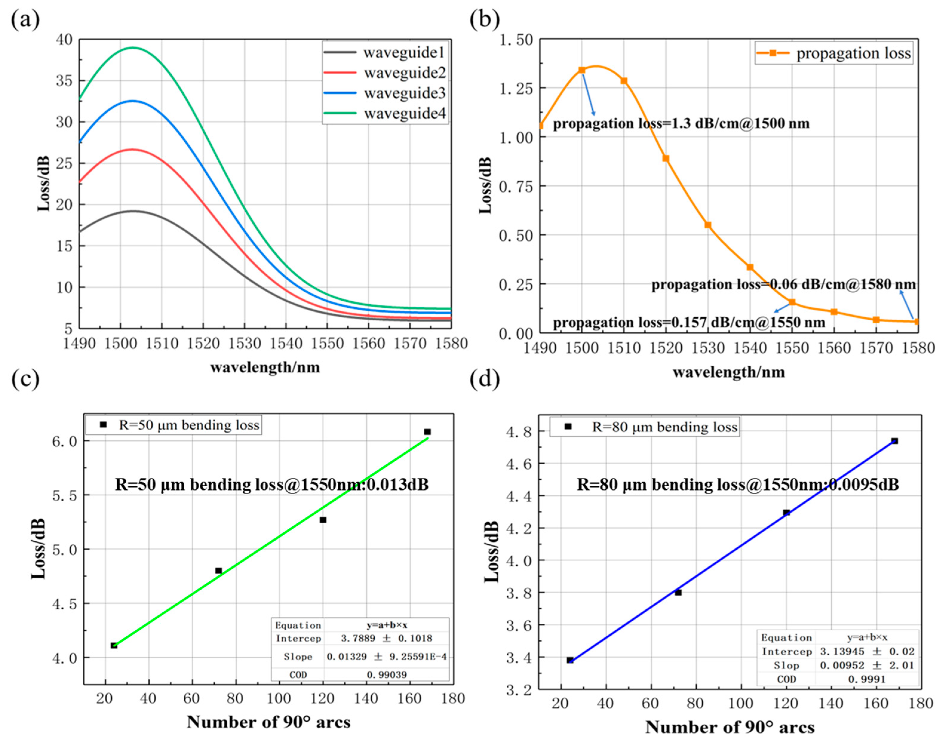
4. Device Characterization and Discussion

After the fabrication, we characterized the basic performance of the waveguide, including propagation loss and bending loss. The test platform is shown in Figure 12c; the light source was a tunable laser covering the whole C-band (model: Keysight 8164B). A lensed single-mode fiber was used to couple the light from the laser into the waveguide, and another lensed fiber was used to couple the light out of the waveguide to a power detector. A cutback structure, as shown in Figure 12d, was used to measure the propagation loss. Considering the low loss of the Si3N4 waveguide, we increased the length of each waveguide in the cutback structures; the parameters needed to accumulate enough propagation loss are shown in Table 2. Due to similar considerations, a set of waveguides with a different number of bends are used to measure the bending loss; parameters are shown in Table 3.
For measurement of the propagation loss and bending of the Si3N4 waveguide, the transmission loss of the Si3N4 waveguides was scanned in the wavelength range 1490–1580 nm. The wavelength response of the cutback structures is shown in Figure 13a. Through linear fitting of the data, the propagation loss in the same wavelength range can be calculated as the results shown in Figure 13b. It can be seen that the propagation loss of the waveguide has a peak of 1.33 dB/cm at a wavelength of around 1500 nm, which is due to the absorption loss of the Si-H bonding in the Si3N4. To reduce this loss, annealing with a higher temperature and longer time is needed to further repel the H element in the film. As the wavelength moves away from the absorption band, the propagation loss reduces quickly to transmission of 0.157 dB/cm at 1550 nm and 0.06 dB/cm at 1580 nm. This is a remarkable value compared to other reported works, as summarized in Table 4.
We further measured the bending loss by fitting the transmission spectrum of waveguides with a different number of bends. The results are shown in Figure 13c,d for two different bending radii; the bending loss is 0.0095 dB per 90° bending waveguide for a radius of 80 µm and 0.013 dB even for a radius of 50 µm, which is very close to the previous simulations.
Table 4 summarizes the results of other groups and this work. It is clear that the Si3N4 waveguide with LPCVD has a lower loss than that of PECVD. Compared to other works with LPCVD, this work is state of the art, especially on an 8-inch wafer.

5. Conclusions

In order to solve the problem of high stress caused by the preparation of thick silicon nitride waveguides (≥300 nm) via LPCVD, this work used the filling of silicon nitride in the BOX layer trench to prepare waveguides. For the deposition of the core layer, we used a vertical furnace tube with a rotating holder during the deposition of the film, which prevented the accumulation of stress in one direction. At the same time, in order to reduce the stress, we set up a checkerboard stress relief pattern in the BOX layer; to make the CMP more uniform and reduce the warpage of the wafer, we removed all the silicon nitride in the nonwaveguide area before the CMP. Based on all these optimizations, we successfully demonstrated Si3N4 waveguides with LPCVD on an 8-inch wafer. This showed brilliant loss properties with a propagation loss of 0.157 dB/cm at 1550 nm and 0.06 dB/cm at 1580 nm. The bending loss is also characterized by 0.013 dB at a radius of 50 μm and only 0.0095 dB at a radius of 80 μm. All the results meet the state-of-the-art specifications with a similar process.

Author Contributions

Conceptualization, Z.L.; data curation, Z.L., Q.C. and J.Z.; formal analysis, Z.L. and Z.F.; investigation, Z.L. and X.Z.; methodology, Z.L., Y.Z. and L.J.; resources, L.J. and Z.L.; software Z.L. and Z.F.; supervision, L.J. and Y.Z.; writing—original draft, Z.L.; writing—review and editing, L.J., Z.F. and X.Z. All authors have read and agreed to the published version of the manuscript.

Funding

This document is the result of the research project funded by the National Key Research and Development Program Funding Project (2018YFB2200503).

Institutional Review Board Statement

Not applicable.

Informed Consent Statement

Not applicable.

Data Availability Statement

Not applicable.

Acknowledgments

We thank Liming Lv, Yiyi Wang, and Yawen Li for their technical support and suggestive discussions.

Conflicts of Interest

The authors declare no conflict of interest.

References

  1. Blumenthal, D.J.; Rene, H.; Douwe, G.; Arne, L.; Chris, R. Silicon Nitride in Silicon Photonics. Proc. IEEE 2018, 106, 2209–2231. [Google Scholar] [CrossRef] [Green Version]
  2. Mao, S.C.; Tao, S.H.; Xu, Y.L.; Sun, X.W.; Yu, M.B.; Lo, G.Q.; Kwong, D.L. Low Propagation Loss Sin Optical Waveguide Prepared by Optimal Low-Hydrogen Module. Opt. Express 2008, 16, 20809–20816. [Google Scholar] [CrossRef] [PubMed] [Green Version]
  3. Ikeda, K.; Robert, E.S.; Nikola, A.; Yeshaiahu, F.T. Kerr Nonlinear Properties of Plasma-Deposited Silicon Nitride/Silicon Dioxide Waveguides. Opt. Express 2008, 16, 12987–12994. [Google Scholar] [CrossRef] [PubMed] [Green Version]
  4. Su, Y.; Yong, Z.; Qiu, C.; Guo, X.; Lu, S. Silicon Photonic Platform for Passive Waveguide Devices: Materials, Fabrication, and Applications. Adv. Mater. Technol. 2020, 5, 1901153. [Google Scholar] [CrossRef]
  5. Ji, X.; Samantha, R.; Mateus, C.-Z.; Michal, L. Methods to Achieve Ultra-High Quality Factor Silicon Nitride Resonators. APL Photonics 2021, 6, 071101. [Google Scholar] [CrossRef]
  6. Shastri, B.J.; Alexander, N.T.; de Lima, T.F.; Wolfram, H.P.P.; Harish, B.; Wright, C.D.; Prucnal, P.R. Photonics for Artificial Intelligence and Neuromorphic Computing. Nat. Photonics 2021, 15, 102–114. [Google Scholar] [CrossRef]
  7. Pfeifle, J.; Brasch, V.; Lauermann, M.; Yu, Y.; Wegner, D.; Herr, T.; Hartinger, K.; Schindler, P.; Li, J.; Hillerkuss, D.; et al. Coherent Terabit Communications with Microresonator Kerr Frequency Combs. Nat. Photonics 2014, 8, 375–380. [Google Scholar] [CrossRef] [Green Version]
  8. Poot, M.; Schuck, C.; Ma, X.-S.; Guo, X.; Tang, H.X. Design and Characterization of Integrated Components for Sin Photonic Quantum Circuits. Opt. Express 2016, 24, 6843–6860. [Google Scholar] [CrossRef] [Green Version]
  9. Yu, M.; Okawachi, Y.; Joshi, C.; Ji, X.; Lipson, M.; Gaeta, A.L. Gas-Phase Microresonator-Based Comb Spectroscopy without an External Pump Laser. ACS Photonics 2018, 5, 2780–2785. [Google Scholar] [CrossRef] [Green Version]
  10. Li, D.; Li, B.; Tang, B.; Zhang, P.; Yang, Y.; Liu, R.; Xie, L.; Li, Z. Broadband Silicon Nitride Power Splitter Based on Bent Directional Couplers with Low Thermal Sensitivity. Micromachines 2022, 13, 559. [Google Scholar] [CrossRef]
  11. Jiang, W.; Xu, D.; Yao, S.; Xiong, B.; Wang, Y. Effect of Hyperthermal Annealing on Lpcvd Silicon Nitride. Mater. Sci. Semicond. Process. 2016, 43, 222–229. [Google Scholar] [CrossRef]
  12. Li, B.; Li, D.; Tang, B.; Zhang, P.; Yang, Y.; Liu, R.; Xie, L.; Li, Z. Towards Monolithic Low-Loss Silicon Nitride Waveguides on a Mature 200 mm Cmos Platform. Optik 2022, 250, 168309. [Google Scholar] [CrossRef]
  13. Xuan, Y.; Liu, Y.; Varghese, L.T.; Metcalf, A.J.; Xue, X.; Wang, P.-H.; Han, K.; Jaramillo-Villegas, J.A.; Al Noman, A.; Wang, C.; et al. High-Q Silicon Nitride Microresonators Exhibiting Low-Power Frequency Comb Initiation. Optica 2016, 3, 1171–1180. [Google Scholar] [CrossRef] [Green Version]
  14. Krückel, C.J.; Fülöp, A.; Ye, Z.; Andrekson, P.A.; Torres-Company, V. Optical Bandgap Engineering in Nonlinear Silicon Nitride Waveguides. Opt. Express 2017, 25, 15370–15380. [Google Scholar] [CrossRef] [Green Version]
  15. Olson, J.M. Analysis of Lpcvd Process Conditions for the Deposition of Low Stress Silicon Nitride. Part I: Preliminary Lpcvd Experiments. Mater. Sci. Semicond. Process. 2002, 5, 51–60. [Google Scholar] [CrossRef]
  16. Sharma, N.; Hooda, M.; Sharma, S.K. Synthesis and Characterization of Lpcvd Polysilicon and Silicon Nitride Thin Films for Mems Applications. J. Mater. 2014, 2014, 954618. [Google Scholar] [CrossRef] [Green Version]
  17. Chen, K.-S. Techniques in Residual Stress Measurement for Mems and Their Applications. In Mems/Nems: Handbook Techniques and Applications; Cornelius, T.L., Ed.; Springer US: Boston, MA, USA, 2006; pp. 1252–1328. [Google Scholar]
  18. De Oliveira, E.C.; Gerosa, R.M.; Phelan, C.; de Matos, C.J.S. Fabrication and Characterization of Silicon Nitride Waveguides for Mid-Infrared Applications. In Proceedings of the 2019 SBFoton International Optics and Photonics Conference (SBFoton IOPC), Sao Paulo, Brazil, 7–9 October 2019. [Google Scholar]
  19. Shang, K.; Pathak, S.; Guan, B.; Liu, G.; Yoo, S.J.B. Low-Loss Compact Multilayer Silicon Nitride Platform for 3d Photonic Integrated Circuits. Opt. Express 2015, 23, 21334–21342. [Google Scholar] [CrossRef] [Green Version]
  20. Muñoz, P.; Doménech, J.; Domínguez, C.; Sánchez, A.; Micó, G.; Bru, L.; Pérez, D.; Pastor, D. State of the Art of Silicon Nitride Photonics Integration Platforms. In Proceedings of the 2017 19th International Conference on Transparent Optical Networks (ICTON), Girona, Spain, 2–6 July 2017. [Google Scholar]
  21. Krückel, C.J.; Fülöp, A.; Klintberg, T.; Bengtsson, J.; Andrekson, P.A.; Torres-Company, V. Linear and Nonlinear Characterization of Low-Stress High-Confinement Silicon-Rich Nitride Waveguides. Opt. Express 2015, 23, 25827–25837. [Google Scholar] [CrossRef] [Green Version]
  22. Wörhoff, K.; Heideman, R.G.; Arne, L.; Marcel, H. Triplex: A Versatile Dielectric Photonic Platform. Adv. Opt. Technol. 2015, 4, 189–207. [Google Scholar] [CrossRef]
  23. Roeloffzen, C.G.H.; Hoekman, M.; Klein, E.J.; Wevers, L.S.; Timens, R.B.; Marchenko, D.; Geskus, D.; Dekker, R.; Alippi, A.; Grootjans, R.; et al. Low-Loss Si3N4 Triplex Optical Waveguides: Technology and Applications Overview. IEEE J. Sel. Top. Quantum Electron. 2018, 24, 4400321. [Google Scholar] [CrossRef] [Green Version]
  24. Haddadan, F.; Soroosh, M. Design and Simulation of a Subwavelength 4-to-2 Graphene-Based Plasmonic Priority Encoder. Opt. Laser Technol. 2023, 157, 108680. [Google Scholar] [CrossRef]
  25. Maleki, M.; Soroosh, M.; Akbarizadeh, G. A Subwavelength Graphene Surface Plasmon Polariton-Based Decoder. Diam. Relat. Mater. 2023, 134, 109780. [Google Scholar] [CrossRef]
  26. Mu, X.; Wu, S.; Cheng, L.; Fu, H. Edge Couplers in Silicon Photonic Integrated Circuits: A Review. Appl. Sci. 2020, 10, 1538. [Google Scholar] [CrossRef] [Green Version]
  27. Ren, G.; Chen, S.; Cheng, Y.; Zhai, Y. Study on Inverse Taper Based Mode Transformer for Low Loss Coupling between Silicon Wire Waveguide and Lensed Fiber. Opt. Commun. 2011, 284, 4782–4788. [Google Scholar] [CrossRef]
  28. Roelkens, G.; Vermeulen, D.; Selvaraja, S.; Halir, R.; Bogaerts, W.; Van Thourhout, D. Grating-Based Optical Fiber Interfaces for Silicon-on-Insulator Photonic Integrated Circuits. IEEE J. Sel. Top. Quantum Electron. 2011, 17, 571–580. [Google Scholar] [CrossRef] [Green Version]
  29. Park, T.; Son, C.; Kim, T.; Lim, S. Understanding of Si3N4-H3PO4 Reaction Chemistry for the Control of Si3N4 Dissolution Kinetics. J. Ind. Eng. Chem. 2021, 102, 146–154. [Google Scholar] [CrossRef]
  30. Henry, C.H.; Kazarinov, R.F.; Lee, H.J.; Orlowsky, K.J.; Katz, L.E. Low Loss Si3N4–SiO2 Optical Waveguides on Si. Appl. Opt. 1987, 26, 2621–2624. [Google Scholar] [CrossRef]
  31. Wang, L.; Xie, W.; Van Thourhout, D.; Zhang, Y.; Yu, H.; Wang, S.H. Nonlinear Silicon Nitride Waveguides Based on a Pecvd Deposition Platform. Opt. Express 2018, 26, 9645–9654. [Google Scholar] [CrossRef] [Green Version]
  32. Epping, J.P.; Hoekman, M.; Mateman, R.; Leinse, A.; Heideman, R.; van Rees, A.; van der Slot, P.J.; Lee, C.J.; Boller, K.J. High Confinement, High Yield Si3N4 Waveguides for Nonlinear Optical Applications. Opt. Express 2015, 23, 642–648. [Google Scholar] [CrossRef] [Green Version]
  33. Pfeiffer, M.H.P.; Clemens, H.; Liu, J.; Tiago, M.; Michael, Z.; Michael, G.; Tobias, J.K. Photonic Damascene Process for Low-Loss, High-Confinement Silicon Nitride Waveguides. IEEE J. Sel. Top. Quantum Electron. 2018, 24, 6101411. [Google Scholar] [CrossRef]
Figure 1. (a) Schematic cross-section of a rectangular Si3N4 waveguide, (b) Schematic of light transmission in the waveguide.
Applsci 13 03660 g001
Figure 2. The simulation curve of the effective refractive index under different waveguide widths.
Applsci 13 03660 g002
Figure 3. The simulation curve of the waveguide bending loss per 90° under different bending radii.
Applsci 13 03660 g003
Figure 4. Schematic of inverse tapered edge coupler.
Applsci 13 03660 g004
Figure 5. The simulation curve of the coupling efficiency at different widths (a) Wtaper and (b) Ltaper.
Applsci 13 03660 g005
Figure 6. The field distribution of the light transmission in the inverse tapered edge coupler at 1550 nm.
Applsci 13 03660 g006
Figure 7. The fabrication process flow of the Si3N4 waveguide. (a) wafer start on a 8-inch wafer; (b) BOX layer deposition; (c) HM deposition and lithography; (d) HM etch; (e) BOX layer etch; (f) BOX layer anneal; (g) core layer deposition; (h) reverse etch; (i) CMP; (j) core layer anneal; (k) cladding layer deposition.
Applsci 13 03660 g007
Figure 8. (a) Layout design of the checkerboard stress relief pattern; (b) SEM images of the checkerboard stress relief pattern.
Applsci 13 03660 g008
Figure 9. SEM images of the etched waveguide pattern in the BOX.
Applsci 13 03660 g009
Figure 10. SEM images of the waveguide structure after HM removal. (a) partially removed HM, (b) fully removed HM.
Applsci 13 03660 g010
Figure 11. (a) XSEM image of the waveguide with measured dimensions, (b) XSEM image of two adjacent waveguides observed after cutting through with FIB, (c) SEM image of the tip after CMP, (d) SEM image of the waveguide after CMP.
Applsci 13 03660 g011
Figure 12. (a) Finished 8-inch wafers, (b) silicon nitride chips, (c) semi-automatic test platform, (d) layout design of the spiral and bending waveguides for the test.
Applsci 13 03660 g012
Figure 13. The measurement result of the Si3N4 waveguide with a cross-sectional size of 0.4 μm × 1 μm (a) the transmission loss of the cutback structure in the wavelength range of 1490–1580 nm, (b) the fitted propagation loss in the wavelength range of 1490–1580 nm, (c) the fitting line of bending loss @1550 nm per 90° bending waveguide for a radius of 50 μm, (d) the fitting line of bending loss @1550 nm per 90° bending waveguide for a radius of 80 μm.
Applsci 13 03660 g013
Table 1. Structural dimensions of the inverse tapered edge coupler.
Structural ParametersSize
Wtaper0.3 μm
WWG1.0 μm
Ltaper200 μm
Table 2. Structural parameters of the cutback structure.
No.LengthRadius of Bending Waveguide
waveguide 112.72 cmR = 100 μm
waveguide 217.62 cmR = 100 μm
waveguide 322.52 cmR = 100 μm
waveguide 427.42 cmR = 100 μm
Table 3. Structural parameters of the bending waveguides.
Radius of Bending WaveguideNo.Number of 90° Arcs
50 μmbend124
bend272
bend3120
bend4168
80 μmbend124
bend272
bend3120
bend4168
Table 4. Summary of propagation losses at 1550 nm for Si3N4 waveguides.
Ref.Waveguide Height × Width (μm)Wafer SizePropagation Loss (dB/cm)Deposition
[2]0.4 × 0.782.1PECVD
[12]0.4 × 1.080.62LPCVD
[21]0.7 × 1.6541.0LPCVD
[31]0.6 × 1.583.75PECVD
[32]0.9 × 0.840.4LPCVD
[33]0.77 × 1.7540.05LPCVD
This work0.4 × 1.080.157LPCVD
Disclaimer/Publisher’s Note: The statements, opinions and data contained in all publications are solely those of the individual author(s) and contributor(s) and not of MDPI and/or the editor(s). MDPI and/or the editor(s) disclaim responsibility for any injury to people or property resulting from any ideas, methods, instructions or products referred to in the content.

