Article

Research of Tri-State Optical Signal Detectors for Ternary Optical Computers

1
School of Computer Engineering and Science, Shanghai University, Shanghai 200444, China
2
School of Computer Science and Artificial Intelligence, Chaohu University, Hefei 238024, China
3
College of Computer Science and Technology, Hainan Tropical Ocean University, Sanya 572022, China
*
Author to whom correspondence should be addressed.
Appl. Sci. 2023, 13(5), 2800; https://doi.org/10.3390/app13052800
Submission received: 14 January 2023 / Revised: 17 February 2023 / Accepted: 19 February 2023 / Published: 22 February 2023

Abstract

:
A tri-state optical signal detector (TOD) is designed in this article to improve the accuracy and stability of decoding results of the ternary optical computer (TOC). The TOD consists of three modules: a light-sensing module, a voltage divider module, and a data latching and conversion module. First, a voltage divider circuit with adjustable resistors is used to achieve parallel optical–electrical signal conversion for each LCD pixel on a photosensitive sensor plus a latch structure. Second, the problem of the parallel storage of data after photoelectric conversion is solved. Third, a transcoding circuit from the output signal of the TOD to the input signal of the tri-state optical encoder (TOE) is given. The experimental results show that the tri-state optical signal detector designed in this paper is effective and feasible.

1. Introduction

As the research on ternary optical processors has intensified [1,2,3,4,5,6,7,8], TOCs have moved into the stage of application [9,10]. Each TOC has a large number of processor bits, and the processor bits are divisible, spliceable, and reconfigurable for computational functions. Considering the current user habits of electronic computers, the advantages of both optical computers and electronic computers can be brought into full play by working together. Therefore, it is necessary to follow the non-computing components such as the peripheral, control, and storage components used in modern electronic computers as much as possible, meaning the physical method of expressing information must allow fast conversion between optical and electrical signals. Based on this background, and under continuous research, an encoder that enables electrooptical signal conversion [1,11,12] was integrated with the TOC, while the TOD (also called decoder) that enables electro-optical signal conversion remains independent of the TOC.
The studies on decoders have proceeded as follows. The structure and working principle of a tri-state optical signal detector using a light-sensing unit for photoelectric conversion were first proposed by Jin [1]. Sun [11,13] completed the experiment by decoding one bit of three-value light after using the commonly used separation element (i.e., spinner) for light separation. Zuo [14] investigated the problems with the high-speed, reliable, and real-time sampling and image acquisition of optical operator results using an optical decoding simulator, and designed a USB-type image acquisition system, followed by the implementation of a decoding system for a three-value optical computer using a CMOS image sensor and an embedded system [15]. Xue [16] designed a data acquisition control system according to the decoder’s data acquisition characteristics, and performed automatic control, data transmission, status management, and data display for the decoder. The above studies for tri-state optical signal detectors have all involved serial decoding. Yehqiang [17] proposed a parallel photoreceptor array decoder designed for the SD11 (composed of the Chinese abbreviation of Shanghai University and the machine number). The paper proposes a method of detecting and latching the state of the light signal using a phototube plus latch structure, achieving the first fully parallel photoreceptor decoding process. However, the parallel photoreceptor array decoder is only for the SD11 system, and two sets of the same detection structure must be used to judge the output result of one operator bit, which greatly increases the production cost of the decoder.
The commercially available photoelectric conversion devices [18,19] are not suitable for TOCs, so the decoder system can only be developed by the team independently. The current decoder uses a camera to capture the result picture of the optical computer, and then transmits this back to the electronic computer via the software to decode the gray value of the picture. The decoding result is then sent to the optical computer for the next calculation, and the above process is repeated until the end of the operation, when the final result is transmitted to the electronic computer. The whole process is slow and less stable, which is the biggest obstacle to improving the overall performance of the TOC and achieving integrated manufacturing. To solve the above problems, the authors studied the current TOC prototype, the SD16 system, and designed a tri-state optical signal detector to remove the last obstacle for the integrated manufacturing of the TOC, naming the TOC equipped with this detector SD22.

2. Materials and Methods

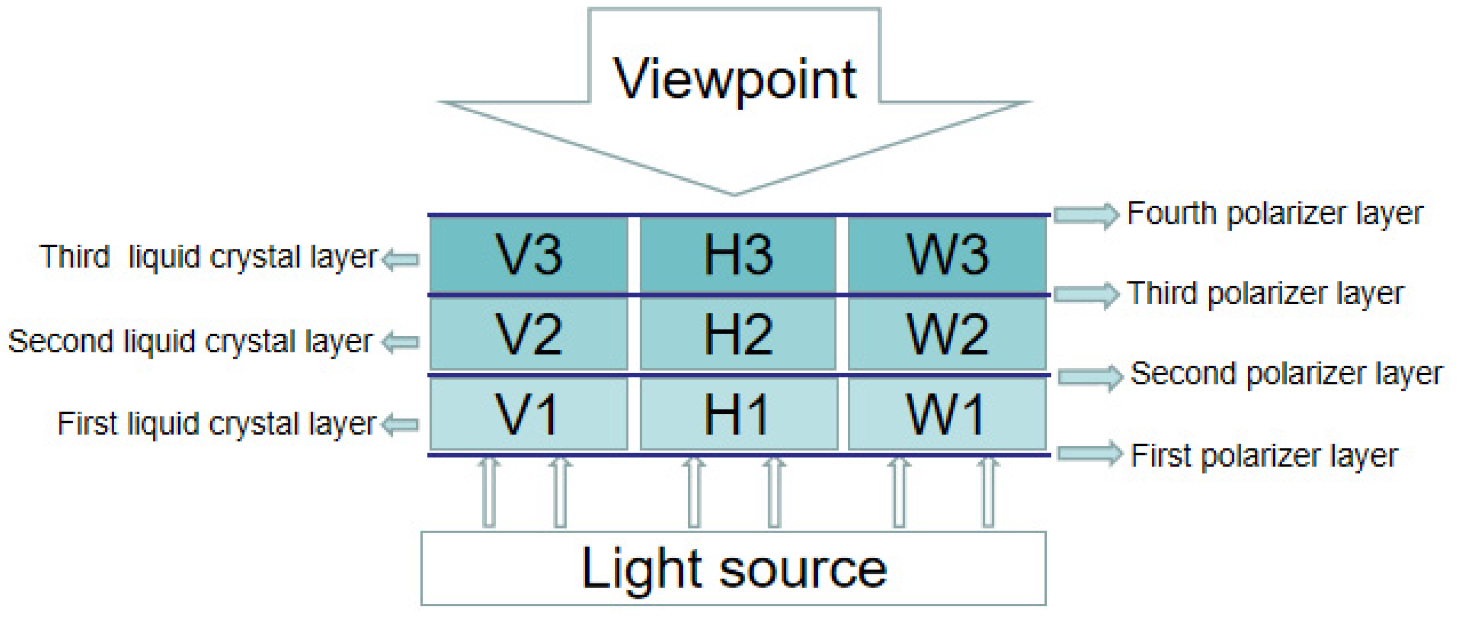
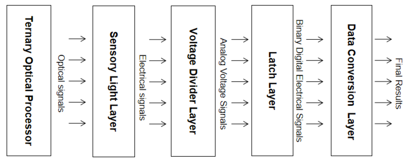
2.1. Structure of the Ternary Optical Processor

The TOC uses null light (W), horizontally polarized light (H), or vertically polarized light (V) to represent the three-value information. In SD16, one processor bit consists of four layers of polarizers sandwiched by three layers of liquid crystals, and 192 processor bits constitute a module of the optical operator of SD16 [20]. The structure of the processor bits is shown in Figure 1.
The first, second, and third layers of polarizers are vertically polarized and can only pass vertically polarized light. The polarization orientation of the fourth polarizer is about 30 degrees from the vertical direction, and its function is to convert the two light signals with an orthogonal polarization direction from the operator to two different brightness levels. The polarization orientation of the fourth polarizer is about 30 degrees from the vertical direction, and its function is to convert the two light signals with orthogonal polarization direction from the operator to two different brightness levels.
Since the liquid crystals from columns V, H, and W in Figure 1 have the same function, this paper takes column V’s liquid crystals as an example; when the signal of the control light path is not considered, there are two types of rotation modes for each layer of liquid crystals, so there are 8 types of rotation modes for three layers of liquid crystals, and the corresponding output light state and light brightness of the 8 types of rotation modes are given in Table 1.
The polarizer used in SD16 does not absorb blue light, and because of the angle of the polarizer, when the final result of the optical processor is observed with the naked eye, the V light is white, the H light is light green, and the W light is blue, as shown in Figure 2. Figure 2 shows the top view of the whole optical processor, consisting of 192 operator bits, each with 3 columns of pixels, so there are 576 liquid crystal pixels from the top view.

2.2. Theory of Three-State Optical Signal Detectors

2.2.1. Photoelectric Conversion

The main objective of this study is to accurately convert the 576 polarized optical signals from an optical operator to the corresponding electrical signals.
Ideally, the same polarized light would be presented with the same light intensity on the top LCD of each processor bit. The optical operator of the SD16 uses a backlight board as the light source [12], which in theory should be a uniform-intensity light source. However, the structure of the backlight board determines that it is not a uniform light source. There are seven LED beads inside the backlight board, and their positions are shown in Figure 3. They are concentrated on one edge of the backlight board, and the light source of the LED beads is reflected to other parts of the backlight board through the internal reflection film. This causes the light intensity near the LED beads to be stronger, while away from the LED beads, the light intensity is weaker, ultimately presenting the inconsistent light intensity of the LCD pixels.
Since the actual light intensity of the liquid crystal pixels is not uniform, this study uses “point-to-point sensing”, i.e., each liquid crystal pixel has its own corresponding photosensitive sensor and photoelectric conversion circuit. An LCD pixel will present three light intensities, so two bits of data are needed to represent them. In this paper, we specify 11 for V light, 10 for H light, and 00 for W light.
According to this provision, this paper uses a voltage divider circuit in the photoelectric conversion circuit part to process the electrical signal from the photosensitive sensor, and the specific circuit implementation will be described in detail in Section 2.3.1.

2.2.2. Data Conversion

The polarization state of the optical processor becomes a set of raw electrical signals after the photoelectric conversion, which still needs to be transcoded to become the input of the optical encoder or the final output that is transmitted back to the electronic computer. In SD16, the input data of the tri-state optical encoder is represented by 10 for V-light, 01 for H-light, and 00 for W-light, while the decoder output of one processor bit requires 6 bits of data for V-light, H-light, and W-light.
Since V-light and H-light do not appear simultaneously in three LCD pixels of one processor bit, we provide the tri-state light signal detector output data, tri-state light encoder input data, and the correspondence between the three states of light, as shown in Table 2.
According to Table 2, we propose a circuit logic structure to convert the decoder output of one processor bit to the encoder input, as shown in Figure 4. In Figure 4, A~F correspond to the outputs of the tri-state optical signal detectors in Table 2, G and H are the output signals of the input data after the or gate, Z and N correspond to the inputs of the tri-state optical encoders in Table 2.

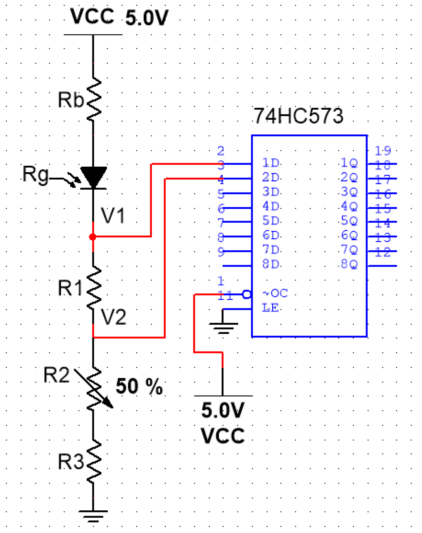
2.3. Design of Three-State Optical Signal Detectors

2.3.1. Design of Decoding Circuit for One LCD Pixel

The decoding circuit of one pixel is shown in Figure 5, where Rb is the protective resistor of the photosensitive sensor Rg, which senses the light intensity of the liquid crystal. When the liquid crystal pixels show different polarization states, the electric current information from Rg is different, i.e., the current through Rg is positively correlated with the light intensity. First, we connect two fixed circuits R1 and R3 at the negative terminal of Rg and access the adjustable resistor R2 in the middle of the two fixed resistors. We set the voltage divider output points V1 and V2 in the middle of Rg and R1, and R1 and R2. We connect V1 and V2 to inputs 1D and 2D of latch 74HC573. The addition of the adjustable resistor R2 improves the flexibility and fault tolerance of the circuit.
The circuit can be described as follows. When the measured pixel is white, V1 > V2 > 3.5 V, and the latch output is 11; when the measured pixel is light green, V1 > 3.5 V, V2 < 3.5 V, and the latch output is 10; when the measured pixel is blue, V2 < V1 < 3.5 V, and the latch output is 00.

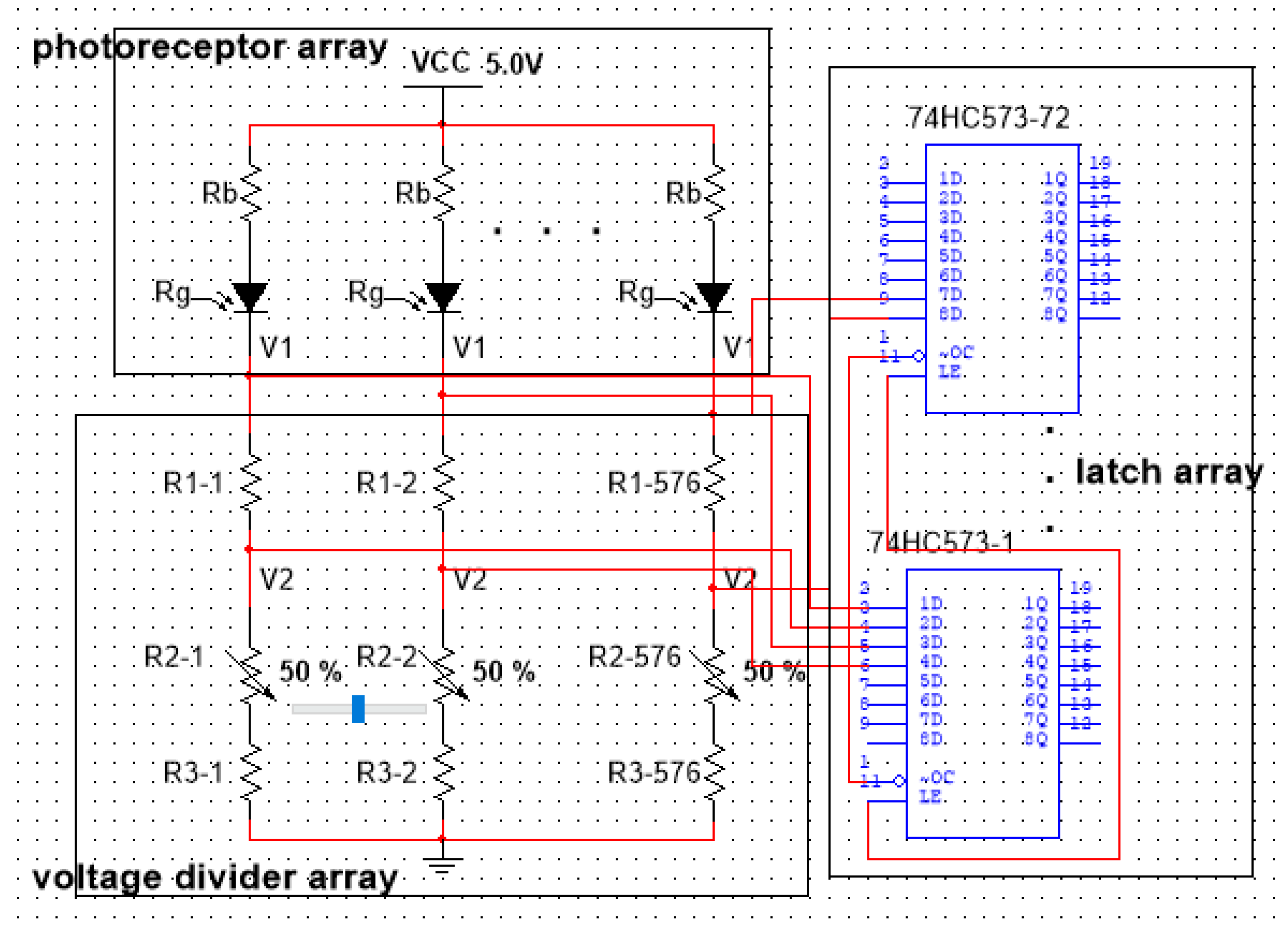
2.3.2. Parallel Design of 576-Bit LCD Pixel Decoding Circuit

The tri-state optical signal detector is composed of 576 one-bit pixel decoding circuits connected in parallel, as shown in Figure 6. In Figure 6, there is a percentage that represents the ratio of the actual resistance of the adjustable resistor to the maximum resistance, where 50% means that the resistance of this adjustable resistor is half of the maximum resistance. In the actual circuit, we will adjust this ratio as needed.
The parallel circuit can be divided into three arrays: the photoreceptor array, voltage divider array, and latch array. The photoreceptor array consists of 576 parallel-connected photosensitive sensors. The voltage divider array is responsible for the conversion of the electrical signals acquired by the photoreceptor array, while the input active terminal OE and the output active terminal LE of all latches in the latch array are connected in parallel, which can allow the complete synchronization of the operation timing. Considering the workload of this experiment, only the decoder is discussed here to obtain the valid photoelectric conversion information, and the output part of the latching array is omitted in Figure 6. Due to the large number of components in the decoder, a layered design was carried out for the physical design.

2.3.3. Layered Design of Tri-State Optical Signal Detector

The hierarchical design idea for the tri-state optical signal detector is shown in Figure 7.
The first layer is the light-sensitive layer. Each photosensitive sensor on the light-sensitive layer corresponds to the liquid crystal pixels of the optical processor and is mainly responsible for converting light signals into electrical signals. Considering the maintenance convenience and cost, we adopt the stitching idea proposed by Shi Yehqiang [17]; that is, 16 photoreceptor circuits form a photoreceptor module with a small-scale integration degree, and then 36 photoreceptor modules are stitched together to form the whole photoreceptor layer. Therefore, if any component is damaged, you only need to replace the small module where the damaged component is located.
The second layer is the voltage divider resistor layer; the purpose of this layer is to divide the current information obtained from the conversion of the photoreceptor layer and obtain the electrical signal corresponding to the light intensity information of the liquid crystal pixels. The third layer is the latch layer, where the latch-active LE and the output-active OE of the latch are connected in parallel and controlled by signals. After the LE receives a valid latch signal, the latch will simultaneously latch the electrical signal from the voltage divider resistor layer, and then output the latch “1” and “0” information after the OE receives a valid signal from the output. The fourth layer is the data conversion layer, the function of which is to convert the decoded raw data coming from the latch layer into the input of the optical encoder. If the decoding result is already finalized at this point, the final result is output directly to the electronic computer.
Since the functions of the latch layer and data conversion layer can be performed by FPGA, the physical design of the three-state optical signal detector focuses on the first two layers. Considering the splicing problem, the two layers are subdivided into the photoreceptor layer, protective resistor layer, and voltage divider resistor layer, and the layers are connected by connectors, as shown in Figure 8.
In Figure 8, the photoreceptor layer consists of 36 small photoreceptor modules, each of which is mounted to the protective resistive layer using pins. It should be noted that the photosensitive sensor on the photosensitive layer needs to be aligned with the liquid crystal pixels. The protective resistor layer and the voltage divider resistor layer are connected vertically, and there are more connection lines between the layers, so the connector used is a 288-pin memory slot. The memory slot is installed in the protective resistor layer, so the interface will be designed in the form of a memory stick when designing the voltage divider resistor layer. For subsequent installations, Figure 8 will be rotated 90 degrees counterclockwise for physical installations.

3. Results

This experiment was conducted on the SD16 system, which is shown in Figure 9. The purpose of the experiment was to obtain the range of voltage divider resistance values and record them to determine the size of the adjustable resistors that should be installed in the decoding circuit of each partition, and finally to achieve the accurate decoding of the brightness of each LCD pixel.

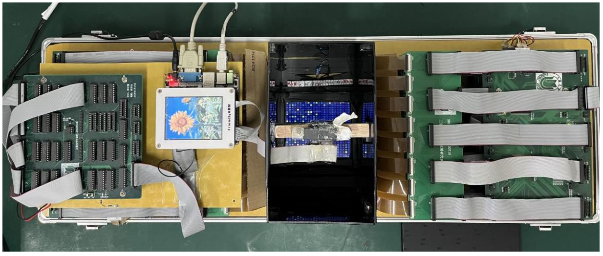
3.1. Experimental Preparation and Experimental Steps

Before the experiment, 576 liquid crystal pixels were divided into 9 regions according to the mounting position of the light source of the optical operator, and selected test points within each region according to the distance from the light source, as shown in Figure 10. The light source is not photographed in Figure 10 because the light source was hidden at the time of production, and the reader should note that the actual light source is shown directly above in Figure 10.
The position of the light source is above the liquid crystal array shown in Figure 10, so region 2 is closest to the light source and has the strongest light intensity; regions 1 and 3 are on both sides of the light source and have slightly weaker light intensity; region 5 is at a suitable distance from the light source and has stable light intensity; regions 4, 6, 7, 8 and 9, are farther away from the light source and have weaker light intensity. This experiment produced nine mutually independent tri-state light signal detection circuits, the purpose of which is firstly to correspond to the partition; secondly to test the discrete nature, stability, and sensitivity of the light-sensitive sensor used in the experiment; and thirdly so that the independent light-sensitive circuit can be flexibly moved on the pixels in the area to which it belongs to facilitate the experiment.
In this experiment, a CXDSMD023 photosensitive sensor model was used to make a light-sensitive tube, and tape was wrapped around the top to shade the light, as shown in Figure 11.
In the experiment, the tube is fixed above the liquid crystal pixel, and the vertical distance between the tube and the liquid crystal is about 1 mm. After the preparation process, the optical processor will randomly output the calculation results used for the test, followed by the tri-state optical signal detector for the display of its corresponding LCD pixels for photoelectric signal conversion. If the LCD pixel shows white light, the latch will eventually output 11; if the LCD pixel shows light green light, the latch will eventually output 10; if the LCD pixel shows blue light, the latch will eventually output 00. Next, the corresponding voltage dividing resistance value of the LCD pixels in each area is determined, and the adjustable resistor is adjusted according to the output of the latch during the experiment, so that the latch finally outputs the correct result.
For recording purposes, each LCD pixel is numbered. Using the numbered bits of the optical operator processor bits as a reference, an example of the liquid crystal numbering of processor bit 0 and processor bit 1 can be given, where from left to right the liquid crystal pixels are numbered 0–1, 0–2, 0–3, 1–1, 1–2, and 1–3, and the processor bits are numbered as shown in Figure 12.
After numbering the liquid crystal pixels, we can record the code of the liquid crystal pixel selected for the experiment in each sub-area in the experimental record book and perform the following experimental steps:
  • We use a 5 V power supply for the nine detection circuits, and the photoreceptor circuit latch input enables terminal LE in parallel, using an electrical signal control, while the output of each latch OE is also connected in parallel to the ground, so that it is effective. The latch output is connected to a multimeter tuned to the voltage range, which makes it more intuitive to view the values and easy to adjust the resistance values of the adjustable resistors;
  • We fix the head of the tube at 1 mm directly above the LCD pixel;
  • The optical processor randomly outputs the test results and sends an input enable signal to the latch, which latches the signal and outputs it, and the output result is the voltage value displayed on the multimeter;
  • We record the resistance value and voltage value of each photoreceptor circuit. If the collected LCD pixels are white, the latch should output 11, corresponding to voltage values of the multimeter of 3.5 V with 3.5 V; if this is not correct, then we can adjust the resistance value until the output is correct and record this resistance value. If the collected LCD pixel is a light green light, the latch should output 10, corresponding to a voltage value of the multimeter of 3.5 V with the actual voltage value (not the full 3.5 V); if this is not correct, then we can adjust the resistance value until the output is correct and record the resistance value. If the collected LCD pixels are blue, the latch should output 00, corresponding to the voltage values of the multimeter, which should be two actual voltage values (not the full 3.5 V); if this is not correct, then we can adjust the resistance value until the output is correct and record the resistance value;
  • We repeat step 2, move the photosensitive sensor of the detection circuit to the next liquid crystal pixel, and repeat steps 3 and 4 until the voltage dividing resistance portion of the selected liquid crystal pixel is adjusted;
  • We repeat the test 3 times for all data, and take the minimum resistance value and the maximum resistance value.

3.2. Experimental Results

According to the above experimental steps, the results of the random output of the optical processor were tested repeatedly to obtain the data in Table 3.
The minimum and maximum resistance values recorded in Table 3 are related to the brightness and darkness of the LCD pixels. Low resistance means stronger light intensity and large resistance means stronger light intensity.
Taking into account the existence of errors and according to the data in the table, we reduced the fixed resistance of each area of the voltage divider resistor layer by a certain percentage and enlarged the adjustable resistor resistance by a certain percentage, then determined the resistance value in each area as follows:
  • In the corner of the 3, 7, 9 test area, the weakest light intensity can be set to R1 by a 100 K fixed resistance, R2 is set to a 1 M adjustable resistance, and R3 is set to a 500 K fixed resistance;
  • In the edge of the 2, 4, 6, 8 test area, the light intensity is slightly stronger, R1 can be set to a 50 K fixed resistor, R2 is set to a 1 M adjustable resistor, and R3 is set to a 400 K fixed resistor;
  • Near the light source in the area of 1, 5, the liquid crystal light intensity is the strongest, R1 can be set to a 10 K fixed resistor, R2 is set to a 1 M adjustable resistor, and R3 is set to a 100 K fixed resistor.
We can determine the voltage division resistance value within each division, and we can solder according to the determined resistance value during the actual board-making process. Therefore, after installation, only minor adjustments are required to achieve the correct photoconversion of the 576 LCD pixels.
In addition, the “white noise” factor in the experiment will also affect the experimental results; that is, the light intensity of other liquid crystals around a liquid crystal pixel will interfere with the detection of that liquid crystal pixel by the photosensitive sensor. By comparison, it was found that the light source around the sensor tube head can avoid the influence of “white noise” in the case of complete isolation, so it is necessary to do a good job of isolation measures to avoid light leakage.

4. Conclusions

It was verified that the tri-state light signal detector designed in this paper can convert the tri-state light signal from the optical processor into an electrical signal, and then the voltage divider circuit converts the electrical signal into an electrical signal corresponding to the tri-state light after dividing the electrical signal, the electrical signal result is latched by the latch, and the latch outputs the data after receiving the output enable signal. This success further promotes the integrated manufacturing of three-value optical computers, but the experiments in this paper do not involve the subsequent processing of the latched data, and further experiments are needed to achieve parallel transcoding of the data.

Author Contributions

Conceptualization, S.O. and S.W.; methodology, S.W.; software, S.W.; validation, S.W., Z.W. and J.J.; formal analysis, S.W.; investigation, S.W.; resources, S.W. and Z.W.; data curation, S.W.; writing—original draft preparation, S.W.; writing—review and editing, S.W. and Z.W.; supervision, S.W.; project administration, H.Z.; funding acquisition, J.J. All authors have read and agreed to the published version of the manuscript.

Funding

This research was funded by the Hainan Provincial Natural Science Foundation of China (No.622MS084) and the Natural Science Foundation of Anhui Provincial Education Department of China (No.KJ2020A0681).

Institutional Review Board Statement

Not applicable.

Informed Consent Statement

Not applicable.

Data Availability Statement

Not applicable.

Acknowledgments

We thank Jin Yi, along with all students of our research center, for their kind help and valuable discussions in preparing the paper.

Conflicts of Interest

The authors declare no conflict of interest.

References

  1. Jin, Y. Ternary Optical Computer Principle and architecture. Doctoral Dissertation, Northwestern Polytechnical University, Xi’an, China, 2002. [Google Scholar]
  2. Jin, Y.; He, H.; Lü, Y. Ternary optical computer principle. Sci. China Ser. F Inf. Sci. 2003, 46, 145–150. [Google Scholar] [CrossRef]
  3. Yan, J.; Jin, Y.; Zuo, K. Decrease-radix design principle for carrying/borrowing free multi-valued and application in ternary optical computer. Sci. China Ser. F Inf. Sci. 2008, 51, 1415–1426. [Google Scholar] [CrossRef]
  4. Jin, Y.; Wang, H.; Ouyang, S.; Zhou, Y.; Shen, Y.; Peng, J.; Liu, X. Principles, structures, and implementation of reconfigurable ternary optical processors. Sci. China Inf. Sci. 2011, 54, 2236–2246. [Google Scholar] [CrossRef] [Green Version]
  5. Ouyang, S.; Jin, Y.; Zhou, Y.; Wang, H. Principle and architecture of parallel reconfiguration circuit for ternary optical computer. J. Shanghai Univ. (Engl. Ed.) 2011, 15, 397–404. [Google Scholar] [CrossRef]
  6. Ouyang, S.; Shen, Y. Design and Implementation of Reconstruction Circuit of Ternary Optical Computer. IJACT 2012, 4, 129–137. [Google Scholar]
  7. Wang, H.; Jin, Y.; Ouyang, S. Design and implementation of a 1-bit reconfigurable ternary optical processor. Chin. J. Comput. 2014, 37, 1500–1507. [Google Scholar]
  8. Jin, Y.; Wang, H.; Liu, Y.; Ouyang, S.; Shen, Y.; Peng, J. Ternary Optical Computer. Chin. J. Nat. 2019, 41, 207–218. [Google Scholar]
  9. Wang, Z.; Shen, Y.; Li, S.; Wang, S. A fine-grained fast parallel genetic algorithm based on a ternary optical computer for solving traveling salesman problem. J. Supercomput. 2023, 79, 4760–4790. [Google Scholar] [CrossRef]
  10. Jin, Q. Research on Higher-Order Derivation Algorithm of Ternary Optical Computer Based on Taylor Series Expansion. Master’s Dissertation, East China Jiaotong University, Nanchang, China, 2021. [Google Scholar]
  11. Sun, H.; Jin, Y.; Yan, J. Research on Principle of Coder and Decoder in Ternary Optical Computer by Experiment. Comput. Eng. Appl. 2004, 16, 82–23, 136. [Google Scholar]
  12. Ouyang, S. Design and Implementation of Ternary Optical Processor Control Circuit. Doctoral Dissertation, Shanghai University, Shanghai, China, 2012. [Google Scholar]
  13. Sun, H. Research on Key Components of Ternary Optical Computers. Master’s Dissertation, Northwestern Polytechnical University, Xi’an, China, 2004. [Google Scholar]
  14. Zuo, K.; Jin, Y.; Xue, T.; Yin, X.; Yan, J. Study on Image Acquiring System Based on Decoding Simulator of Ternary Optical Computer. Semicond. Optoelectron. 2008, 29, 949–952. [Google Scholar]
  15. Zuo, K.; Jin, Y.; Peng, J.; Xue, T. Design of Hundred-Bit Decoder for Ternary Optical Computer. Chin. J. Lasers 2009, 36, 823–827. [Google Scholar]
  16. Xue, T.; Jin, Y.; Zuo, K. Data acquiring control system for decoder of ternary optical computer. Comput. Eng. Des. 2009, 30, 3932–3933, 3945. [Google Scholar]
  17. Shi, Y.; Jin, Y.; Ouyang, S.; Zhan, H. Design of parallel photosensitive array in ternaryoptical computer decoder. J. Shanghai Univ. (Nat. Sci.) 2016, 22, 449–460. [Google Scholar]
  18. Yao, M.; Ye, J.; Li, L.; Gao, H. Analysis of Saturation Characteristics of Silicon-Based Photodiodes Irradiated by Picosecond Laser. Laser Optoelectron. Prog. 2022, 59, 1304003. [Google Scholar]
  19. Liu, Y.-P.; Yao, L.; Wang, B.-J.; Zhong, J.-J.; Wang, H.; Qian, L.-X.; Chen, Z.-J.; Mo, G.; Xing, X.-Q.; Sheng, W.-F.; et al. Silicon PIN photodiode applied to acquire high-frequency sampling XAFS spectra. Nucl. Sci. Technol. 2022, 33, 117–126. [Google Scholar] [CrossRef]
  20. Shen, Y.; Wang, Z.; Peng, J.; Ouyang, S. Characteristics of parallel carry-free three-step MSD additions. IEEE Access 2021, 9, 49601–49613. [Google Scholar]
Figure 1. The liquid crystal structure of the processor of the SD16 system.
Applsci 13 02800 g001
Figure 2. Optical processor result graph.
Applsci 13 02800 g002
Figure 3. The location of the light source.
Applsci 13 02800 g003
Figure 4. Data transcoding logic.
Applsci 13 02800 g004
Figure 5. Decoding circuit for one LCD pixel.
Applsci 13 02800 g005
Figure 6. The 576-bit parallel decoder circuit.
Applsci 13 02800 g006
Figure 7. Layered design of the tri-state optical signal detector.
Applsci 13 02800 g007
Figure 8. Installation design of the three-state optical signal detector.
Applsci 13 02800 g008
Figure 9. The SD16 system.
Applsci 13 02800 g009
Figure 10. Experimental partition map.
Applsci 13 02800 g010
Figure 11. Experimental method diagram.
Applsci 13 02800 g011
Figure 12. Numbering of processor bits.
Applsci 13 02800 g012
Table 1. Spin light mode, output light state, and light brightness comparison table.
First Polarizer Layer 2First Liquid Crystal LayerSecond Polarizer LayerSecond Liquid Crystal LayerThird Polarizer LayerThird Liquid Crystal LayerFourth Polarizer LayerLight
Brightness
V0 1W0W0WDark light state
V0W0W1WDark light state
V0W1W0WDark light state
V0W1W1WDark light state
V1V0W0WDark light state
V1V0W1WDark light state
V1V1V0Hsecondary bright state
V1V1V1VStrong bright state
Note: 1 0 indicates the control signal is not given, and the liquid crystal keeps rotating the light (such as changing V light to H light); 1 indicates the control signal is given, and the liquid crystal does not rotate the light. 2 The 1st, 3rd, 5th, and 7th columns are the light states after the light passes through the polarizer.
Table 2. Correspondence of the light state, light color, and input and output data.
Light StateLight ColorThe Input of EncoderThe Output of Decoder
Vone white light pixel and two blue light pixels01110000, 001100, 000011
Hone light green light pixel and two blue light pixels10100000, 001000, 000010
Wthree blue light pixels00000000
Table 3. Voltage division resistance table.
Test AreaMaximum Resistance Value of R1 1Minimum Resistance Value of R1Maximum Resistance Value of R2 + R3Maximum Resistance Value of R2 + R3
1180 2 K390 K400 K750 K
2100 K250 K500 K800 K
3160 K370 K430 K750 K
4100 K250 K500 K800 K
580 K180 K 300 K700 K
680 K250 K470 K790 K
7180 K390 K400 K750 K
8100 K250 K490 K800 K
9180 K390 K400 K750 K
1 The unit is Ω. 2 Zeroed out the last digit of the data.
Disclaimer/Publisher’s Note: The statements, opinions and data contained in all publications are solely those of the individual author(s) and contributor(s) and not of MDPI and/or the editor(s). MDPI and/or the editor(s) disclaim responsibility for any injury to people or property resulting from any ideas, methods, instructions or products referred to in the content.

