Article

Structure and Optical Properties of Transparent Cobalt-Doped ZnO Thin Layers

1
Institute of Materials Engineering, College of Natural Sciences, University of Rzeszow, Pigonia 1, 35-310 Rzeszow, Poland
2
Institute of Physics, Mathematics, Economy and Innovation Technologies, Drogobych State Pedagogical University, Stryiska Street 3, 82100 Drogobych, Ukraine
3
Institute of Physics, College of Natural Sciences, University of Rzeszow, Pigonia 1, 35-310 Rzeszow, Poland
*
Author to whom correspondence should be addressed.
Appl. Sci. 2023, 13(4), 2701; https://doi.org/10.3390/app13042701
Submission received: 7 January 2023 / Revised: 10 February 2023 / Accepted: 17 February 2023 / Published: 20 February 2023
(This article belongs to the Special Issue Advances in Surface Science and Thin Films)

Abstract

:
Transparent thin layers of cobalt-doped ZnO were produced with the pulsed laser deposition method. The cobalt content of the original solid solution was 20% at. The crystallographic structure was examined by X-ray diffraction, which showed that the fabricated layers crystallized in the wurtzite phase and had a dominant orientation along the a-axis. The texture coefficient (increasing from F = 0.08 for the non-annealed layer to F = 0.94 for the annealed layer at 400 °C) and grain size (D = 110 ÷ 140 nm) were calculated. Optical constants, such as the refractive index n (1.62) and the extinction coefficient k (0.1 ÷ 0.4), were determined from the ultraviolet–visible–near-infrared transmission spectrum using the envelope method. The value of the optical band gap was determined, which is lower than for pure ZnO. Increasing the annealing temperature of the ZnO:Co layer increases the Urbach energy from 0.20 to 0.25 eV, which shows the difference in the type of growth defects in the ZnO matrix.

1. Introduction

Zinc oxide is an important semiconductor with a simple 3.37 eV direct gap band and a high exciton binding energy of 60 meV [1,2]. The ZnO in the form of thin layers is primarily of interest as a transparent conducting oxide (TCOs). N-type ZnO thin layers have high visible transmission, excellent stability, and have an interesting combination of optical, electrical, piezoelectric, and thermal properties [3,4,5], which are already used in devices such as gas sensors [6], ultrasonic oscillators, and transparent electrodes in solar cells [7]. The favorable electrical and optical properties of zinc oxide have made thin layers for promising use in various fields of optoelectronics [8,9,10]. All of these achievements need stable and time-controlled electrical parameters of thin zinc oxide layers, which can be done without post-treatment of the applied layers [11]. One of the key properties of ZnO is the formation of photoexcited electron-hole pairs when exposed to light. ZnO shows visible luminescence even when excited at different UV wavelengths due to the formation of defects of various types [12,13]. Native point defects in thin films of doped and undoped ZnO significantly affect optical and electrical properties [14,15]. Based on the works [16,17,18], both the energy levels of the defects in the ZnO lattice (interstitial zinc (Zni), interstitial oxygen (Oi), and oxide antisite defect (OZn)) and Co2+ impurity levels are located in the band gap. The defect levels OZn and Zni are below the conduction band, OZn is located at ~2.38 eV and Zni is located ~0.5 eV. The Oi level is located at ~0.9 eV above the valence band. The energy levels of cobalt ions are located ~1 eV above the valence band and about 0.3–0.7 eV below the conduction band [19]. Many conditions related to material production, such as structure, stoichiometry, impurities, annealing temperature, time, and so on, can result in the formation of various defects in ZnO thin films [14].
Dilute magnetic semiconducting (DMS) is currently of great interest due to the complementary properties of semiconductor systems and ferromagnetic materials. These materials represent a promising solution for spintronics devices. ZnO-based ferromagnetic semiconductors are noteworthy after the theoretical prediction of ferromagnetism at room temperature [20]. Many experimental studies have shown ferromagnetism at room temperature in ZnO doped with Mn, Fe, Co [21], Cu [22], and Ni [23]. In the field of spintronics, special attention is paid to oxygen-poor ZnO magnetic thin layers with substituted transition metal ions of the 3d configuration. Doping ZnO with transition metal ions increases the optical absorption, which leads to a change in the value of the band gap, making the semiconductor a more efficient photocatalyst [24], leading to the new magnetoelectronic devices [25]. Broadband oxides such as ZnO, TiO2, and SnO2 doped with 3d transition metal ions, compared to traditional type III-V matrices such as GaN, GaAs, InP, and GaP, are preferred for ferromagnetic applications at room temperature. Spontaneous magnetization is defined by bound band magnetic polarons. For example, the static permeability of ZnO increases three times in a ZnCoO solution [26]. This raises interest in sourcing materials for spintronics applications and contributes to enormous efforts in the synthesis of thin layers by using multiple methods, such as molecular beam epitaxy, sol-gel, reactive magnetron co-sputtering, and in particular pulsed laser deposition [27,28,29,30].
The ZnO layer obtained by the pulsed laser deposition (PLD) process has advantages in terms of composition control, ease of processing, and lower material consumption. Therefore, the study of the optical properties of solid solutions with magnetic impurities based on zinc oxide, Zn1−xCoxO in particular, is an extremely important task, which is considered in the presented article. The innovation of the paper is that we show that optical properties, including the shape of the fundamental absorption edge, can be formed by temperature treatment of the material, which is useful, for example, in fabrication of ultraviolet sensors.

2. Materials and Methods

Solid solutions of Zn1−xCoxO for targets were obtained using the solid-phase reaction method, widely used in ceramic technology. High purity materials were used as input elements for the preparation of the charge. The concentration of Co was determined by the ratio of ZnO and CoO, and (ZnO)1−x and (CoO)x for the production of the target using the PLD method (described in detail in [31,32]).
The CoCO3 powders were prepared by fine growth to a particle size of 100 nm and mixed with ZnO powder and a small amount of water in the planetary mill drums. The mixing time was determined by the degree of homogenization and was set to 16 h. The mixture was then annealed in air at 700 °C for 4 h. A press with a diameter of 15 mm and a thickness of 2.5 mm was formed under a pressure of 50 MPa on a hydraulic press without the use of plasticizers. Produced targets were annealed in a batch furnace at about 1000 °C for 3 h. In this way, a solid solution of Zn1−xCoxO with x = 0.20 was obtained
Thin cobalt-doped zinc oxide layers (ZnO:Co) were deposited on Si (111), glass, Al2O3, and SiO2/Si substrates in a vacuum using the pulsed laser deposition method (Detailed layer properties—see Supplementary Materials: Figures S1–S3, Table S1). The target of ZnO (cobalt doped) was prepared as described above. The substrate was prepared by sequential cleaning with ethanol. The layers were grown using the KGd(WO4)2:Nd3+ laser, λ = 1067 nm, Δλ ~ 10 ns, pulse frequency 1 ÷ 2 Hz (N ~ 500 imp), with an energy density of 0.5 J/cm2—the typical deposition rate was approximately v ~ 0.5 nm/imp. The substrate temperature deposition was set to 30 °C [33,34]. Some samples were post-annealed at different temperatures for 5 min in air with a NABERTHERM LH04 furnace.
The crystal quality of the obtained layers was controlled by X-ray diffraction (XRD) with CuKα1 radiation (Bruker D8 Advance, Bruker AXS, Karlsruhe, Germany). The optical transmission spectra of the layers were obtained using CARY 5000 spectrophotometer.

3. Results and Discussion

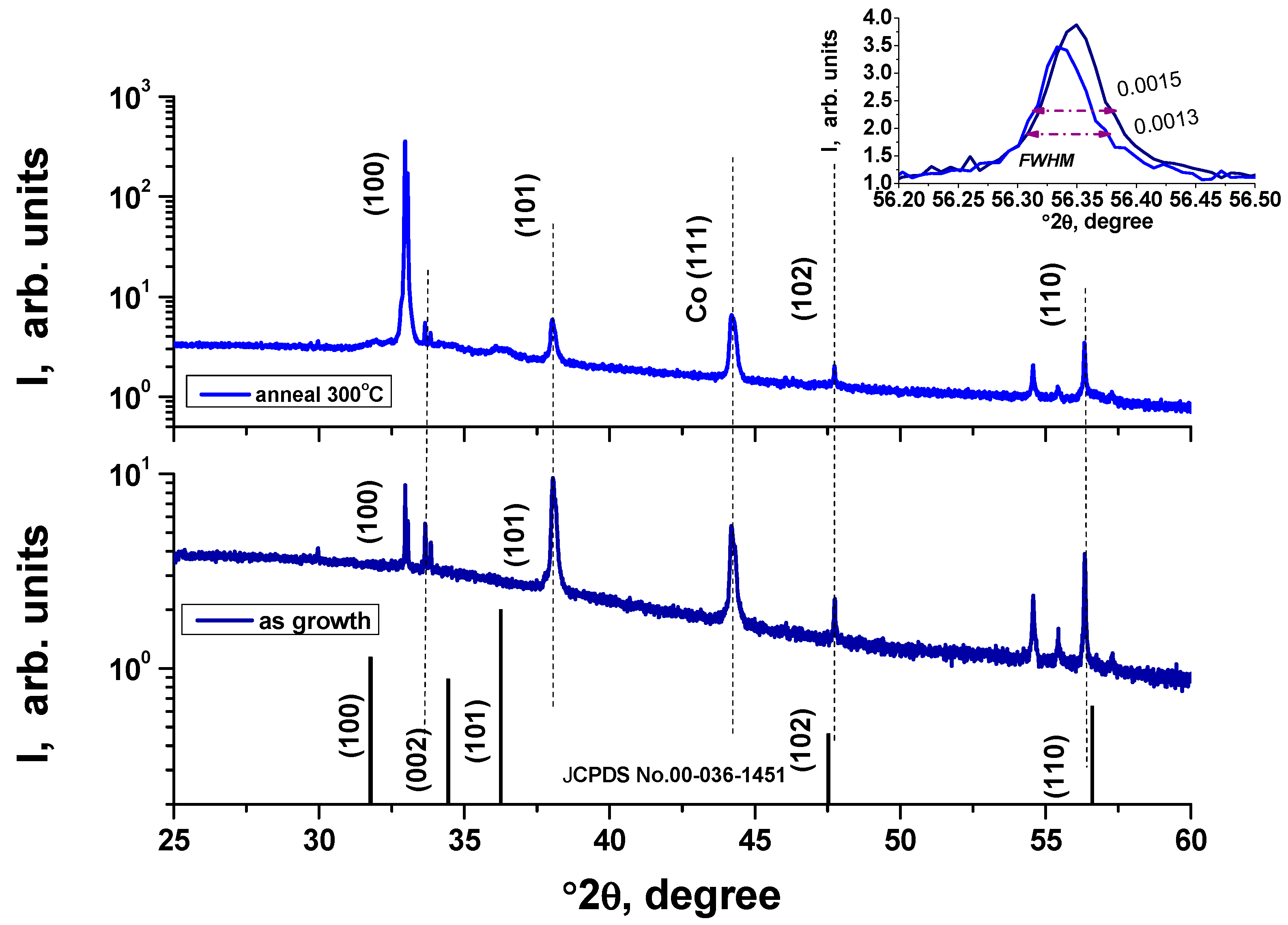
3.1. The Crystal Structure

X-ray diffractograms of the ZnO:Co nanostructured layers are shown in Figure 1. All layers show polycrystalline structures. The observed reflections come from hexagonal ZnO wurtzite P63mc group (JCPDS No. 00-89-0510). A strong diffraction peak (100) at 34.40 °2θ indicates that the grain growth mechanism of the c-axis mainly parallel to the substrate surface along the crystallographic axis was observed [35,36]. Other pure reflections (101), (102), (110), (103), and (112) corresponding to the ZnO orientation planes are also visible. The peak near 44.4 °2θ comes from cobalt (111) JCPDS No. 00-001-1259. The peaks around 55 °2θ are from impurities in the substrate, such as barium, which is a standard additive that increases acceptor conductivity in silicon substrates. Decreases in the value of the interplanar distance d (from the well-known Bragg’s law [37]) leads to the observation of a shift of the peak (100) toward the higher 2θ values. We observe a shift of the reflections towards higher values of 2θ, which was also observed for ZnO layers with a 3% concentration of Co ions by Shunmuga Sundaram et al. [38]. Thus, this indicates that the applied growth technique is effective in generating uncontaminated ZnO layers.
The texture of a certain plane is represented by the factor F. The degree of crystalline orientation can be determined from the XRD patterns using the Lotgering F factor (Equation (1)), given as follows:
F = p p 0 1 p 0
p 0 = I 0 ( h 00 )   I 0 ( h k l )
p = I ( h 00 )   I ( h k l )
where I(hkl) and I0(hkl) are the intensity of the XRD peaks for the sample and reference. The parameters p and p0 represent the relative contribution of the reflections (h00) to the sum of all the reflections for the sample and reference. If F ≈ 1, it corresponds to the desired height. The F values were calculated for the first three major peaks. The degree of crystalline orientation to the plane (100) increases from F = 0.08 (before annealing) to F = 0.94 (after annealing at 400 °C). All ZnO:Co layers showed an increased intensity in the diffraction pattern corresponding to the reflection of (100) compared to (002) and (101). This indicated a dominant orientation along the axis ϕ, which was related to the minimum value of surface free energy (100). The crystallite size D of the ZnO:Co layers was determined from the FWHM, for the first three peaks, using the well-known Scherrer equation D = 0.9λ/(β·cosθ), where β = FWHM. The equation gave an estimate of the grain size D = 110 ÷ 140 nm. An increase in grain size of 27% and a change in orientation during annealing at 300 °C were observed. Zhang et al. observed a similar effect [39]. The annealing temperature has little influence on the grain size (which was also observed for pure ZnO layers [40]). In addition, changing the temperature of the substrate has a very strong effect on the quality of the resulting layer [36]. The layers had a predominantly a-axis oriented phase. At high concentrations of cobalt ions, precipitation of cobalt metal appears (corresponding to the peak near 44.4 °2θ).

3.2. Optical Measurements

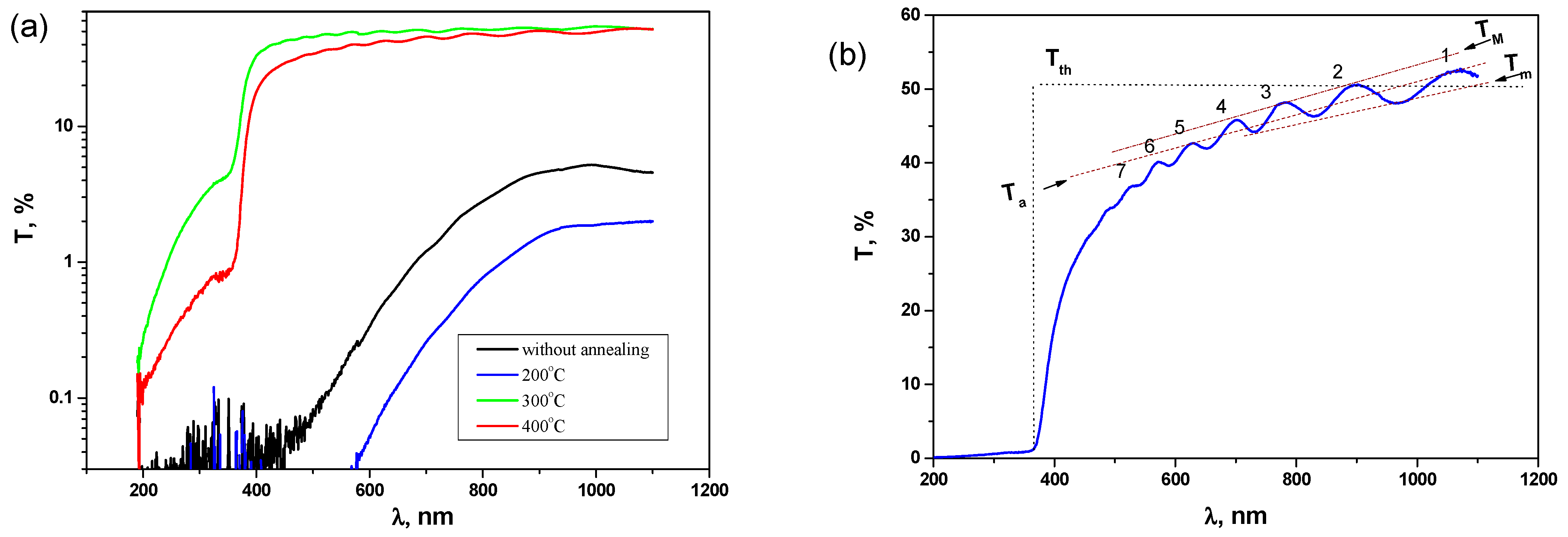
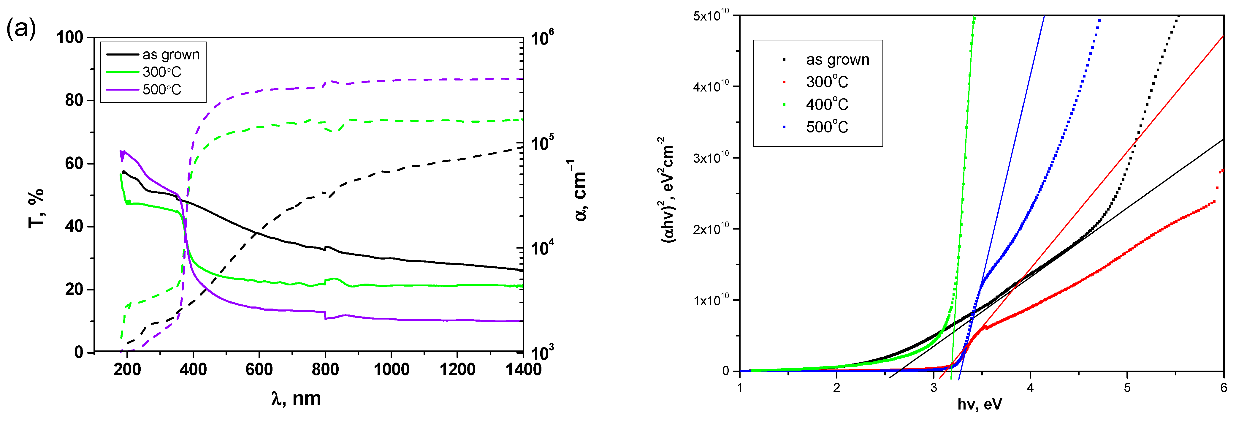
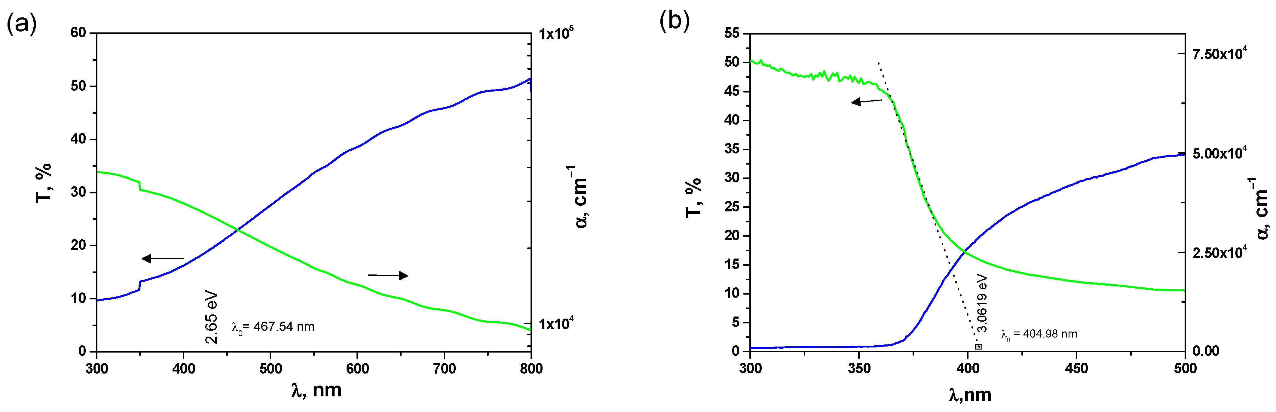
3.2.1. Transmission Spectra

The transmission curves for thin layers of cobalt-doped ZnO at different annealed temperatures are shown in Figure 2a.
The non-annealed layer shows low optical transmission, with very low transmission in the region below 600 nm due to the presence of cobalt ions [41]. The increase in transmission after annealing at 300 °C and 400 °C, compared to the non-annealed layer, is due to a reduction in the amount of oxygen vacancies in the layer [33]. The excellent surface quality and uniformity of the layers is confirmed by the appearance of interference bands in the transmission spectra (Figure 2b), which occurs when the surface of the layer reflects light without much scattering/absorption over most of the layer area. The number of interference fringes observed on the curve is limited to eight maxima only because of the relatively small thickness of the sample (1000 nm). As the thickness of the layers increases, the number of interference fringes increases. It is worth mentioning that the ZnO:Co samples prepared and annealed in this way are thin and homogeneous. This was confirmed by the appearance of regular interference peaks in the measured transmission spectra of the layers. In the area of shorter wavelengths (λ < 500 nm), transmission increases sharply with increasing wavelength, most likely due to the influence of the absorption edge. The increase in the annealing temperature leads to a transmission threshold shift to shorter wavelengths (in Figure 2a). This shift of the band-gap optical width toward higher energy may be associated with better structural order, residual stress removal, and quantum constraint effects.
To increase the crystalline character of the layers, they were annealed, which led to an increase in the size of the crystallites. Changing the annealing temperature weakly affects the degree of crystallinity. On the other hand, the transmission of the sample without annealing has the lowest values (black line in Figure 2a), which means that this sample has the highest refractive index. The transmission of the sample annealed at 300 °C has the highest values, which corresponds to the lowest refractive index among the samples.

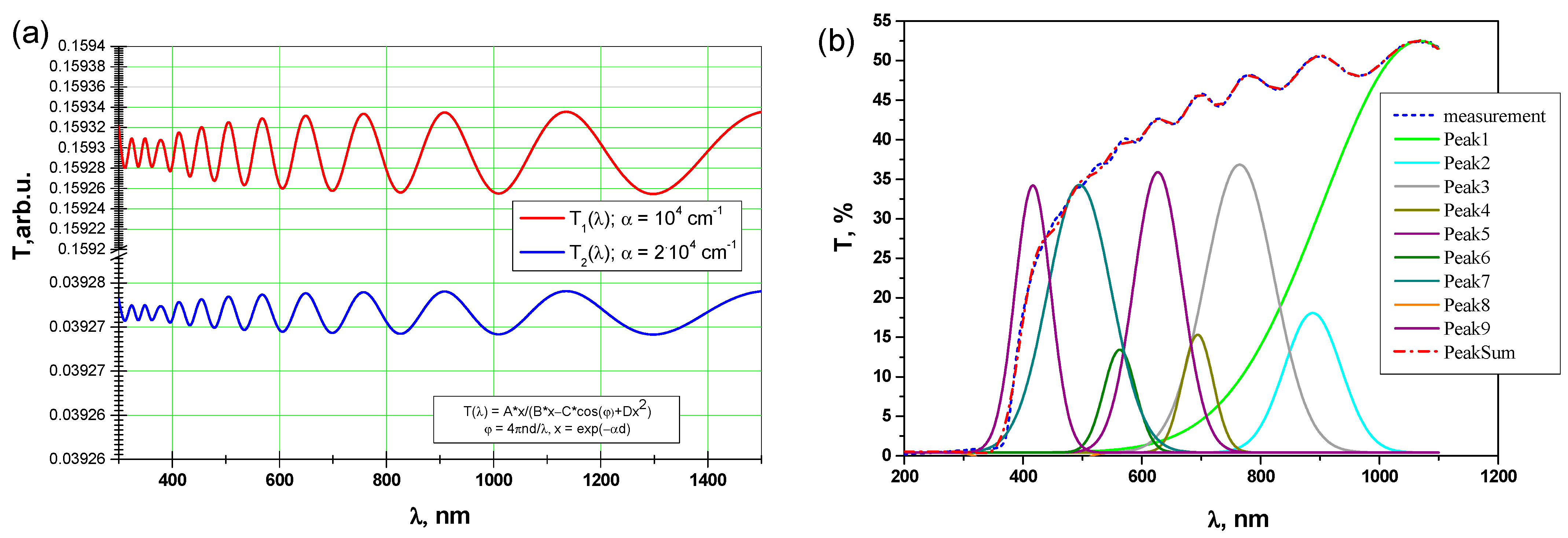
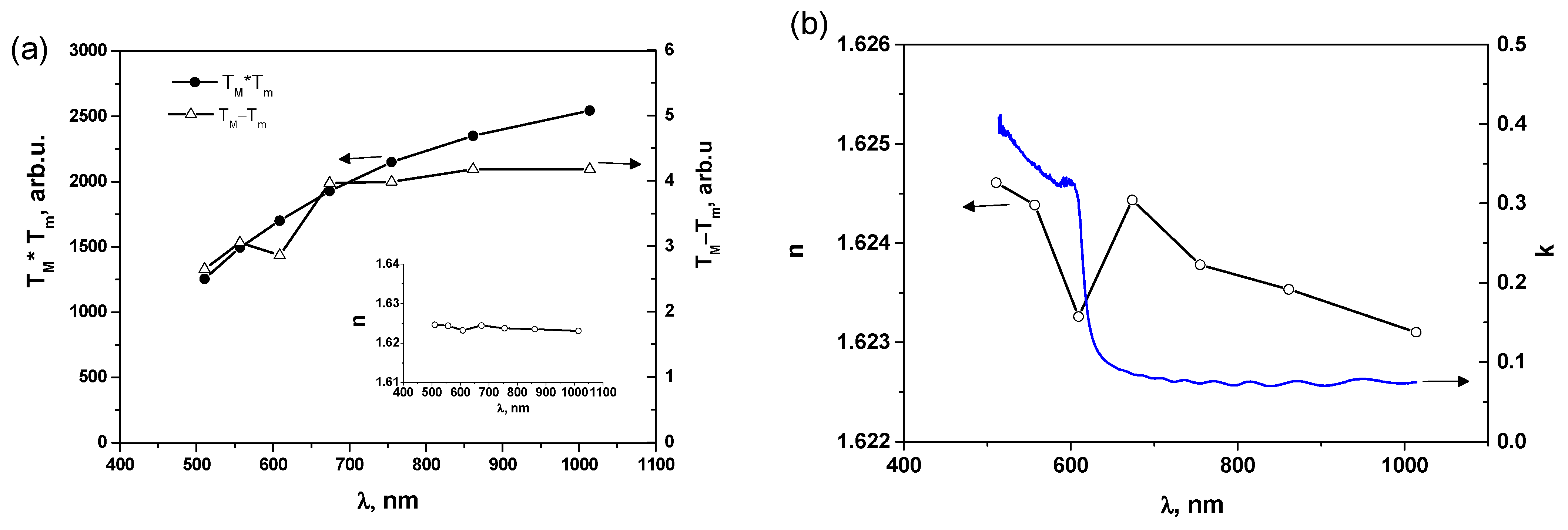
3.2.2. Refractive Index and Thickness

Assuming that the layer absorbs poorly and the substrate is completely transparent, the refractive index n and the light extinction coefficient k of the layers can be estimated from the transmission spectra using the envelope method [42,43]. A typical transmission spectrum T%(λ) of the ZnO:Co layer (annealed at 400 °C) with interference patterns is shown in Figure 2b. Three approximations are also shown: TM, Tm, and Ta for layers of ZnO:Co. The theoretical transmittance Tth is also illustrated. For comparison, the line Ta is an experimental approximation. The refractive index n is an important parameter for optical materials for optoelectronics applications [42,44]. From the curves TM(λ) and Tm(λ) of the layers in the spectral range of weak and medium absorption, the index n can be calculated using Equation (4):
n = N + ( N 2 n s 2 ) 1 / 2
N = 2 n s · T M T m T M · T m + n s 2 + 1 2
n s = 1 T S + 1 T S 2 1
where TM and Tm—the maximum and minimum transmission at a given wavelength, respectively; Ts—the transmission of the substrate; ns—the refractive index of the substrate (ns = 1.62).
The layer thickness d can be calculated from the equation:
d = λ 1 · λ 2 2 ( λ 1 n 2 λ 2 n 1 )
where λ1 and λ2—wavelengths corresponding to successive interference maxima; n1 and n2—the corresponding refractive indexes. The thickness values are given in Table 1.
Practical modelled interferences for thin layers on a transparent substrate are shown in Figure 3a. The transparent substrate with the refractive index ns and the transmittance TS has a thickness of several orders of magnitude greater than d. If the layer thickness is homogeneous, the interference effects give rise to a spectrum, shown by the full curves. The thickness, refractive index, absorption index, and transmittance of the ZnO:Co layer were estimated. The transmittance spectrum has the description of the Swanepoel method to match the optical parameters [43,45,46]. The transmission T for normal incidence resulting from the interference of the wave transmitted from the interfaces can be written as:
T = T ( n , x ) = A x B C x c o s ( φ ) + D x 2
where the matching parameters are: A = 68, B = 106, C = 0.11, D = −0.24, φ = 4πnd/λ, x = exp(-αd), and α = 4 πκ/λ. The curves for d = 1500 nm were adjusted for the two parameter values α = 104 cm−1 and α = 2 × 104 cm−1. For a thin layer on a non-absorbent substrate, the optical transmission of T for normal incidence is determined by the Swanepoel equations. Parameters n and k are the real and imaginary parts of the refractive index of the thickness of the thin layer, d is the thickness of the layer, and ns is the actual refractive index of the substrate (Equation (3)) [47,48]. The computational work was carried out on a simple theoretical model built on the basis of this algorithm. The substrate refractive index and the n and k values are calculated from the equations. Using the estimation, we can obtain the theoretical value of the transmittance, and, then, by appropriately evaluating the various predicted values of thickness d, we can calculate the exact thickness of the layer. The interference fringes can be used to calculate the optical constants of the layer [49]. The Gaussian distribution can model maxima of the fringes. The width of the peaks increases towards the longer wavelengths (Figure 3b).
The calculated dependence of the refractive index as a function of wavelength for the ZnO:Co layer annealed at 400 °C is shown in Figure 4a. It is clear that the refractive index n is close to 1.62 in the visible near infrared region and decreases with increasing wavelength. A similar trend is observed in the undoped ZnO layers [50]. This behavior can be explained by an increase in transmission and a decrease in the absorption coefficient with wavelength [51]. The behavior of the refractive index in the UV-VIS region is not uniform with wavelength because of the absorption of electrons that takes place (Figure 4b), where the lowest value of the refractive index is observed at 590 nm.
In the visible and near-infrared regions, the refractive index decreases with wavelength, indicating normal dispersion. The calculated refractive index at λ= 700 nm for the ZnO:Co layer annealed at 400 °C is 1.624 (Figure 4b). It is less than the basic value for the stoichiometric ZnO obtained by the sputter deposition method [52]. This can be explained by the low packing density of the layers obtained by the used PLD method. Whereas, Stelling et al. [53] showed that the refractive index for undoped ZnO layers for wavelengths above 800 nm was lower than 1.60. An increase in the refractive index with doping can be explained by changing the value of the polarization of the smaller atomic radius of Co [54]. This may be attributed to the small difference between the ionic diameters of the Co+2 (0.69 nm) and Zn+2 (0.74) [55,56]. A similar effect is seen in Si-doped ZnO [57]. Co2+ ions in the crystal structure of ZnO (presented in [58]) substitute the Zn2+ ions [55]. The decrease in transmission results from the presence of the absorption band located at λ ≈ 550 nm, which is caused by energy-to-energy transitions. The absorption arm is believed to be due to an electron transition to the dopant levels, and the increase in the absorption of the doped ZnO layers may be a result of the high reflectance. Moreover, at different concentrations of Co ions, the absorption coefficient changes slightly.
Changes in the refractive index n and the extinction coefficient k as a function of wavelengths in the range of 400–1000 nm are shown in Figure 4b. In the absorption area, the absorption coefficient of the layer and the extinction coefficient were calculated using the following equation:
α = 2.303 A d
k = α λ 4 π
where A—optical absorption constant (absorbance ln(I/I0)); d—thickness of the layers [59].
The parameters used for the calculation of the refractive index parameter are given in Table 2, and Tmax − Tmin and Tmax × Tmin are presented in Figure 4a.

3.2.3. Optical Zone

There is agreement between the obtained values of the thickness of the layer, both annealed and non-annealed, and those calculated by the Swanpoel method. Figure 5a shows the absorption spectrum calculated by Equation (9). Annealing of the ZnO:Co layer leads to a decrease in the value of the absorption coefficient. Figure 5b show the plot (α·hν)2 versus for thin ZnO:Co layers. The plot is linear over a wide range of photon energies, indicating a simple type of transition. The intersections of the extrapolation of these sections (straight lines) with the energy axis reflect the width of the optical band gap. The optical absorption edge was analyzed using Equation (11), described by the directly allowed transition [33]:
α h ν = B ( h ν E g ) 1 / 2
where B—band edge sharpness is a constant and it was obtained from the slope of the plot in the range of interband absorption [48]; Eg—optical energy gap.
We point out that the increase in the degree of crystallinity of the layer after annealing leads to a change in the shape of the fundamental absorption edge.
The calculated values of the optical band gap are, respectively, 2.63 eV (for as grown), 3.11 eV (annealed at 300 °C), 3.15 eV (annealed at 400 °C), and 3.28 eV (annealed at 500 °C). The obtained values of the optical band gap of ZnO:Co (Figure 5b) are smaller than for pure ZnO (about 3.37 eV), which is consistent with observations made in the works [41,60]. The decrease in the value of the optical band gap can be resulted from active transitions involving 3d levels of Co2+ ions and intense sp-d interactions between itinerant ‘sp’ carriers and localized ‘d’ dopant electrons [41].
Table 3 shows that the value of the ZnO:Co optical band gap depends on the cobalt content, as well as the annealing temperature in post-growth.

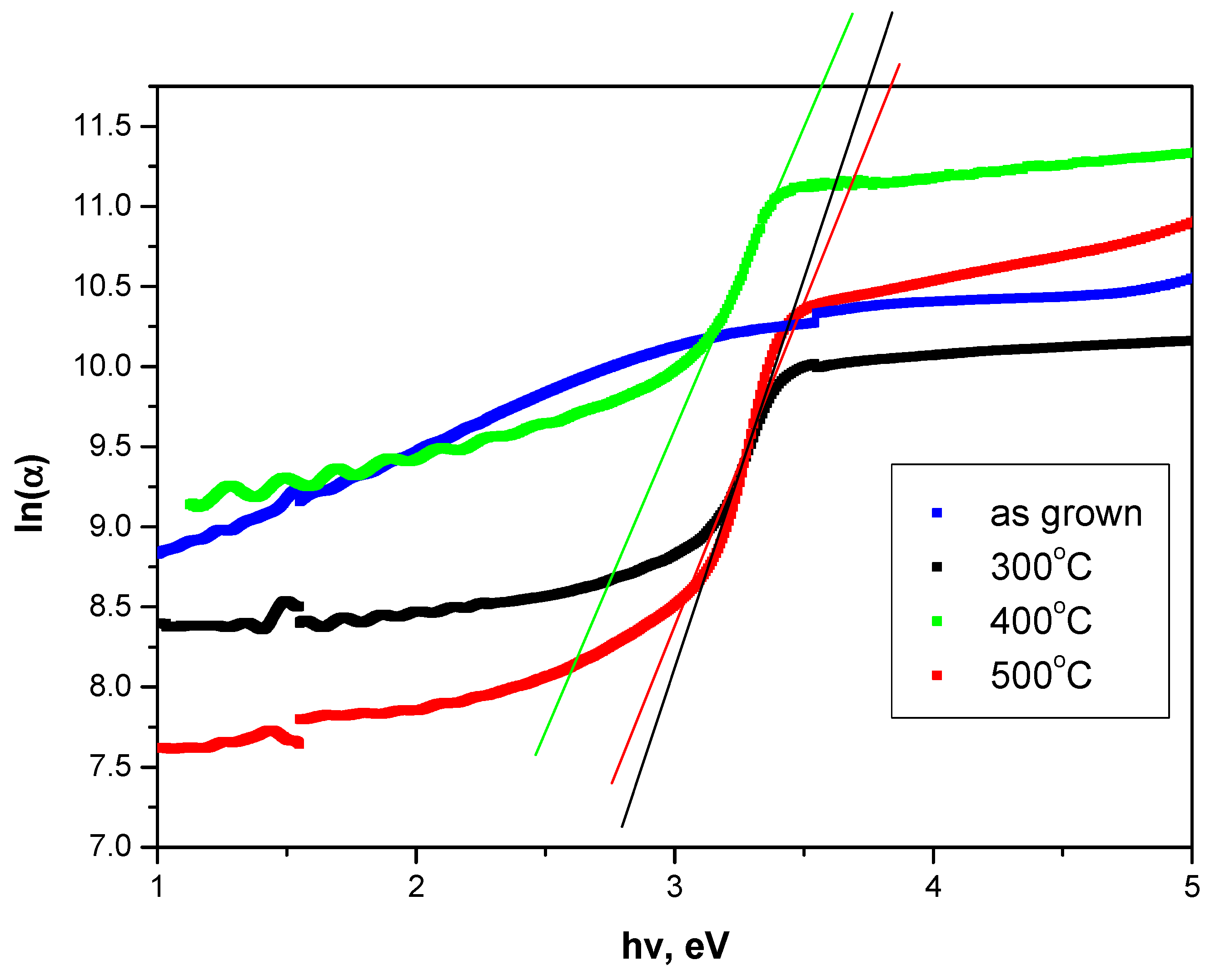
3.2.4. Calculations of the Shape of the Urbach Absorption Edge

As already mentioned, the values of Eg for the ZnO:Co layers were calculated. As can be seen in Figure 5b, for example, nanostructured ZnO:Co layers (annealed at 400 °C) have a shift in the position of the optical band gap from 3.37 to 3.15 eV, relating to pure ZnO [66,67,68]. This shift can be explained by the development of the resonance structure in the density of states, and the splitting of the band by introducing deep states into the region of the band gap. Thus, it can be used to extend the optoelectronic and photoelectric applications of these layers. The Urbach energy EU is related to the width of the exponential edge of the absorption (tail) and can be calculated using the following equation:
E U = α 0 · e x p ( h ν E U ) 1 E U = [ d ( ln ( α ) ) d ( h ν ) ] 1
where α0—the parameter of the tail range that can be found in the dependencies:
α 0 = 2 σ 0 ( 4 π c ) Δ E
where σo—the electrical conductivity at a temperature of absolute zero; c—the speed of light; ΔE—the tail width of the localized band gap states [69]. EU values were obtained from the slopes of the linear part of the curve ln (α) with respect to (Figure 6). The EU value, for the annealed layers, increases with annealing temperature from 200 meV (at a temperature of 300 °C) to 250 meV (at a temperature of 400 °C). This corresponds to the transition from the morphology of the hexagonal nanodisks to nanowires against the hexagonal morphology of the nanodisks. The increase in the value of the EU can be explained by a violation of the structure of the material, which leads to the formation of a tail in the valence and conductivity zones. These results are confirmed by XRD measurements, in which the crystallite planes of the ZnO:Co layers show the lowest preferred orientation along the α-axis direction (100) compared to other ZnO layers.
Experimental results concerning the change of the optical gap of the thin layer and disturbances (Urbach energy given for each sample) depending on the annealing are presented in Figure 6. The presence of high concentrations of states located in thin layers causes the reduction of the optical width of the band gap. Therefore, the addition of Co ions increases the concentration of states, which reduces the band gap. Although the Tauc method is based on the application of a linear approximation to the major absorption edge in the band-gap width, the effect of lower energy states on defect absorption may affect the accuracy of the band-gap determination [70,71]. This deviation from linearity in the low-energy field is often referred to as the Urbach tail. The oscillator model [72] is based on a certain dependence of the refractive index dispersion below the interband absorption limit: the dispersion energy. It is an indicator of the intensity of the interband optical transition. In the Urbach–Martienssen model, the Urbach energy EU is the main parameter that determines the photon capture efficiency of a semiconductor layer. Point-defective binary semiconductor compounds have a special optical absorption edge profile. The absorption coefficient increases exponentially with the energy of the photons near the band gap [73].
The layer is formed by the plasma deposition from the target [74,75]. The obtained material contains various types of impurities that cause disturbances in the crystal structure. The crystal lattice limiting the pure EV and EC zones may disappear. When the perturbation becomes too high (for example, due to the appearance of impurities in the material), the tails may overlap. To define this disorder, we use the Urbach parameter EU. After examining the changes in the absorption coefficient, it is possible to estimate the existing disturbance in the layers. The exponential dependence of the photon energy on the absorption coefficient α at the edge of the band for noncrystalline materials corresponds to the Urbach ratio Equation (12). The Urbach curve shows the change in the logarithm of the absorption coefficient as a function of the photon energy for the layer [76]. The value of Urbach energy (EU) is usually calculated taking into account the inverse value of the slope of the linear portion in the lower photon energy region of these curves. The calculated Urbach energy values for the annealed ZnO:Co layer are about 200 meV. The Urbach energy value is derived from the plot (lnα) as a function of . Urbach’s energy depends on soaking in. Increasing the annealing temperature of the ZnO:Co layer increases the EC from 200 to 250 meV. This result shows the difference in the type of incorporation of growth defects in the ZnO matrix. Moreover, there is a strong correlation with the Urbach energy when the difference in the ion radii between the zinc and alloying elements and the difference in the degree of oxidation.
This confirms the inclusion of these absorbing defects in the ZnO matrix, which introduces certain perturbations in the energy zones [77]. The result is also confirmed by the structural studies described above. The Urbach tail in the optical absorption of doped ZnO thin layers may occur because of the expansion of defect levels due to their spatial overlap in the conductivity band and nonuniform defect distribution.

3.2.5. Quantitative Assessment of the Effects of Urbach Tail

The calculated optical band gap for the layers is smaller than for the pure ZnO (3.37 eV). The reduction in the value of the optical band gap can be attributed to the location of the Co3p states in the ZnO layer above the top of the valence band and in combination with the O2p states, leading to a narrowing of the gap. To estimate the characteristics of ZnO:Co near the conduction band, the absorption behavior at lower photon energy is interpreted by Urbach’s rule: α = K.exp (E/EU), where K is constant and EU is Urbach energy, which is interpreted as the formation of localized tails in the width of the gap. This region results from the transitions between states stretched in one band and states located in the exponential tail of the other, and as a consequence of all defects. It was observed that the increase in layer thickness leads to an increase in the value of dispersion energy.
The presence of high concentrations of states located in thin layers causes the optical gap width to be reduced. Therefore, the addition of Co ions increases the concentration of states located in the layer, which reduces the band gap. The inclusion of Urbach endpoints in the linear selection method may reduce the resulting extrapolated gap width, and, therefore, also reduces the corresponding value of the slope. The plot showing the absorption of the Urbach tail, which can usually be described by an exponential function, is shown in Figure 7.
To determine the size of Urbach tail in the graph, we introduced a value called the edge absorption coefficient (NEAR). In a perfect material that has absolutely no Urbach tail, the value (αhν)2 will be zero with respect to the optical gap. Yet, there is always additional absorption in real materials. To estimate this, we compare the value (αhν)2 at the extrapolated optical gap width with a value taken at slightly higher energy, where most of the signal will come from the band transition. The square root of this ratio is then taken into account to further extend the NEAR concept to potential applications in indirect absorbent materials. If the Urbach tail is significant, the NEAR will approach one. If the material is without defects, the NEAR value will be small (ideally approaching 0). In the following, the NEAR value (Figure 7) for each of the plots was calculated. This way, we were able to examine how precise the Tauc slope values were and whether the precision decreased with more flawed material:
N E A R = 1.02 · ( α h ν ) 2 | h ν = E g ( α h ν ) 2 | h ν = 1.02 E g = α ( E g ) α ( 1.02 · E g )
The following results were obtained from Equation (13) for ZnO:Co layers annealed at different temperatures: NEAR = 0.98 (as growth) and NEAR = 0.91 (annealed in 400 °C).

4. Conclusions

Thin layers of cobalt-doped ZnO were applied by the PLD method on a different substrates. The cobalt content in the initial solution was 20% at. The absorption changes after annealing the sample and for the studied layers is in the range of 103–105 cm−1. The small value of the extinction coefficient determined for the annealed sample (less than 0.4) indicates a good optical quality of the obtained layer. The achieved optical band gap corresponds to straight transitions and is smaller (2.65 eV for the non-annealed layer) than for pure ZnO. Annealing leads to an increase in the optical band gap. In addition, cobalt doping changes the value of the refractive index. Crystallinity and grain size be improved with annealing, but the annealing temperature (200–500 °C) has no significant effect here.
The Urbach EU parameter was used to determine the inhomogeneity of the crystal structure of the layers. Changes in the absorption coefficient were studied and existing perturbations were evaluated. The Urbach curve shows the change in the logarithm of the absorption coefficient as a function of the photon energy for the layers. The calculated values of the Urbach energy for the ZnO:Co layer were about 0.20 eV. Increasing the annealing temperature of the ZnO:Co layers increased the parameter EU from 0.20 (for 300 °C) to 0.25 eV (for 400 °C), which showed the difference in the type of growth defects in the ZnO matrix. We have shown that the shape of the fundamental absorption edge can be modified by temperature treatment of the material.

Supplementary Materials

The following are available online at https://www.mdpi.com/article/10.3390/app13042701/s1, Figure S1: Temperature dependence of resistance for ZnO:Co layers annealed at two temperatures (250 °C and 300 °C), Figure S2: SEM image of the ZnO:Co layer annealed in temperature 300 °C, Figure S3: EDS analysis of the ZnO:Co, Table S1: EDS analysis of ZnO:Co.

Author Contributions

Conceptualization, P.P. and I.S.V.; methodology, P.P., I.S.V. and B.C.; investigation, P.P., I.S.V. and B.C.; data curation, P.P., I.S.V. and B.C.; writing—original draft preparation, P.P. and B.C.; writing—review and editing, P.P., I.S.V. and B.C. All authors have read and agreed to the published version of the manuscript.

Funding

This research received no external funding.

Institutional Review Board Statement

Not applicable.

Informed Consent Statement

Not applicable.

Data Availability Statement

Data available in a publicly accessible repository.

Conflicts of Interest

The authors declare no conflict of interest.

References

  1. Klingshirn, C.F.; Meyer, B.K.; Waag, A.; Hoffmann, A.; Geurts, J. Zinc Oxide—From Fundamental Properties Towards Novel Applications; Springer: Berlin/Heidelberg, Germany, 2010; ISBN 978-3-642-10576-0. [Google Scholar]
  2. Korotcenkov, G. Nanostructured Zinc Oxide: Synthesis, Properties and Applications; Awasthi, K., Ed.; Metal Oxid.; Elsevier: Amsterdam, The Netherlands, 2021; ISBN 9780128189009. [Google Scholar]
  3. Witkowski, B.S. Applications of ZnO Nanorods and Nanowires—A Review. Acta Phys. Pol. A 2018, 134, 1226–1246. [Google Scholar] [CrossRef]
  4. Xiao, Y. Application Analysis of Zinc Oxide Nanomaterials Based on Quantum Dots in Energy Environment. J. Phys. Conf. Ser. 2021, 1748, 52011. [Google Scholar] [CrossRef]
  5. Özgür, Ü.; Hofstetter, D.; Morkoç, H. ZnO Devices and Applications: A Review of Current Status and Future Prospects. Proc. IEEE 2010, 98, 1255–1268. [Google Scholar] [CrossRef]
  6. Aleksanyan, M.; Sayunts, A.; Aroutiounian, V.; Shahkhatuni, G.; Simonyan, Z.; Shahnazaryan, G. Gas Sensor Based on ZnO Nanostructured Film for the Detection of Ethanol Vapor. Chemosensors 2022, 10, 245. [Google Scholar] [CrossRef]
  7. Chen, Z.; Wang, J.; Wu, H.; Yang, J.; Wang, Y.; Zhang, J.; Bao, Q.; Wang, M.; Ma, Z.; Tress, W.; et al. A Transparent Electrode Based on Solution-Processed ZnO for Organic Optoelectronic Devices. Nat. Commun. 2022, 13, 4387. [Google Scholar] [CrossRef]
  8. Djurišić, A.B.; Ng, A.M.C.; Chen, X.Y. ZnO nanostructures for optoelectronics: Material properties and device applications. Prog. Quantum. Electron. 2010, 34, 191–259. [Google Scholar] [CrossRef]
  9. Ding, M.; Guo, Z.; Zhou, L.; Fang, X.; Zhang, L.; Zeng, L.; Xie, L.; Zhao, H. One-Dimensional Zinc Oxide Nanomaterials for Application in High-Performance Advanced Optoelectronic Devices. Crystals 2018, 8, 223. [Google Scholar] [CrossRef] [Green Version]
  10. Zahoor, R.; Jalil, A.; Ilyas, S.Z.; Ahmed, S.; Hassan, A. Optoelectronic and solar cell applications of ZnO nanostructures. Results Surf. Interfaces 2021, 2, 100003. [Google Scholar] [CrossRef]
  11. Safa, S.; Nejad, A.M. Influence of Cr dopant on the microstructure and optical properties of ZnO nanorods. J. Adv. Mater. Process. 2014, 2, 19–24. [Google Scholar]
  12. Stehr, J.; Buyanova, I.; Chen, W. Defects in Advanced Electronic Materials and Novel Low Dimensional Structures; Stehr, J., Buyanova, I., Chen, W., Eds.; Elsevier: Amsterdam, The Netherlands, 2018; ISBN 978-0-08-102053-1. [Google Scholar]
  13. Ayoub, I.; Kumar, V.; Abolhassani, R.; Sehgal, R.; Sharma, V.; Sehgal, R.; Swart, H.C.; Mishra, Y.K. Advances in ZnO: Manipulation of defects for enhancing their technological potentials. Nanotechnol. Rev. 2022, 11, 575–619. [Google Scholar] [CrossRef]
  14. Janotti, A.; Van De Walle, C.G. Fundamentals of zinc oxide as a semiconductor. Rep. Prog. Phys. 2009, 72, 126501. [Google Scholar] [CrossRef] [Green Version]
  15. Yang, A.; Yang, Y.; Zhang, Z.; Bao, X.; Yang, R.; Li, S.; Sun, L. Photoluminescence and defect evolution of nano-ZnO thin films at low temperature annealing. Sci. China Technol. Sci. 2013, 56, 25–31. [Google Scholar] [CrossRef]
  16. Djurišić, A.B.; Leung, Y.H. Optical Properties of ZnO Nanostructures. Small 2006, 2, 944–961. [Google Scholar] [CrossRef] [PubMed]
  17. Xu, P.S.; Sun, Y.M.; Shi, C.S.; Xu, F.Q.; Pan, H.B. The electronic structure and spectral properties of ZnO and its defects. Nucl. Instrum. Methods Phys. Res. Sect. B Beam Interact. Mater. Atoms 2003, 199, 286–290. [Google Scholar] [CrossRef]
  18. Kittilstved, K.R.; Liu, W.K.; Gamelin, D.R. Electronic structure origins of polarity-dependent high-Tc ferromagnetism in oxide-diluted magnetic semiconductors. Nat. Mater. 2006, 5, 291–297. [Google Scholar] [CrossRef] [PubMed]
  19. Li, M.; Xu, J.; Chen, X.; Zhang, X.; Wu, Y.; Li, P.; Niu, X.; Luo, C.; Li, L. Structural and optical properties of cobalt doped ZnO nanocrystals. Superlattices Microstruct. 2012, 52, 824–833. [Google Scholar] [CrossRef]
  20. Dietl, T.; Ohno, H.; Matsukura, F.; Cibert, J.; Ferrand, D. Zener Model Description of Ferromagnetism in Zinc-Blende Magnetic Semiconductors. Science 2000, 287, 1019–1022. [Google Scholar] [CrossRef] [PubMed] [Green Version]
  21. Cieniek, B.; Stefaniuk, I.; Virt, I.; Gamernyk, R.V.; Rogalska, I. Zinc–Cobalt Oxide Thin Films: High Curie Temperature Studied by Electron Magnetic Resonance. Molecules 2022, 27, 8500. [Google Scholar] [CrossRef]
  22. Mukhtar, M.; Munisa, L.; Saleh, R. Co-Precipitation Synthesis and Characterization of Nanocrystalline Zinc Oxide Particles Doped with Cu2+ Ions. Mater. Sci. Appl. 2012, 3, 543–551. [Google Scholar] [CrossRef] [Green Version]
  23. El-Hilo, M.; Dakhel, A.A.; Ali-Mohamed, A.Y. Room temperature ferromagnetism in nanocrystalline Ni-doped ZnO synthesized by co-precipitation. J. Magn. Magn. Mater. 2009, 321, 2279–2283. [Google Scholar] [CrossRef]
  24. Zhang, F.; Yuan, X.; Fu, D.; Zhou, L.; Huang, P.; Chen, T. Co-doped zinc oxide microspheres as photocatalysts for enhanced uranium extraction. J. Radioanal. Nucl. Chem. 2023, 332, 289–296. [Google Scholar] [CrossRef]
  25. Yang, A.; Hou, Q.; Yin, X.; Qi, M.; Wang, Z. First principles study on p-type conductivity and new magnetic mechanism of ZnO:Sm with point defects in different strains. Solid State Commun. 2022, 348–349, 114738. [Google Scholar] [CrossRef]
  26. Vegesna, S.V.; Bhat, V.J.; Bürger, D.; Dellith, J.; Skorupa, I.; Schmidt, O.G.; Schmidt, H. Increased static dielectric constant in ZnMnO and ZnCoO thin films with bound magnetic polarons. Sci. Rep. 2020, 10, 6698. [Google Scholar] [CrossRef] [Green Version]
  27. Ciolan, M.A.; Motrescu, I. Pulsed Laser Ablation: A Facile and Low-Temperature Fabrication of Highly Oriented n-Type Zinc Oxide Thin Films. Appl. Sci. 2022, 12, 917. [Google Scholar] [CrossRef]
  28. Zeng, W.; Wang, Z.; Fasquelle, D.; Députier, S.; Bouquet, V.; Guilloux-Viry, M. Effect of the Microstructure of ZnO Thin Films Prepared by PLD on Their Performance as Toxic Gas Sensors. Chemosens 2022, 10, 285. [Google Scholar] [CrossRef]
  29. Haider, A.J.; Jabbar, A.A.; Ali, G.A. A review of Pure and Doped ZnO Nanostructure Production and its Optical Properties Using Pulsed Laser Deposition Technique. J. Phys. Conf. Ser. 2021, 1795, 12015. [Google Scholar] [CrossRef]
  30. Tortosa, M.; Mollar, M.; Marí, B.; Lloret, F. Optical and magnetic properties of ZnCoO thin films synthesized by electrodeposition. J. Appl. Phys. 2008, 104, 33901. [Google Scholar] [CrossRef] [Green Version]
  31. Cieniek, B.; Stefaniuk, I.; Virt, I. EMR spectra thin films doped with high concentration of Co and Cr on quartz and sapphire substrates. Acta Phys. Pol. A 2017, 132, 30–33. [Google Scholar] [CrossRef]
  32. Cieniek, B.; Stefaniuk, I.; Virt, I. EPR study of ZnO:Co thin films grown by the PLD method. Nukleonika 2013, 58, 359–363. [Google Scholar]
  33. Wisz, G.; Virt, I.; Sagan, P.; Potera, P.; Yavorskyi, R. Structural, Optical and Electrical Properties of Zinc Oxide Layers Produced by Pulsed Laser Deposition Method. Nanoscale Res. Lett. 2017, 12, 253. [Google Scholar] [CrossRef] [Green Version]
  34. Virt, I.; Hadzaman, I.V.; Bilyk, I.S.; Rudyi, I.O.; Kurilo, I.V.; Frugynskyi, M.S.; Potera, P. Properties of ZnO and ZnMnO Thin Films Obtained by Pulsed Laser Ablation. Acta Phys. Pol. A 2010, 117, 34–37. [Google Scholar] [CrossRef]
  35. Seetawan, U.; Jugsujinda, S.; Seetawan, T.; Ratchasin, A.; Euvananont, C.; Junin, C.; Thanachayanont, C.; Chainaronk, P. Effect of Calcinations Temperature on Crystallography and Nanoparticles in ZnO Disk. Mater. Sci. Appl. 2011, 2, 1302–1306. [Google Scholar] [CrossRef] [Green Version]
  36. Chau, J.L.H.; Yang, M.C.; Nakamura, T.; Sato, S.; Yang, C.C.; Cheng, C.W. Fabrication of ZnO thin films by femtosecond pulsed laser deposition. Opt. Laser Technol. 2010, 42, 1337–1339. [Google Scholar] [CrossRef]
  37. Cullity, B.D.; Weymouth, J.W. Elements of X-Ray Diffraction. Am. J. Phys. 1957, 25, 394–395. [Google Scholar] [CrossRef] [Green Version]
  38. Shunmuga Sundaram, P.; Sangeetha, T.; Rajakarthihan, S.; Vijayalaksmi, R.; Elangovan, A.; Arivazhagan, G. XRD structural studies on cobalt doped zinc oxide nanoparticles synthesized by coprecipitation method: Williamson-Hall and size-strain plot approaches. Phys. B Condens. Matter 2020, 595, 412342. [Google Scholar] [CrossRef]
  39. Zhang, D.; He, Y.; Wang, C.Z. Structure and optical properties of nanostructured zinc oxide films with different growth temperatures. Opt. Laser Technol. 2010, 42, 556–560. [Google Scholar] [CrossRef]
  40. Saleem, M.; Fang, L.; Huang, Q.L.; Li, D.C.; Wu, F.; Ruan, H.B.; Kong, C.Y. Annealing Treatment Of Zno Thin Films Deposited By Sol–Gel Method. Surf. Rev. Lett. 2012, 19, 1250055. [Google Scholar] [CrossRef]
  41. Roguai, S.; Djelloul, A. Roles of Cobalt Doping on Structural and Optical of ZnO Thin Films by Ultrasonic Spray Pyrolysis. In Thin Films; Ares, A.E., Ed.; IntechOpen: London, UK, 2021; ISBN 978-1-83881-993-4. [Google Scholar]
  42. Aydin, H.; Aydin, C.; Al-Ghamdi, A.A.; Farooq, W.A.; Yakuphanoglu, F. Refractive index dispersion properties of Cr-doped ZnO thin films by sol-gel spin coating method. Optik 2016, 127, 1879–1883. [Google Scholar] [CrossRef]
  43. Zhang, D.Y.; Wang, P.P.; Murakami, R.I.; Song, X.P. First-principles simulation and experimental evidence for improvement of transmittance in ZnO films. Prog. Nat. Sci. Mater. Int. 2011, 21, 40–45. [Google Scholar] [CrossRef] [Green Version]
  44. Narayanan, N.; Deepak, N.K. B-N codoped p type ZnO thin films for optoelectronic applications. Mater. Res. 2018, 21, 20170618. [Google Scholar] [CrossRef] [Green Version]
  45. Hassanien, A.S.; Aly, K.A.; Akl, A.A. Study of optical properties of thermally evaporated ZnSe thin films annealed at different pulsed laser powers. J. Alloys Compd. 2016, 685, 733–742. [Google Scholar] [CrossRef]
  46. Hussain, A.A.-K.; Aadim, K.A.; Slman, H.M. Structural and optical properties of ZnO doped Mg thin films deposited by pulse laser deposition (PLD). Iraqi J. Phys. 2019, 12, 56–61. [Google Scholar] [CrossRef]
  47. Wang, M.D.; Zhu, D.Y.; Liu, Y.; Zhang, L.; Zheng, C.X.; He, Z.H.; Chen, D.H.; Wen, L.S. Determination of thickness and optical constants of ZnO thin films prepared by filtered cathode vacuum arc deposition. Chin. Phys. Lett. 2008, 25, 743–746. [Google Scholar] [CrossRef]
  48. Bedia, A.; Bedia, F.Z.; Aillerie, M.; Maloufi, N.; Benyoucef, B. Influence of the Thickness on Optical Properties of Sprayed ZnO Hole-blocking Layers Dedicated to Inverted Organic Solar Cells. Energy Procedia 2014, 50, 603–609. [Google Scholar] [CrossRef]
  49. Müllerová, J.; Mudroň, J. Determination of optical parameters and thickness of thin films deposited on absorbing substrates using their reflection spectra. Acta Phys. Slovaca 2000, 50, 477–488. [Google Scholar]
  50. Gadallah, A.S.; El-Nahass, M.M. Structural, optical constants and photoluminescence of ZnO thin films grown by sol-gel spin coating. Adv. Condens. Matter Phys. 2013, 2013, 234546. [Google Scholar] [CrossRef] [Green Version]
  51. Xie, G.C.; Fanga, L.; Peng, L.P.; Liu, G.B.; Ruan, H.B.; Wu, F.; Kong, C.Y. Effect of In-doping on the Optical Constants of ZnO Thin Films. Phys. Procedia 2012, 32, 651–657. [Google Scholar] [CrossRef] [Green Version]
  52. Golaszewska, K.; Kamińska, E.; Pustelny, T.; Struk, P.; Piotrowski, T.; Piotrowska, A.; Ekielski, M.; Kruszka, R.; Wzorek, M.; Borysiewicz, M.; et al. Planar optical waveguides for application in optoelectronic gas sensors. Acta Phys. Pol. A 2008, 114, A-223–A-230. [Google Scholar] [CrossRef]
  53. Stelling, C.; Singh, C.R.; Karg, M.; König, T.A.F.; Thelakkat, M.; Retsch, M. Plasmonic nanomeshes: Their ambivalent role as transparent electrodes in organic solar cells. Sci. Rep. 2017, 7, 42530. [Google Scholar] [CrossRef] [PubMed] [Green Version]
  54. Kaphle, A.; Hari, P. Variation of index of refraction in cobalt doped ZnO nanostructures. J. Appl. Phys. 2017, 122, 165304. [Google Scholar] [CrossRef]
  55. Godavarti, U.; Mote, V.D.D.; Dasari, M. Role of cobalt doping on the electrical conductivity of ZnO nanoparticles. J. Asian Ceram. Soc. 2017, 5, 391–396. [Google Scholar] [CrossRef]
  56. Hassan, A.I.; Yahya, A.M. Structural and optical properties of NiO-ZnO nanocomposite thin film prepared by spray pyrolysis. In Proceedings of the AIP Conference Proceedings; AIP Publishing LLC: Long Island, NY, USA, 2020; Volume 2213, p. 20208. [Google Scholar]
  57. Sorar, I.; Saygin-Hinczewski, D.; Hinczewski, M.; Tepehan, F.Z. Optical and structural properties of Si-doped ZnO thin films. Appl. Surf. Sci. 2011, 257, 7343–7349. [Google Scholar] [CrossRef]
  58. Stefaniuk, I.; Cieniek, B.; Rogalska, I.; Virt, I.; Kościak, A. Magnetic properties of ZnO:Co layers obtained by pulsed laser deposition method. Mater. Sci. 2018, 36, 439–444. [Google Scholar] [CrossRef] [Green Version]
  59. Ilican, S.; Caglar, M.; Caglar, Y. Determination of the thickness and optical constants of transparent indium-doped ZnO thin films by the envelope method. Mater. Sci. Pol. 2007, 25, 709–718. [Google Scholar]
  60. Kumar, D.; Jat, S.K.; Khanna, P.K.; Vijayan, N.; Banerjee, S. Synthesis, characterization, and studies of PVA/Co-doped ZnO nanocomposite films. Int. J. Green Nanotechnol. Biomed. 2012, 4, 408–416. [Google Scholar] [CrossRef]
  61. Khlifi, N.; Ihzaz, N.; Mrabet, S.; Alyamani, A.; El Mir, L. X-ray peaks profile analysis, optical and cathodoluminescence investigations of cobalt-doped ZnO nanoparticles. J. Lumin. 2022, 245, 118770. [Google Scholar] [CrossRef]
  62. Kumar, Y.; Sahai, A.; Olive-Méndez, S.F.; Goswami, N.; Agarwal, V. Morphological transformations in cobalt doped zinc oxide nanostructures: Effect of doping concentration. Ceram. Int. 2016, 42, 5184–5194. [Google Scholar] [CrossRef]
  63. Benramache, S.; Benhaoua, B. Influence of substrate temperature and Cobalt concentration on structural and optical properties of ZnO thin films prepared by Ultrasonic spray technique. Superlattices Microstruct. 2012, 52, 807–815. [Google Scholar] [CrossRef]
  64. Kaphle, A.; Echeverria, E.; Mcllroy, D.N.; Roberts, K.; Hari, P. Thermo-Optical Properties of Cobalt-Doped Zinc Oxide (ZnO) Nanorods. J. Nanosci. Nanotechnol. 2019, 19, 3893–3904. [Google Scholar] [CrossRef]
  65. Kaphle, A.; Reed, T.; Apblett, A.; Hari, P. Doping efficiency in cobalt-doped ZnO nanostructured materials. J. Nanomater. 2019, 2019, 7034620. [Google Scholar] [CrossRef]
  66. Abirami, N.; Arulanantham, A.M.S.; Wilson, K.S.J.J. Structural and magnetic properties of cobalt doped ZnO thin films deposited by cost effective nebulizer spray pyrolysis technique. Mater. Res. Express 2020, 7, 26405. [Google Scholar] [CrossRef]
  67. Siagian, S.M.; Sutanto, H.; Permatasari, A. Effect of co doping to the optical properties of ZnO:Co Thin films deposited on glass substrate by sol-gel spray coating technique. J. Phys. Conf. Ser. 2017, 795, 12009. [Google Scholar] [CrossRef] [Green Version]
  68. Solati, E.; Dejam, L.; Dorranian, D. Effect of laser pulse energy and wavelength on the structure, morphology and optical properties of ZnO nanoparticles. Opt. Laser Technol. 2014, 58, 26–32. [Google Scholar] [CrossRef]
  69. Shaban, M.; Zayed, M.; Hamdy, H. Nanostructured ZnO thin films for self-cleaning applications. RSC Adv. 2017, 7, 617–631. [Google Scholar] [CrossRef]
  70. Coulter, J.B.; Birnie, D.P. Assessing Tauc Plot Slope Quantification: ZnO Thin Films as a Model System. Phys. Status Solidi Basic Res. 2018, 255, 1700393. [Google Scholar] [CrossRef]
  71. Viezbicke, B.D.; Patel, S.; Davis, B.E.; Birnie, D.P. Evaluation of the Tauc method for optical absorption edge determination: ZnO thin films as a model system. Phys. Status Solidi Basic Res. 2015, 252, 1700–1710. [Google Scholar] [CrossRef]
  72. Márquez, E.; Bernal-Oliva, A.M.; González-Leal, J.M.; Prieto-Alcón, R.; Ledesma, A.; Jiménez-Garay, R.; Mártil, I. Optical-constant calculation of non-uniform thickness thin films of the Ge10As15Se75 chalcogenide glassy alloy in the sub-band-gap region (0.1–1.8 eV). Mater. Chem. Phys. 1999, 60, 231–239. [Google Scholar] [CrossRef]
  73. Boukhachem, A.; Ouni, B.; Bouzidi, A.; Amlouk, A.; Boubaker, K.; Bouhafs, M.; Amlouk, M. Quantum Effects of Indium/Ytterbium Doping on ZnO-Like Nano-Condensed Matter in terms of Urbach-Martienssen and Wemple-DiDomenico Single-Oscillator Models Parameters. ISRN Condens. Matter Phys. 2012, 2012, 738023. [Google Scholar] [CrossRef] [Green Version]
  74. Quiñones-Galván, J.G.; Cardona, D.; Rivera, L.P.; Gómez-Rosas, G.; Chávez-Chávez, A. Effect of the copper plasma density on the growth of SiOx-Cu thin films by PLD. Mater. Lett. 2021, 284, 129024. [Google Scholar] [CrossRef]
  75. Escalona, M.; Bhuyan, H.; Valenzuela, J.C.; Ibacache, S.; Wyndham, E.; Favre, M.; Veloso, F.; Ruiz, H.M.; Wagenaars, E. Comparative study on the dynamics and the composition between a pulsed laser deposition (PLD) and a plasma enhanced PLD (PE-PLD). Results Phys. 2021, 24, 104066. [Google Scholar] [CrossRef]
  76. Saadi, H.; Rhouma, F.I.H.; Benzarti, Z.; Bougrioua, Z.; Guermazi, S.; Khirouni, K. Electrical conductivity improvement of Fe doped ZnO nanopowders. Mater. Res. Bull. 2020, 129, 110884. [Google Scholar] [CrossRef]
  77. Ismail, A.; Abdullah, M.J. The structural and optical properties of ZnO thin films prepared at different RF sputtering power. J. King Saud Univ. Sci. 2013, 25, 209–215. [Google Scholar] [CrossRef] [Green Version]
Figure 1. XRD diffractograms for thin layers of ZnO:Co grown in vacuum (on a silicon) at substrate temperature 30 °C, without annealing and annealed in air (at temperature 300 °C). JCPDS No. 00-036-1451 was also placed. In the inset, the peak width at half the maximum (FWHM) for the (110) peak is shown for both samples.
Applsci 13 02701 g001
Figure 2. (a) Optical transmission spectra of ZnO:Co layers at different annealing temperatures in air (in semi-logarithmic scale). The arrows show the transmission threshold shift to shorter wavelengths. (b) Transmission spectra of the ZnO:Co layer annealed at a temperature of 400 °C in air with interference patterns.
Applsci 13 02701 g002
Figure 3. (a) Modeling of interference fringes using the Swanepoel method. (b) Adjusting the interference fringes of optical transmission with Gauss.
Applsci 13 02701 g003
Figure 4. (a) Parameters of the optical transmission spectrum for the calculation of the refractive index n and the dependence of the refractive index on the wavelength for the ZnO:Co layer annealed at 400 °C, (b) Refractive index n (black line) and extinction coefficient k (blue line).
Applsci 13 02701 g004
Figure 5. (a) Optical transmission spectra (dashed line) and layer absorption coefficient (solid line) at different annealing temperatures; (b) The Tauc plot of layers at different annealing temperature.
Applsci 13 02701 g005
Figure 6. Calculations of Urbach energies for the ZnO:Co layer.
Applsci 13 02701 g006
Figure 7. (a,b) Spectra for calculations of NEAR coefficients as grown (a) and annealed in 400 °C (b) thin layer of ZnO:Co.
Applsci 13 02701 g007
Table 1. The maximum interference pattern λ and the layer thickness d.
No.λ, nmd, nm
11063-
28931446
37771541
47011847
56241464
65711735
Table 2. Data for calculation of the refractive index from the transmission spectrum.
No.lmaxlminlavTmaxTminTmax − TminTmax × Tminn
11059.89967.831013.8652.5748.394.172544.431.6231
2894.94827.73861.3350.6246.444.172351.491.6235
3781.11728.80754.9548.3944.413.982149.391.6237
4698.51649.22673.8745.9341.973.961928.151.6244
5625.55593.07608.6742.5839.722.861700.421.6232
6571.77541.86556.8240.2337.173.051495.881.6243
7523.14498.19510.6736.7734.122.651254.981.6246
Table 3. Comparison of optical properties (Eg) for samples with different cobalt content in ZnO lattice, annealed at various temperatures.
Ref.Concentration of Co,%Energy Band Gap, eVAnnealed Temperature, °C
[61]13.17as grown
[62]13.23as grown
[63]23.36350
[61]32.99as grown
[61]53.05as grown
[64]53.17700
[64]53.18900
[62]53.18as grown
[64]53.25300
[64]53.31500
[64]53.30as grown
[62]103.13as grown
[64]103.13700
[64]103.16900
[64]103.17500
[64]103.21300
[64]103.27as grown
[64]153.10700
[64]153.12900
[64]153.14500
[65]153.18300
[64]153.19300
[64]153.23as grown
this work202.63as grown
[64]203.09700
[64]203.11900
this work203.11300
[64]203.12500
this work203.15400
[64]203.16300
[64]203.18as grown
this work203.28500
Disclaimer/Publisher’s Note: The statements, opinions and data contained in all publications are solely those of the individual author(s) and contributor(s) and not of MDPI and/or the editor(s). MDPI and/or the editor(s) disclaim responsibility for any injury to people or property resulting from any ideas, methods, instructions or products referred to in the content.

