Technical Note

IGBT Overvoltage Protection Based on Dynamic Voltage Feedback and Active Clamping

Department of Mechanical and Electrical Engineering, Kunming University of Science and Technology, Kunming 650000, China
*
Author to whom correspondence should be addressed.
Appl. Sci. 2023, 13(2), 795; https://doi.org/10.3390/app13020795
Submission received: 11 November 2022 / Revised: 11 December 2022 / Accepted: 20 December 2022 / Published: 6 January 2023
(This article belongs to the Special Issue New Technology for Autonomous UAV Monitoring)

Abstract

:
In view of the stability of the unmanned aerial vehicle (UAV) power system, this paper found that the voltage spike generated by IGBT mainly occurs when the IGBT is turned off in the study of the power system interior and IGBT drive and overvoltage protection, and an excessive voltage spike will lead to IGBT damage. To eliminate this serious threat to the safe operation of the circuit, an IGBT overvoltage protection circuit combining dynamic voltage feedback and active clamping is proposed. In this method, active clamping and dynamic voltage feedback circuits are operated alternately, and the drive circuit is controlled by the feedback of capacitor’s the dynamic voltage rise rate. The gate current output of the IGBT is directly compensated to control the signal delay of the gate, combined with improving the lifting effect of the active clamp circuit on the gate voltage and suppressing the peak of the turn-off voltage. According to the IGBT turn off process, combined with SABER simulation, this paper finally builds IGBT turn off experimental circuit to prove that the proposed method suppresses the size of the turn off voltage spike, further analyzes the effect of key circuit parameters on the suppression of the turn off voltage spike, thereby ensuring the safe operation of the IGBT, and improving the stability of the UAV power system.

1. Introduction

Insulated gate bipolar transistors (IGBTs) have the advantages of high switching frequency, high withstand voltage, low on-state voltage and easy driving in switching circuits. IGBTs play an important role in high-power applications such as inverters [1,2,3,4]. However, in the actual process, because of fast IGBT switching [5], the collector current drop rate of the IGBT is relatively high, resulting in excessive transient voltage spikes between the collector and the emitter [6,7,8]. Voltage spikes exceeding the rated collector–emitter voltage of the IGBT will cause the IGBT to breakdown, which seriously threatens the operational safety of the inverter circuit [9].
The passive snubber circuit uses capacitance to suppress the voltage rise rate of the device, which can simply and effectively solve the problem of voltage spikes, but it will increase the device loss [10,11,12]. In contrast to the passive snubber circuit, the effect of voltage spike suppression is achieved by controlling the IGBT gate. This method is collectively referred to as IGBT active gate control technology. Among them, high-voltage spikes are suppressed by changing the gate resistance of the IGBT during switching [13]. IGBT gate-driving methods based on the feedbacks di/dt and dv/dt [14,15,16,17,18] are also used to suppress voltage overshoot. Usually, the turn-off voltage spike of an IGBT is limited by using an active voltage clamping method [19,20,21,22,23], but the operating loss is large, which affects the reliability of the circuit, so dynamic voltage feedback can be used. The IGBT gate is controlled in advance to reduce the operating loss of the clamping circuit.
In this paper, an overvoltage suppression method combining dynamic voltage feedback and active clamping is proposed. The IGBT gate is controlled by the capacitive feedback voltage rise rate, and the turn-off voltage spike is fed back to the gate through the active clamping circuit to recharge the gate, thus suppressing voltage spikes.
In this paper, through an analysis of the IGBT turn-off process, combined with SABER simulation, the influence of important parameters in the dynamic voltage feedback circuit on the turn-off process is studied, and the suppression effects of different parameters on the turn-off voltage spike are proposed. Finally, the corresponding circuit verification is built to verify the suppression effect of different parameters.

2. Analysis of IGBT Turn-Off Voltage Spike

According to the working principle of an IGBT, the commutation circuit of an IGBT with an inductive load can be simplified to the application circuit shown in Figure 1, where Q is the IGBT to be tested, R g is the gate resistance, D is the antiparallel diode, L is the load inductance, and V D C is the DC voltage source.
When testing the IGBT through the circuit in Figure 1, according to the measured waveform of the IGBT tube, the turn-off process of the IGBT can be divided into five stages, as shown in Figure 2, where V t h is the threshold voltage of the IGBT, V m is the Miller plateau voltage of the IGBT, V H is the positive terminal voltage, and V L is the negative terminal voltage.
Assuming that the IGBT is turned on in the initial state, at t 0 , the control signal is reversed from high to low, and the IGBT is controlled to turn off and the IGBT enters stage I ( t 0 t 1 ), the IGBT current is the load inductor current i L and remains unchanged, and the gate voltage V g e begins to drop to the Miller plateau. Because of the higher Miller voltage V m , the IGBT works as usual, and the IGBT turn-on voltage drop and turn-on current remain unchanged. In stage II ( t 1 t 2 ), the collector–emitter voltage V c e begins to rise, the total current I T remains unchanged, and the IGBT begins to exit the saturation region and charges the Miller capacitor to maintain this state, thereby forming a Miller platform. The Miller platform ends and the turn-off process enters stage III ( t 2 t 3 ), the IGBT begins to exit the saturation region, the gate voltage V g e continues to drop to the threshold voltage V t h , V c e rises to the DC voltage value, and the IGBT current I T decreases slightly. At this time, the descending speed depends on the ascending speed of V g c . From time t 3 , V c e rises to the stable value of the DC voltage, the freewheeling diode starts to conducting, and I T starts to drop rapidly. Because of the existence of parasitic inductance in the circuit, resonance occurs, making the voltage at both ends of the IGBT higher than the voltage of the DC bus, thus generating a voltage spike. In stage V, V g e continues to drop, I T enters the current tailing process, and the IGBT exits the saturation zone and enters the cut-off zone. At time t 5 , V g e drops to the turn-off voltage (a normally negative value ensures reliable turn-off), the tailing current ends, the IGBT completely enters the cut-off zone, and the whole turn-off process ends.
According to the IGBT turn-off process, the turn-off overvoltage spike of the IGBT is inevitable, which is due to the switching action of the IGBT, and the current value flowing through the parasitic inductance changes rapidly. Therefore, the turn-off current change rate and parasitic inductance L q determine the turn-off overvoltage peak value Δ U of the IGBT, and the relationship is as follows:
Δ U = L q d i c d t
i c = i L + C g c d V c e d t
Formula (1) shows that reducing the rate of change of the off current and the parasitic inductance can reduce the turn-off overvoltage spike. The main influence of the parasitic inductance comes from the connection inductance between the IGBT module and the DC capacitor. In practice, the parasitic inductance can be reduced by reducing the length of the DC loop or reducing the length of the positive and negative DC bus bars while increasing their width. Because of the limitation of the process level, when the parasitic inductance is limited to 200 nH, greatly reducing it further is difficult. In Formula (2), i L is the load current, and the current value of the IGBT is related to its voltage rise rate. Therefore, controlling the voltage rise rate becomes the main method for reducing the turn-off overvoltage spike.

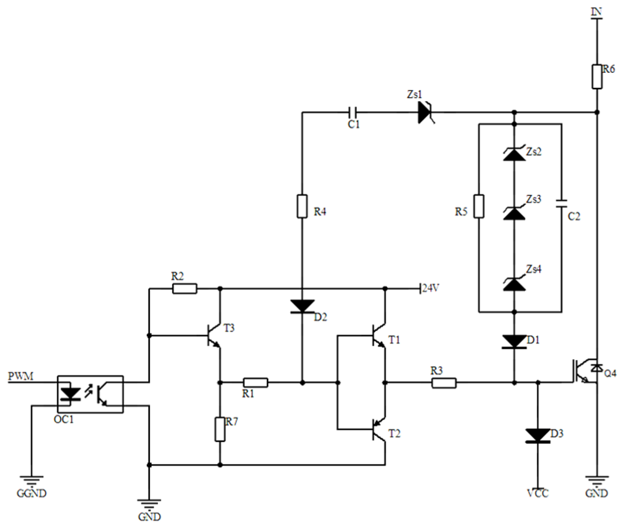
3. Overvoltage Suppression Circuit Combining an Active Clamp and Dynamic Feedback
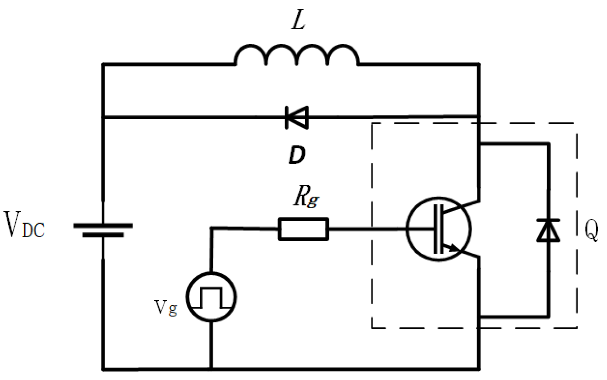
3.1. Circuit Design

As an improvement on the traditional overvoltage suppression circuit of an active clamp, the design idea of the overvoltage suppression circuit in this paper is as follows: (1) The overvoltage suppression circuit is composed of two independent parts: an active clamp and dynamic voltage feedback; (2) a capacitor is used to feedback the dynamic voltage rise rate; (3) the active clamp circuit is improved and the overvoltage feedback loop is increased; (4) a voltage source V C C is added to the IGBT gate to prevent the gate voltage from being too high due to feedback, and the gate voltage is clamped.
In summary, the designed active clamp and dynamic voltage feedback combined with the overvoltage suppression schematic diagram are shown in Figure 3. This figure includes an overvoltage suppression circuit and IGBT gate drive circuit. The overvoltage suppression circuit consists of the following parts: dynamic voltage rise rate feedback circuit composed of transient suppression diode Z s 1 and capacitor C 1 , and improved active clamping circuit composed of transient suppression diodes Z s 2 , Z s 3 , Z s 4 , capacitor C 2 and resistor R 5 ; IGBT grid drive circuit: a push-pull circuit composed of T 1 and T 2 triodes serves as the drive power amplifier of the grid, R 1 and R 3 are current limiting protection resistors, and OC1 is optocoupler for photoelectric isolation protection. In addition, D 1 and D 2 are universal diodes to prevent the IGBT gate signal from being shunted to the overvoltage suppression circuit.

3.2. Turn Off Voltage Spike Suppression Process

Before the IGBT is turned off, the whole circuit is in the on state, and the collector potential of the IGBT (Q4) is 0. Because of the action of the transient suppression diode, the active clamp and the dynamic voltage feedback circuit do not work. Figure 2 shows that at time t 0 , the IGBT control signal is inverted, and the circuit operation process is as follows: The switching waveform does not change from t 0 to t 1 , and the overvoltage suppression circuit stops working. The voltage and current of the IGBT at this stage meet the following requirements:
I T ( t ) = i L
V c e ( t ) = V o n
where V o n is the on-voltage drop of the IGBT in stage I.
From time t 1 , V c e starts to rise, and when V c e rises to the breakdown voltage U Z S 4 of the transient suppression diode Z s 4 , which is lower than the breakdown voltage of Z s 2 , Z s 3 and Z s 4 , Z s 4 is broken down, and capacitor C 2 begins to charge. Since C 2 is parallel to the Miller capacitance and much larger than the Miller capacitance, the Miller capacitance can be ignored, and the voltage rise speed of V c e can be slowed down. The voltage rise speed of V c e at this time can be expressed as follows:
d V c e d t = I g C 2
When V c e rises to the breakdown voltage U Z S 1 of Z s 1 , C 1 starts to charge. The current i C 1 flowing through C 1 can be expressed as follows:
i C 1 = C 1 d U c e d t
I C 1 passes through resistor R 4 . Because of the presence of the diode, i C 1 is fed back to the gate push–pull circuit composed of T 1 and T 2 to increase its current driving ability, reduce the falling rate of the gate voltage, and compensate for the delay of the entire active gate-driving circuit. At time t 3 , I T starts to drop. The voltage drop rate of the gate at this time directly reflects the change rate of I T , and the function of i C 1 is equivalent to increasing the value of I T , reducing the discharge speed of the gate, lessening the change rate of I T , and reducing the voltage spike; at the same time, since V c e exceeds the clamping voltage set by Z s 2 , Z s 3 and Z s 4 at time t 3 , the voltage spike appears, the transient suppression diodes Z s 2 , Z s 3 and Z s 4 of the active clamping circuit are simultaneously broken down, and the active clamping circuit starts to work. The voltage spike is absorbed by the active clamping circuit and fed back to the IGBT gate, thereby raising the gate voltage, stopping V c e from rising, and finally falling and stabilizing near the DC bus voltage of the circuit until the entire off process is completed.
From the characteristic curve of the IGBT observed during the whole turning-off process of the IGBT, the main function of the dynamic voltage feedback circuit is to prolong the voltage rise time of V c e . The main function of the active clamp circuit is to quickly react and compensate the IGBT gate after V c e reaches the voltage peak to pull down V c e , avoid an excessive voltage peak and protect the circuit.

4. Parameter Influence of the Dynamic Voltage Feedback Circuit

The influence of the parameters of the dynamic voltage feedback circuit on the turn-off characteristics of the IGBT at each stage during the turn-off process is shown in Table 1. Among them, Δ U c e is the difference between the off-voltage peak and the DC bus voltage, and R g is the off-resistance.

4.1. C 1 Impact Mechanism Analysis

As seen from Table 1, C 1 , R 4 and U Z S 1 have the most important influence on the performance of the dynamic voltage feedback circuit. To deeply study the influence of C 1 , R 4 and U Z S 1 on the dynamic voltage feedback circuit, we provide a basis for the parameter selection of the dynamic voltage feedback circuit, analyze the role of the dynamic voltage feedback circuit in each stage of the IGBT turn-off process, and list the corresponding expressions.
Table 1 shows that in stage III, C 1 , R 4 and U Z S 1 influence the turn-off voltage rise rate. When the IGBT is turned off in stage III, its collector–emitter voltage can be expressed as follows:
V c e ( t ) = V g e ( t ) + V g c ( t )
Since V c e continues to rise at this time, its value is related to V g e and V g c , and the values of V g e and V g c in stage III can be based on the following formulas:
V g c ( t ) = V m V c e o n + 1 C g c t 1 t i g c ( t ) V g e ( t ) = V L I g ( t ) R g
In Formula (8), V m is the Miller voltage, and V c e o n is the turn-on voltage of the IGBT. Since both voltages are fixed values, which are determined by the IGBT manufacturing process, the Miller capacitance C g c becomes an important factor at this time. After the dynamic voltage feedback circuit is added, after entering stage III, the transient suppression diode Z s 1 is reversely broken down, and capacitor C 1 begins to charge. At this time, the dynamic feedback circuit is turned on, and C 1 is equivalent to being connected in parallel with both ends of C g c . The value is much larger than C g c , raising the Miller capacitance value of the IGBT and thereby reducing V g c . Since the dynamic voltage feedback circuit feeds back the gate current of the IGBT as i C 1 , I g (t) = i C 1 + i g increases accordingly, V g e decreases, and finally V c e decreases, suppressing the voltage spike.
When setting the value of capacitor C 1 constant, the current discharged through C 1 can be obtained from Formula (6), which acts on the push–pull circuit of the control pole, according to the output characteristic curve of the triode. When the triode works in the amplification area, the base current of the triode increases, the emitter current also increases, and finally, the IGBT gate current increases. According to Formula (8), V g e decreases, which reduces V c e . From the changes in V g c (t) and V g e (t) in Formula (8), it can be concluded that when R 4 and U Z S 1 remain unchanged and C 1 increases, the values of V g e and V g c will decrease, resulting in a decrease in V c e . The simulation platform shown in Figure 3 is built in SABER, and the simulation diagrams in Figure 4 and 5 represent the V g e and V c e turn-off waveforms corresponding to different C 1 values, respectively. The change in C 1 has a substantial impact on the turn-off voltage spike. Figure 4 shows that the larger the value of C 1 is, the lower the rising rate of V c e , which reduces the voltage spike; Figure 5 shows that the larger the value of C 1 is, the smaller the drop rate of V g e will be. Additionally, the later the active clamp circuit will be triggered to work, the longer the time for raising the gate voltage at time t 3 will be, and at the same time, the smaller the gate voltage will be.
Set R 4 and U Z S 1 unchanged, change the value of C 1 , and then conduct multiple groups of simulations to obtain the curve of voltage spike V c e ( m a x ) changing with C 1 as shown in Figure 6. It can be seen that when C 1 < 400 pF, the change of C1 has a significant impact on V c e ( m a x ) ; when C 1 > 400 pF, it has little effect on V c e ( m a x ) . This shows that the suppression circuit can reduce the voltage spike, but can not completely eliminate the turn off voltage spike.

4.2. R 4 Impact Mechanism Analysis

R 4 mainly affects the charging and discharging time of the capacitor and the feedback current in the dynamic voltage feedback circuit, wherein the charging and discharging expression of the capacitor is as follows:
τ = R C U C C = U × [ 1 e ( t / τ ) ] U C D = U 0 × e ( t / τ )
where τ is the charge time constant, U is the power supply voltage, U 0 is the voltage on the capacitor before discharge, U C C is the charge voltage value at time t on capacitor C 1 , and U C D is the discharge voltage value of the capacitor.
The discharge current can be expressed as as follows:
I = U C D / R
According to Formulas (9) and (10), R 4 affects the off-voltage spike. Changing the size of R 4 will affect the discharge voltage value of capacitor C 1 at any time and change the size of the feedback current, thus causing the rise rate of V g e to change and affecting the voltage spike of V c e . Figure 7 and Figure 8 show the simulation waveform images of V c e and V g e , respectively, when the size of R 4 is changed under the condition of constant C 1 and U Z S 1 .
The also figure shows that with an increase in the value of R 4 , the rising rate of V c e will be larger, resulting in a larger voltage spike of V c e , which will trigger the active clamp circuit earlier, and at the same time, the falling rate of V g e will also be larger, resulting in V g e at time t 3 , a larger voltage boost appears to suppress the voltage spike.
Change the size of R 4 for many times, keep C 1 and U Z S 1 unchanged, and get the curve of V c e ( m a x ) changing with R 4 as shown in Figure 9. It can be seen that R 4 has the same effect on V c e ( m a x ) as C 1 , but the change rate of V c e ( m a x ) is small.

4.3. U Z S 1 Impact Mechanism Analysis

Setting the values of C 1 and R 4 as constant, the effects of different values of U Z S 1 on V c e and V g e are shown in Figure 10 and Figure 11. Through multiple groups of simulations, the curve of V c e ( m a x ) versus U Z S 1 in Figure 12 can be obtained.The effect of U Z S 1 on V c e is small. The figure shows that the smaller U Z S 1 is, the longer the duration of stage III, resulting in longer off-time, resulting in additional losses that do not affect the value of V c e . At this time, the turn-off loss of the IGBT can be expressed as follows:
E o f f = t 0 t 3 u c e ( t ) · i c ( t ) d t
Assuming that the rise of IGBT collector voltage in this process is linear, Equation (11) can be expressed as follows:
E o f f = i c · ( t 3 t 0 ) · ( u c e ( t 3 ) u c e ( t 0 ) ) 2
T 3 and t 0 are the time points when the IGBT starts to turn on and completely turns off, respectively. Where u c e (t) is the voltage of each time period when the IGBT is turned off and i c (t) is the current of each time period when the IGBT is turned off. Since u c e (t) and i c (t) are related to d U c e /dt, the additional loss caused by the IGBT increases with the decrease in d U c e /dt of the IGBT.

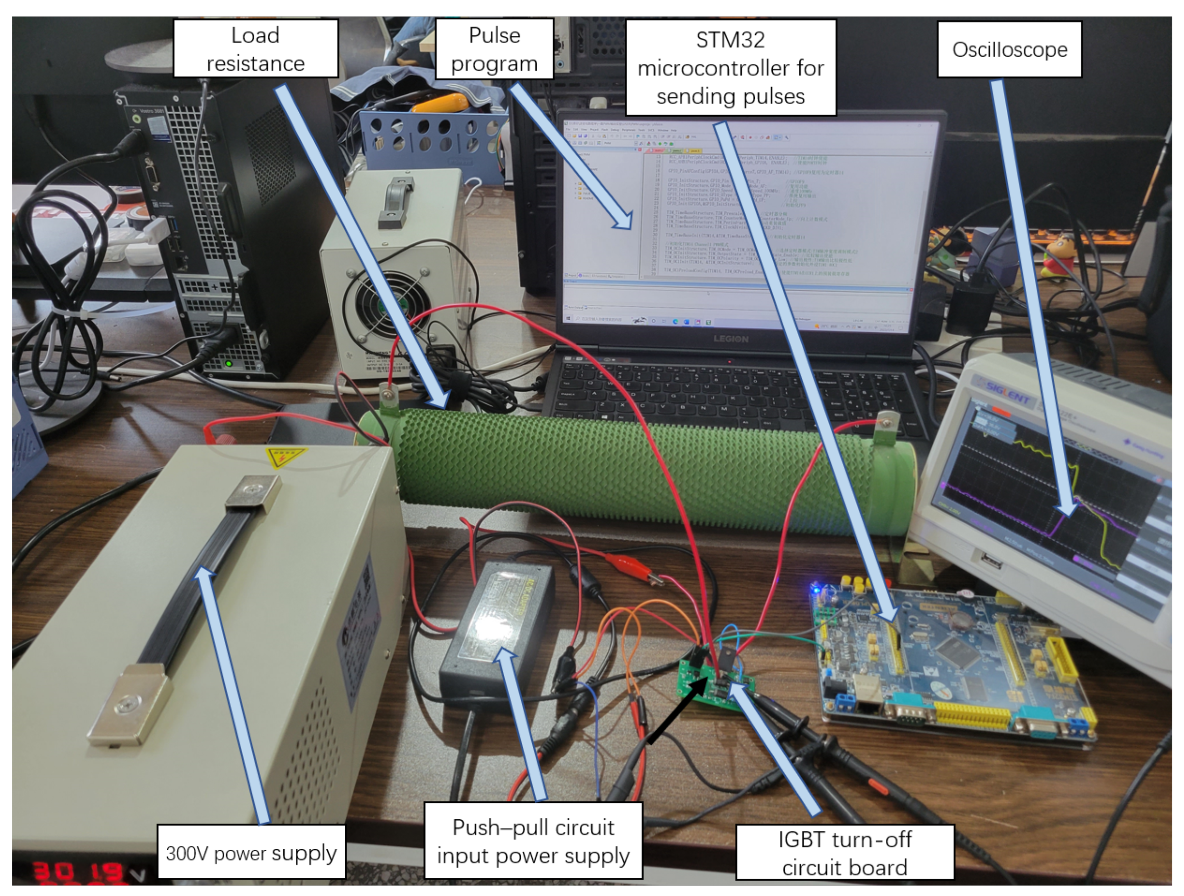
5. Experimental Analysis

To test the influence of the parameters of the dynamic voltage feedback circuit on the voltage spike and gate voltage during the turn-off transient of the IGBT, the experimental platform shown in Figure 13 was built according to Figure 3 for the experiment, and the IGBT model GF10NC60KD was selected for test comparison and analysis. Its rated voltage is 600 V, collector current i c = 20 A ( T j = 25 °C), saturation voltage drop V C E ( s a t ) = 2.2 V, threshold voltage V G ( t h ) = 4.5 6.5 V, gate drive voltage V G E = ±20 V. The input signal of the push–pull circuit selects 24V DC power supply. IGBT test input DC bus voltage V d = 300 V, and selects 300 V DC power supply with power of 1500 W as its input.

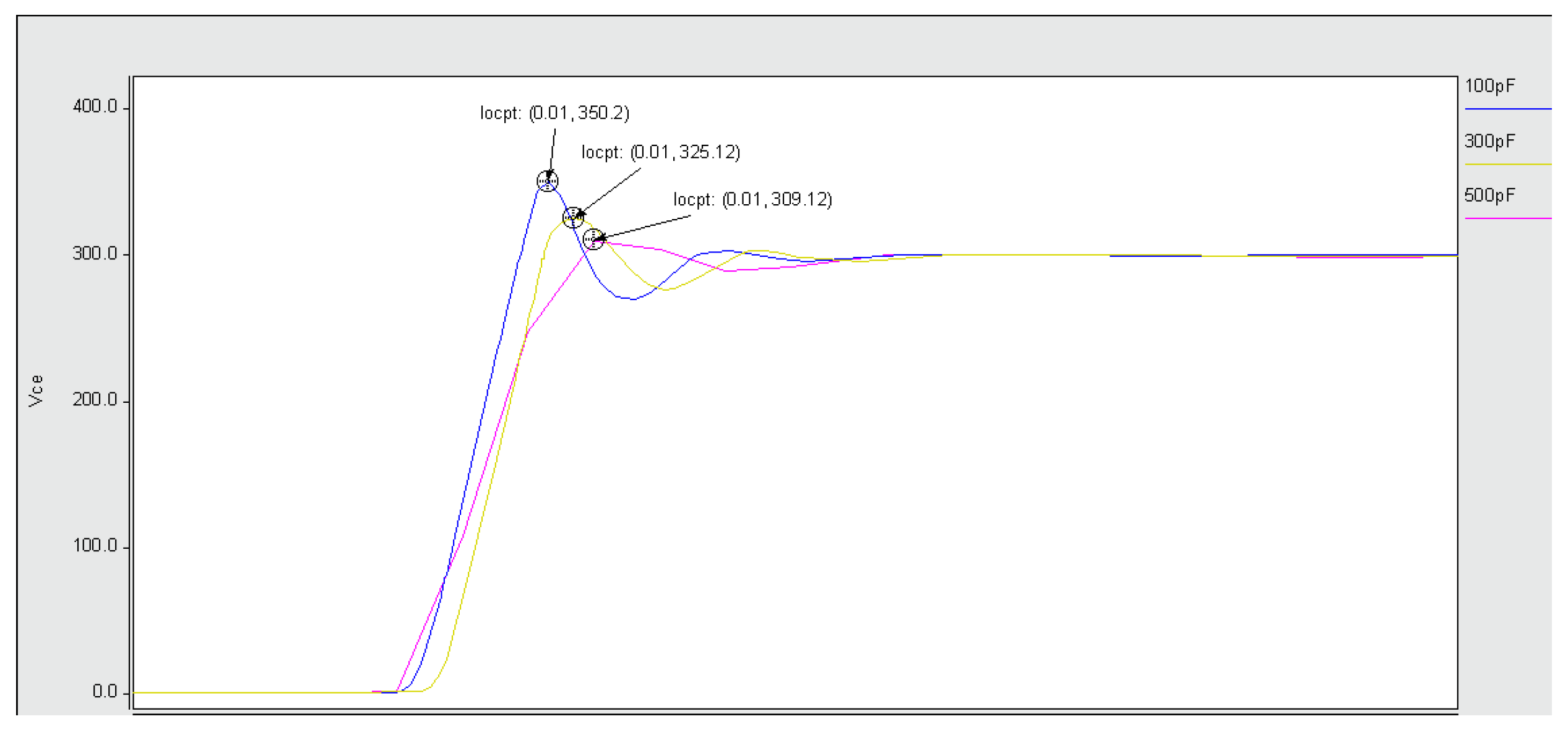
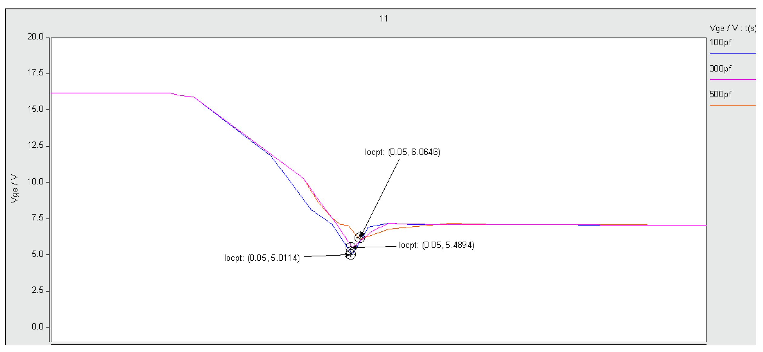
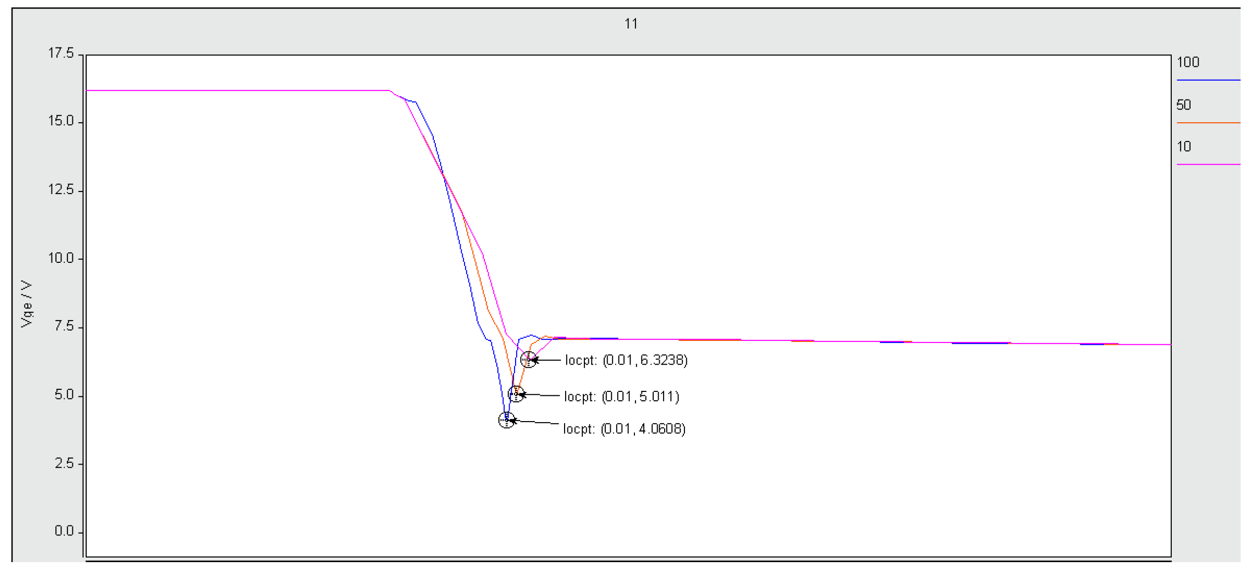
5.1. Influence of Capacitance on the Performance of a Dynamic Voltage Feedback Circuit

To analyze the suppression effect of capacitance on the IGBT voltage spike and the influence of the gate signal in the dynamic voltage feedback circuit, set U Z S 1 = 100 V, R 4 = 100 Ω , U Z S 2 = 300 V, where U Z S 2 is the clamping voltage set by Z S 2 , Z S 3 and Z S 4 in the circuit. We obtain the waveform images of V c e and V g e in Figure 14 when C 1 = 100 pF, and key parameters of IGBT shutdown in Table 2, where V c e is measured with the × 10 probe of the oscilloscope. Figure 15 is a waveform image when only C 1 = 500 pf is changed. A comparison shows that the change in C 1 has a significant impact on the voltage spike of V c e . When C 1 = 100 pF, the maximum value of V c e is 382 V, and when C 1 = 500 pF, the maximum value of V c e is 346 V. First, the larger the value of C 1 is, the longer the time from t 0 to t 3 will be, which will lead to a decrease in d i c /dt, and in turn reduces the voltage spike of V c e , which has a better suppression effect. At this time, the dynamic voltage feedback circuit behaves as a pair of d i c /dt suppression effects of the IGBT.
The main function of the feedback signal of the dynamic voltage feedback circuit is to increase the gate signal, which is manifested as the influence of increasing the slope of d V g e /dt, while the active clamp circuit manifests as a direct lift effect on the gate signal. When the IGBT turn-off voltage exceeds the U Z S 2 set by the active clamp circuit, the gate signal will have a substantial rise. The experimental waveforms with C 1 of 100 pF (Figure 14) and 500 pF (Figure 15) show that the larger the value of C 1 is, the smaller the d V g e /dt, the longer the time for V c e to reach the voltage peak, and the later the time to trigger turning on the active clamp circuit.

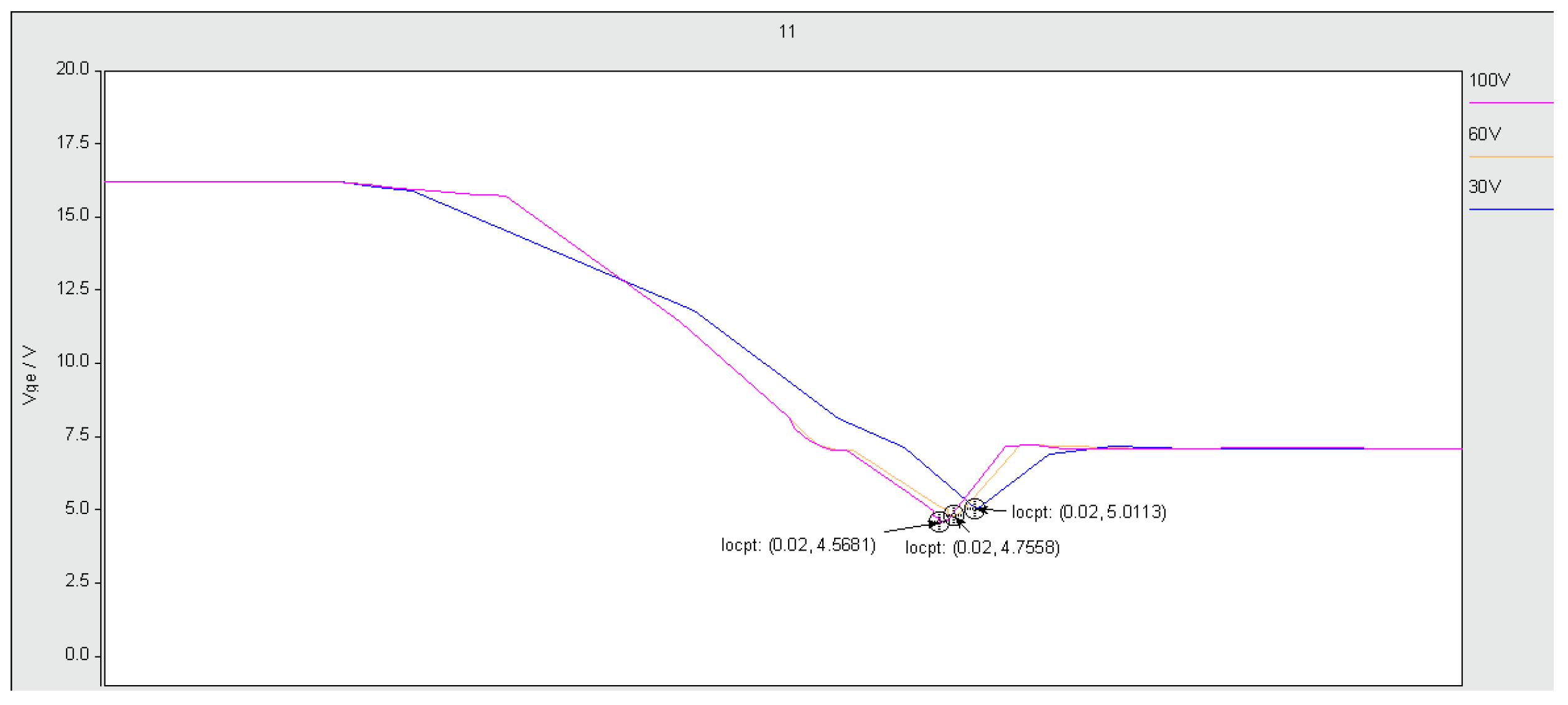
5.2. Effect of Resistors on the Performance of Dynamic Voltage Feedback Circuits

We set U Z S 1 = 100 V, U Z S 2 = 300 V, C 1 = 100 pF, change the value of R 4 , and obtain the IGBT turn-off waveform when R 4 = 10 Ω , as shown in Figure 16, and key parameters in Table 3 are obtained. Compared with the turning-off waveform of the IGBT when the resistance R 4 = 100 Ω in Table 2, it was found that as the resistance R 4 decreases from 100 Ω to 10 Ω , the turning-off voltage peak of the IGBT decreases from 382 V to 368 V, and the rising slope of the IGBT V c e decreases during the turning-off process. According to the analysis in Chapter 3, this decrease occurs because increasing the resistance prolongs the charge and discharge time of the capacitor and reduces the current fed back to the gate.
The influence of resistance on the gate signal in the dynamic voltage feedback circuit is analyzed. Compared with R 4 = 100 Ω (Figure 14) and R 4 = 10 Ω (Figure 16), the change in R 4 affects the change in V g e . The smaller the R 4 value is, the slower the decline rate of V g e . In Figure 11, t 3 - t 0 = 550 ns; in Figure 13, t 3 - t 0 = 2.2 µs. During the IGBT off process, with the decrease in R 4 , the feedback signal of the gate increases, which decreases d V g e /dt, and finally extends the time beyond the DC bus voltage V d to reduce the voltage spike. The gate needs to feed back a small voltage signal through the active clamp circuit to suppress the voltage spike.

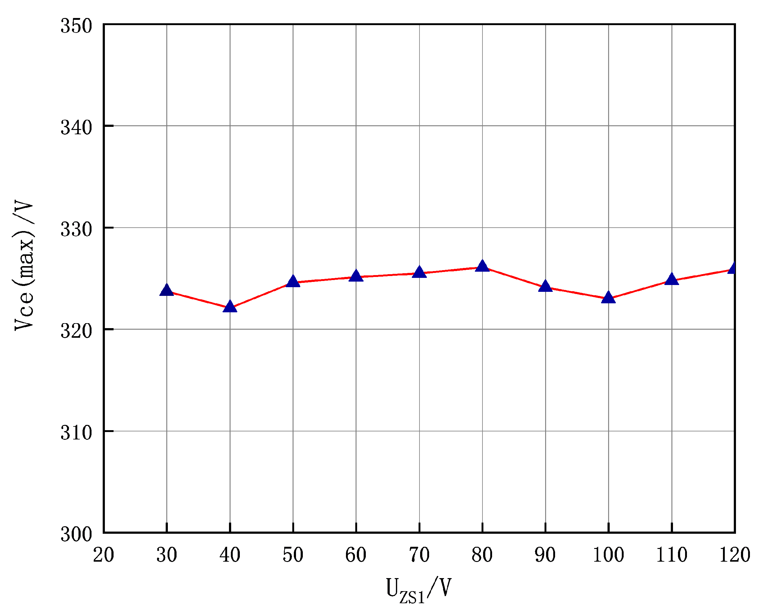
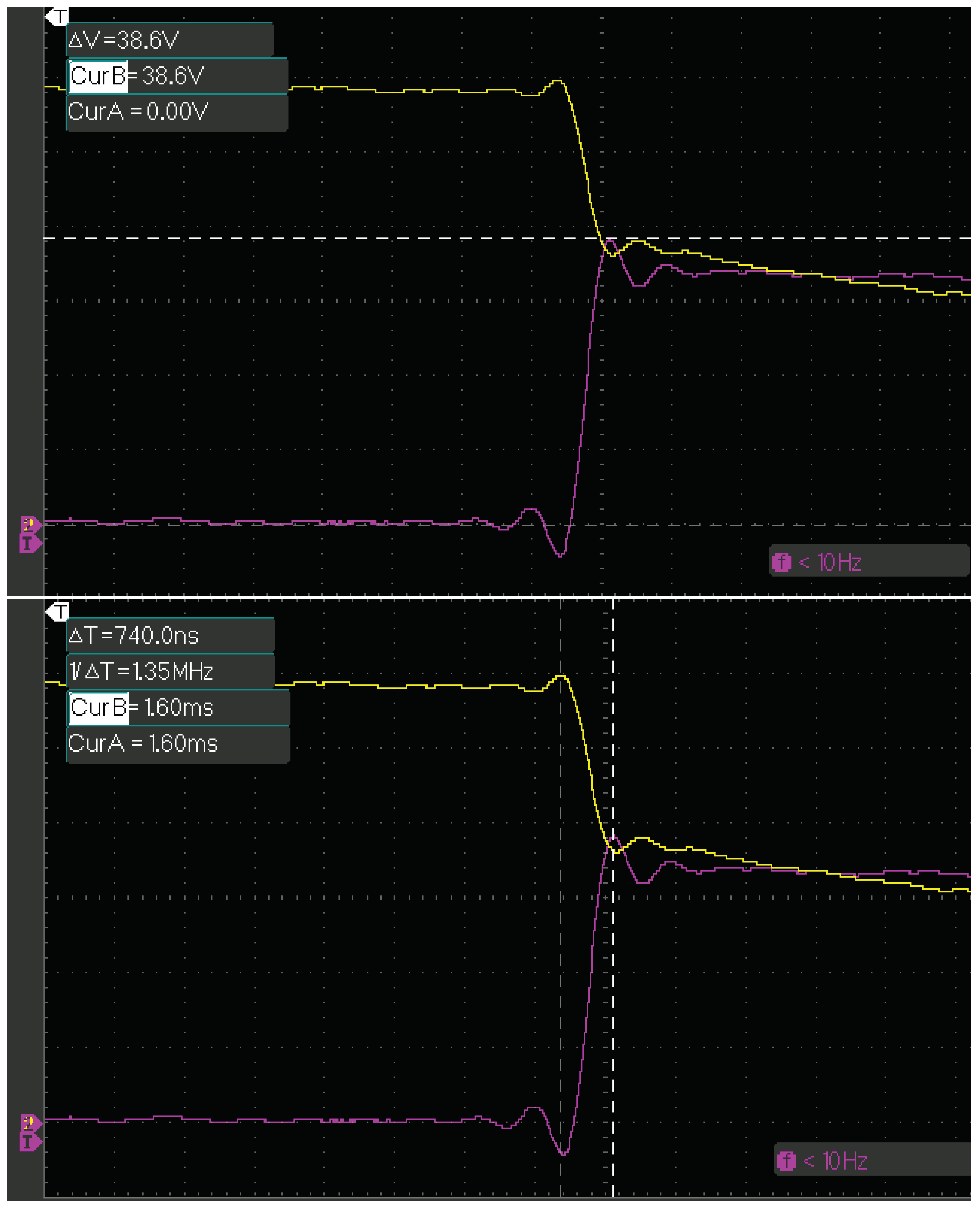
5.3. Effect of UZS1 on the Performance of the Dynamic Voltage Feedback Circuit

Figure 17 shows the waveform images of V c e and V g e of the IGBT in the off process when U Z S 1 = 100 V, R 4 = 100 Ω, U Z S 2 = 300 V, C 1 = 100 pF and U Z S 1 = 60 V are changed. From the key parameters in Table 4, it can be seen that U Z S 1 has little effect on the voltage spike of V c e . After the value of U Z S 1 is increased from 30 V to 60 V, the voltage spike of V c e is 386 V, which is almost unchanged. In addition, the smaller U Z S 1 is, the longer the time from time t 0 to time t 3 . In Figure 14, t 3 - t 0 = 550 ns, while in Figure 17, t 3 - t 0 = 740 ns, which leads to an extension of the off time of the IGBT and further generates additional losses.

6. Conclusions

(1)
Aiming at the problem of off-voltage spikes in IGBT applications, a voltage spike suppression circuit combining dynamic voltage feedback and an active clamp is proposed. The voltage rise rate of the IGBT is fed back by the capacitor to solve the problem of feedback signal delay in the circuit. Combined with the active clamp circuit, the voltage spike is suppressed to ensure safe and reliable operation of the IGBT.
(2)
Research and analysis show that adjusting C 1 and R 4 in the dynamic voltage feedback circuit can clearly suppress the off-voltage spike.
(3)
The experimental results show that by increasing the value of C 1 and decreasing the value of R 4 , the signal fed back to the IGBT gate by the dynamic voltage feedback circuit is increased to reduce the voltage rise rate and the turn-off voltage peak of the IGBT during the turn-off process. Changing U Z S 1 cannot reduce the off-voltage spike of the IGBT.

Author Contributions

This paper has six authors and their names and contributions to the paper are: M.C. (writing, and preparation of original draft), Z.X. (writing, reviewing, and editing the whole paper), Y.Z. (Yongxia Zhang) (editing and helping with the revisions), E.Z., Y.Z. (Yuying Zhao) and Z.M. (editing and helping with the revisions). All authors have read and agreed to the published version of the manuscript.

Funding

This work was supported in part by the National Natural Science Foundation of China, under Grants 51965029.

Institutional Review Board Statement

Not applicable.

Informed Consent Statement

Not applicable.

Data Availability Statement

Not applicable.

Conflicts of Interest

The authors declare no conflict of interest.

References

  1. Singh, M.D. Power Electronics; Tata McGraw-Hill Education: New York, NY, USA, 2008. [Google Scholar]
  2. Engelmann, G.; Lüdecke, C.; Bündgen, D.; De Doncker, R.W.; Lu, X.; Xu, Z.; Zou, K. Experimental analysis of the switching behavior of an IGBT using a three-stage gate driver. In Proceedings of the IEEE 8th International Symposium on Power Electronics for Distributed Generation Systems, Florianopolis, Brazil, 17–20 April 2017; pp. 1–8. [Google Scholar]
  3. Zhou, Y.; Chen, L.; Yang, S.; Xu, F.; Khorshed, A. A low cost gate driver with dynamic turn-off transient control for HEV/EV traction inverter application. In Proceedings of the IEEE Applied Power Electronics Conference and Exposition, Tampa, FL, USA, 26–30 March 2017; pp. 3200–3204. [Google Scholar]
  4. Alam, M.; Kumar, K.; Dutta, V.J. Comparative efficiency analysis for silicon, silicon carbide MOSFETs and IGBT device for DC–DC boost converter. SN Appl. Sci. 2019, 1, 1700. [Google Scholar] [CrossRef] [Green Version]
  5. Yang, X.; Lei, L. Mechanism analysis of IGBT turn-on process. J. Phys. Conf. Ser. 2019, 1237, 032074. [Google Scholar] [CrossRef]
  6. Tiwari, A.; Antoniou, M.; Trajkovic, T.; Dai, T.; Gammon, P.M.; Udrea, F. Transient Performance of >10 kV SiC IGBT with an Optimized Retrograde p-Well. In Unspecified; Materials Science Forum; Trans Tech Publications Ltd.: Bäch, Switzerland, 2020; Volume 1004, pp. 917–922. [Google Scholar]
  7. Yang, X.; Yuan, Y.; Long, Z.; Goncalves, J.; Palmer, P.R. Robust stability analysis of active voltage control for high-power IGBT switching by Kharitonov’s theorem. IEEE Trans. Power Electron. 2015, 31, 2584–2595. [Google Scholar] [CrossRef]
  8. Ning, P.; Yuan, T.; Kang, Y.; Han, C.; Li, L. Review of Si IGBT and SiC MOSFET based on hybrid switch. Chin. J. Electr. Eng. 2019, 5, 20–29. [Google Scholar] [CrossRef]
  9. Erickson, R.W.; Maksimovic, D. Fundamentals of Power Electronics; Springer Science & Business Media: Berlin/Heidelberg, Germany, 2007. [Google Scholar]
  10. Kasiran, A.N.; Ponniran, A.; Bakar, A.A.; Yatim, M.H.; Noor, M.K.R.; Jumadril, J.N. Implementation of Resonant and Passive Lossless Snubber Circuits for DC-DC Boost Converter. Int. J. Eng. Technol. 2018, 7, 246–252. [Google Scholar] [CrossRef]
  11. Abdalgader, I.A.S.; Kivrak, S.; Özer, T. Power Performance Comparison of SiC-IGBT and Si-IGBT Switches in a Three-Phase Inverter for Aircraft Applications. Micromachines 2022, 13, 313. [Google Scholar] [CrossRef] [PubMed]
  12. Zhu, Y.; Xiao, M.; Su, X.; Yang, G.; Lu, K.; Wu, Z. Modeling of conduction and switching losses for IGBT and FWD based on SVPWM in automobile electric drives. Appl. Sci. 2020, 10, 4539. [Google Scholar] [CrossRef]
  13. Jin, R.; Cui, L.; Gong, C.; Wu, Y. Simulation Study on High-Voltage IGBT Turn-Off with Polysilicon Distributed Gate Resistance Effect; Atlantis Press: Amsterdam, The Netherlands, 2019; pp. 82–85. [Google Scholar]
  14. Panneerselvam, S.; Srinivasan, B. Switching loss analysis of IGBT and MOSFET in single phase PWM inverter fed from photovoltaic energy sources for smart cities. Int. J. Syst. Assur. Eng. Manag. 2022, 13, 718–726. [Google Scholar] [CrossRef]
  15. Vijayalakshmi, A. Improved Trans-Z-source inverter based dynamic voltage restorer. Aust. J. Electr. Electron. Eng. 2022, 19, 22–30. [Google Scholar] [CrossRef]
  16. Shu, L.; Zhang, J.; Peng, F.; Chen, Z. Active current source IGBT gate drive with closed-loop di/dt and dv/dt control. IEEE Trans. Power Electron. 2016, 32, 3787–3796. [Google Scholar] [CrossRef]
  17. He, Y.; Luo, H.; Qin, R.; Luo, X.; Yao, Y.; Wen, G.; Xiao, Q.; Tan, C. A split-gate trench IGBT with low Miller capacitance and dV/dt noise. J. Comput. Electron. 2021, 20, 568–574. [Google Scholar] [CrossRef]
  18. Ghorbani, H.; Sala, V.; Paredes Camacho, A.; Romeral Martinez, J.L. A Simple Closed-Loop Active Gate Voltage Driver for Controlling diC/dt and dvCE/dt in IGBTs. Electronics 2019, 8, 144. [Google Scholar] [CrossRef] [Green Version]
  19. Mannen, T.; Wada, K.; Obara, H.; Miyazaki, K.; Takamiya, M.; Sakurai, T. Active gate control for switching waveform shaping irrespective of the circuit stray inductance in a practical full-bridge IGBT inverter. In Proceedings of the IEEE Applied Power Electronics Conference and Exposition, San Antonio, TX, USA, 4–8 March 2018; pp. 3108–3113. [Google Scholar]
  20. Krishna, D.; Agarwal, V. Active gate control of series connected IGBTs using positive current feedback technique. IEEE Trans. Circuits Syst. II Express Briefs 2005, 52, 261–265. [Google Scholar] [CrossRef]
  21. Bortis, D.; Biela, J.; Kolar, J.W. Active gate control for current balancing of parallel-connected IGBT modules in solid-state modulators. IEEE Trans. Plasma Sci. 2008, 36, 2632–2637. [Google Scholar] [CrossRef]
  22. Zarghani, M.; Mohsenzade, S.; Kaboli, S. A series stacked IGBT switch based on a concentrated clamp mode snubber for pulsed power applications. IEEE Trans. Power Electron. 2019, 34, 9573–9584. [Google Scholar] [CrossRef]
  23. Deng, G.; Ma, Z.; Luo, X.; Xie, X.; Li, C.; Ng, W.T. A Novel IGBT With Voltage-Clamping for Turn-on Overshoot Suppression Under Hard-Switching. IEEE Trans. Electron Devices 2021, 68, 5326–5329. [Google Scholar] [CrossRef]
Figure 1. IGBT typical application circuit.
Applsci 13 00795 g001
Figure 2. IGBT turn-off process curve.
Applsci 13 00795 g002
Figure 3. Overvoltage suppression schematic.
Applsci 13 00795 g003
Figure 4. V c e comparison diagram under different C 1 values.
Applsci 13 00795 g004
Figure 5. V g e comparison diagram under different C 1 values.
Applsci 13 00795 g005
Figure 6. Curve of V c e ( m a x ) changing with C 1 .
Applsci 13 00795 g006
Figure 7. V c e comparison diagram under different R 4 values.
Applsci 13 00795 g007
Figure 8. V g e comparison diagram under different R 4 values.
Applsci 13 00795 g008
Figure 9. Curve of V c e ( m a x ) changing with R 4 .
Applsci 13 00795 g009
Figure 10. V c e comparison diagram under different U Z S 1 values.
Applsci 13 00795 g010
Figure 11. V g e comparison diagram under different U Z S 1 values.
Applsci 13 00795 g011
Figure 12. Curve of V c e ( m a x ) changing with U Z S 1 .
Applsci 13 00795 g012
Figure 13. IGBT turn-off experiment.
Applsci 13 00795 g013
Figure 14. C 1 = 100 pF turn-off waveform.
Applsci 13 00795 g014
Figure 15. C 1 = 500 pF turn-off waveform.
Applsci 13 00795 g015
Figure 16. R 4 = 10 Ω turn-off waveform.
Applsci 13 00795 g016
Figure 17. U Z S 1 = 60 V turn-off waveform.
Applsci 13 00795 g017
Table 1. Influence of parameters on turn-off characteristics at various stages.
TimeRegular ConstantDynamic Voltage Feedback ParametersResult
t 0 t 1 R g NoneTurn-off delay
t 1 t 2 R g Noned U c e /dt
t 2 t 3 R g d U c e /dt C 1 R 4 U Z S 1 d U c e /dt
t 3 t 4 R g d U c e /dt C 1 R 4 Δ U c e d I c /dt
Table 2. Influence of C 1 on the turn off characteristics.
C 1 R 4 U ZS 1 t 3 - t 0 V ce
100 pF100 Ω100 V550 ns382 V
500 pF100 Ω100 V1080 ns346 V
Table 3. Influence of R 4 on the turn off characteristics.
C 1 R 4 U ZS 1 t 3 - t 0 V ce
100 pF10 Ω100 V2200 ns368 V
Table 4. Influence of U Z S 1 on the turn off characteristics.
C 1 R 4 U ZS 1 t 3 - t 0 V ce
100 pF100 Ω60 V740 ns386 V
Disclaimer/Publisher’s Note: The statements, opinions and data contained in all publications are solely those of the individual author(s) and contributor(s) and not of MDPI and/or the editor(s). MDPI and/or the editor(s) disclaim responsibility for any injury to people or property resulting from any ideas, methods, instructions or products referred to in the content.

