1. Introduction
Parametric amplifiers (PAs) are known as ultimate low-noise amplifiers; however, such conventional cavity-based amplifiers are burdened with a gain-bandwidth trade-off. To overcome the drawback, traveling-wave parametric amplifiers (TWPAs) were suggested. TWPAs are based on using waveguide lines with nonlinear reactive parameters (of capacitive or inductive types) such as a kinetic inductance microwave line [
1] or artificial lines composed of lumped cells with nonlinear capacitors or inductances. As the superconducting kinetic inductance of Josephson junctions
) is strongly nonlinear (here,
,
, and
is the Josephson junction critical current and
is the Josephson junction phase), the artificial lines composed of superconducting cells containing Josephson junctions are generally used in the designs of Josephson traveling-wave parametric amplifiers (JTWPAs) [
2,
3,
4,
5,
6,
7,
8,
9,
10,
11,
12]. The amplifiers capable of working at low and very low temperatures can provide the extremely high sensitivity approaching the quantum limit level. Therefore, JTWPAs are currently considered as promising readout devices for use in the field of precision quantum measurements (including single-photon detectors), quantum communications and quantum computing (see [
13,
14] and review [
15]).
However, when the pump and signal waves propagate in the common artificial Josephson line of JTWPAs, the attainable gain is limited by depletion of the pump wave [
8,
9,
15] because the initial amplitude of the pump wave is restricted by critical current values of the used Josephson junctions. To overcome this problem, a two-line JTWPA design with a magnetic flux drive was suggested [
16]. In the design, a separate non-Josephson (linear) transmission line is used for the pump wave propagation. This line is inductively coupled with SQUID-like cells of the signal artificial line and, therefore, the pump wave produces a traveling wave of magnetic flux applied to the signal line cells. This magnetic flux wave provides modulation of the cell inductances in the traveling-wave fashion.
In this paper, we discuss the characteristics of the artificial waveguide lines composed of lumped element cells in connection with designing the Josephson traveling wave parametric amplifiers and consider the increase in dynamic range of the two-line flux-driven amplifier by substitution of dc SQUID cells for bi-SQUID cells.
2. Effect of Finite Size of Artificial Cells
Usually, the JTWPA designs are based on implementation of the artificial right-handed lines containing Josephson junctions, although the left-handed artificial lines can also be used as recently reported in [
17]. The right-handed artificial lines correspond to the existing natural distributed waveguide lines. Therefore, the natural distributed lines are often modeled by the right-handed artificial LC lines under the stipulation that the length of the distributed line pieces described by the lumped LC cells goes to zero. The limit processing (when
) leads to telegrapher’s equations and hence to the differential wave equation [
18].
However, when the lumped cells of the implemented artificial lines model the continuous line pieces of finite length, one should describe the discrete system using discrete-valued equations as it is realized in [
19] (versus continuum approximation in [
12]) and partly in [
16]. Nevertheless, to simplify analysis of the artificial network, many authors consider the structure as a really distributed continuous waveguide line to describe propagation of the pumping, signal and idler waves in the artificial structure using a wave-type equation for a continuous medium. In the approach, wave impedance of the artificial line is considered as a real-value impedance
Z0 of the corresponding really distributed waveguide line. However, this is generally incorrect.
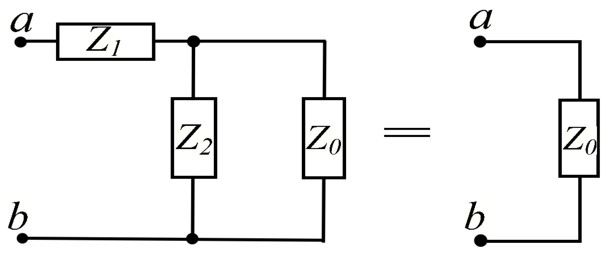
Figure 1 illustrates simple reasoning which can be used to calculate wave impedance of the long artificial line, consisting of
Z1,
Z2 -cells. If
Z0 is the wave impedance, then it does not change with connection of the same additional cell. This requirement yields in the following equation:
In case of a conventional dissipativeless cell line with the cell element impedances
and
, the wave impedance of the artificial line is complex:
where the angle
changes from
at
to
at cutoff frequency
Thus, the wave impedance changes from the real value
at a low frequency to the imaginary value
i at
. This fact means that the artificial cell line cannot be matched with any constant real-valued impedance over the total frequency band up to the cutoff frequency. For example, when the cell line is connected to the real-valued impedance
, the reflection factor is imaginary and frequency-dependent:
The absolute magnitude of the factor changes from at to at . Of course, the problem vanishes with decreasing the cells’ size (at and ), i.e., with limit processing of the distributed waveguide line when .
To mitigate the reflection problem, one could increase the cutoff frequency of the artificial line as compared with frequencies of the pumping, signal and idler signals; however, it additionally leads to the intense depletion of the pump wave due to the unwanted leak of the pump power to the higher harmonics and intermodulation components occurring in the frequency band ranging up to the cutoff frequency. Moreover, the described dependence of the wave impedance on frequency automatically leads to the frequency-dependent phase velocity decreasing with frequency.
2.1. One-Line Amplifier Design
In the three-wave operation mode when , finding the reasonable trade-off seems very problematic because both the wave reflection and the phase mismatch of the pumping, signal and idler waves enforce setting the cutoff frequency much higher than the wave frequencies, but it does not allow for keeping the higher harmonics and the intermodulation components out of the frequency band. The restrictions can be mitigated by using the four-wave operation mode when . In this case, all three frequencies can be located nearer to each other in the vicinity of so that both the harmonics and the intermodulation components produced by the Kerr nonlinearity are above the cutoff frequency, and the reflection factor (at ) is quite moderate: . At the same time, the frequency closeness makes the efficient filtering out of the pump frequency from the amplified signal more difficult.
2.2. Two-Line Amplifier Design
The flux-driven JTWPA with two-line amplifier design suggested in [
16] consists of two coupled separate artificial waveguide lines. The first artificial LC line, where both the signal and idler waves propagate, is based on using a serial array of dc SQUIDs coupled inductively to the second superconducting LC transmission line carrying the pumping wave. The latter is linear (non-Josephson) and therefore is free from any limitation on the pump wave amplitude and from energy leakage to higher harmonics as well. The pump signal applies rf magnetic flux
to the SQUID cells and, due to the cells’ nonlinear properties, provides modulation of the dipole cell inductances
(with a depth
m) in the wave manner through influence of the maximum superconducting current
of the dc SQUID cell. The inductance modulation can be provided either on the pump frequency when a dc flux bias
is additionally applied:
or on the double frequency when no dc flux is applied (
):
However, in the latter case, the modulation depth
is considerably less than
due to the approximately
-like dependence [
20] of the maximum superconducting current
of dc SQUID on the applied magnetic flux
. At a low loop inductance (as assumed in [
16]),
, where
, and hence at
where
and
are the normalized values of the applied dc and rf magnetic fluxes. This expression shows that dc flux changes the maximum superconducting current (from
to
) and hence the dipole inductance of dc SQUID and modulation of the inductance from (7) to (6) with a modulation depth about four times higher.
The inductance modulation waves (6) and (7) yield in the signal frequency mixing either to
or to
corresponding to the three-wave and four-wave operation modes, when
is the signal frequency and the idler frequency is
or
, respectively. In both cases, the signal and idler wave frequencies can be optimally located in the vicinity of
, where the reflection factor is moderate,
, and the phase velocities of the waves are quite close to each other:
(with using dimensionless coordinate
x normalized on the cell length “
a”), and therefore they can be tuned closely to the phase velocity of the pump wave propagating in the second line. For example, when one sets the pump frequency as
in three-wave mode or
in four-wave mode, the signal and idler frequency band can range from
to
, that enables eliminating wave components at frequencies
and
, respectively, and the reflection factor at signal frequency
and idler frequency
decreases to
.
Figure 2 shows the reflection factor
for the artificial waveguide line of lumped L and C elements which is connected to resistor
, as well as optimal values of both the pump wave frequency
in the three-wave mode (or double frequency
in the four-wave mode) and the frequency range for signal and idler waves.
3. Increase in Dynamic Range Using bi-SQUID Cells
The dynamic range (DR) of an amplifier can be defined as the maximum-to-minimum ratio of the output signal power within the range of the linear relation between the output signal and input signal, starting from the minimum value of the output signal amplitude restricted by the root-mean-square (rms) value of the output noise.
Although the gain of the flux-driven JTWPA is not restricted by the pump wave depletion, the output signal power is inevitably limited by nonlinear distortions as the
rf current amplitude increases and nears the maximum superconducting current of the cells (as inductances) in use, namely dc SQUIDs suggested in [
16]. In fact, a linear wave-type equation with a periodically modulated reactive parameter, which was derived in [
16] for the magnetic flux
in the frame of distributed line approximation (using dimensionless coordinate
x normalized on the cell spacing “
a”), gives an exponential increase in amplitudes with
x of both the signal and idle traveling flux waves
and
. However, to obtain an output power, one needs to know the amplitude of the current traveling waves
and
. The relation between the flux and current amplitudes,
and
, is linear at low values:
, where
k is the wave number (reduced to the reciprocal of the cell spacing),
is the running inductance (dipole inductance of SQUID-cell) and
is amplitude of the flux per unit length. But this ratio becomes nonlinear with an increase in the wave amplitudes and then the current wave amplitude can be written as
. This leads to the power gain reduction by factor
rising the current amplitude nearing the maximum superconducting current value of the SQUID cells in use. The linear domain limit determines the dynamic range of the amplifier. The end point of the linear range can be characterized by the signal amplitude corresponding to the power gain reduction by 1 dB; this is called the 1 dB compression point.
Increasing the critical current
of the used Josephson junctions to increase the maximum superconducting current of the SQUID cells cannot be an acceptable solution for extending the linear domain, because the critical current magnitude determines some other normalized parameters answering for the amplifier’s performance. For example, one has to increase geometric loop inductance in order to increase the flux applied by the pumping wave, but one has to decrease the normalized value of the loop inductance
by decreasing the junction critical current to increase both the modulation depth of the maximum superconducting current of the cell and the characteristic Josephson junction inductance
and hence the modulation depth of the dipole cell inductance.
To increase the linear domain of the flux-driven JTWPA at the tradeoff-assigned magnitude of the junction critical current, one needs to modify the cells in use in order to increase the linear domain of the cell characteristics describing the relation between transport current via the cell produced by the signal and idler waves and the corresponding phase drop on the cell. The phase drop answers the flux per length of the waveguide line composed of the cells.
For this purpose, one can substitute the dc SQUID cells for bi-SQUID cells as suggested recently in [
21] and shown in
Figure 3. In the cell, the required improvement may be achieved through redirection of the currents flowing inside the cell with the current via the added third Josephson junction. The mechanism can be explained in the following way.
In the absence of both the signal and idler waves (i.e., at
) when only the dc magnetic flux
is applied to an assigned operation point, Josephson phases
and
of the junctions J1 and J2 in symmetric cells of both types, dc SQUID and bi-SQUID, are equal in magnitude and opposite in their signs in regard to the direction of transport current, i.e.,
, due to the induced counterclockwise circular screening supercurrent.
Figure 4a schematically shows the phases and the currents flowing through the junctions J1 and J2 when only the dc magnetic flux is applied to the cells. At a negligibly small geometric inductance of the device loops, as assumed in [
16],
.
When the waves propagate in an artificial line and produce a relatively slow-varying transport current
flowing via a symmetric dc SQUID and a symmetric bi-SQUID both in the superconducting state, this current (when the wave frequencies are much less than both the Josephson characteristic and plasma frequencies
,
;
and
are the junction capacitance and normal resistance) is carried practically by only the superconducting currents through Josephson junctions J1 and J2; therefore, the Josephson phases
and
of the junctions obey the current relation
and the phase equation which is
for dc SQUID (in detail, see the macroscopic quantum interference effect in [
20] and
for bi-SQUID in accordance with the schematic in
Figure 4, where the junctions J1 and J2 are on the left and right sides, respectively, and J3 is above them. In both equations,
l is the normalized loop inductance (8),
is the normalized value of the applied magnetic flux
, where
is the applied dc magnetic flux setting operation point, and
is the
rf magnetic flux which is applied by the pump wave to modulate the cell dipole inductance; correspondingly,
.
In dc SQUID, transport current
ib causes displacement of both the points 1 and 2 shown in
Figure 4a in the sinusoid in the direction corresponding to either the increase in the junction phases at
or the decrease in the ones at
, and some drop in the Josephson phase
appears on the cell:
or
, respectively. The relation between the phase drop and the transport current is evidently nonlinear. As seen from the sketch (
Figure 4a), the nonlinearity results from either the first junction at the positive transport current (corresponding to red color of the shown arrows) or the second junction (green arrows) at the negative transport current.
In bi-SQUID, the nonlinearity problem is considerably mitigated through the current flowing via the added Josephson junction J3. As follows from the numerical simulation (see [
21]), this current always flows through the third junction in the same direction independently of the transport current direction; however, on different paths through the other circuit elements, there is a dependence on the transport current direction and therefore it changes distribution of the transport current between the main junctions J1 and J2. These two possible paths of the current
are shown in
Figure 4b by the red lines and red arrows for the positive transport current and by the green lines and arrows for the negative transport current. In both cases, the current
provides a decrease in the current flowing through that junction which is responsible for nonlinearity in the relation between the phase drop
and the transport current
(i.e., for nonlinearity of the dipole inductance of the cell).
As an example,
Figure 5 shows phase drops
on both dc SQUID (green line) and bi-SQUID (blue line) having the same critical current
of the basic junctions, J1 and J2, and the same normalized geometric inductance
versus the transport current
created by both the signal and idler waves. The same dc magnetic flux
is applied to both devices to the set operation point. In bi-SQUID, the normalized critical current of the third junction
. The presented dependences evidence the appreciable increase in the linearity range when using bi-SQUID cells and hence the increase in the dynamic range of the flux-driven JTWPA.
Quantitative characterization of the linearity domain increase can be conducted by considering the 1 dB compression points of the power gain.
Figure 6 and
Figure 7 present the calculated 1 dB compression points as a function of the applied dc bias flux
, setting the operation point for both the dc SQUID cell and the bi-SQUID cell at the same values,
l = 1 and
l = 0.75, of the normalized cell inductances. It is evidenced that dynamic range of the flux-driven JTWPA can be increased by two to three times when using bi-SQUID cells.
4. Bi-SQUID Cell Parameters
The observed increase in dynamic range when using bi-SQUID cells depends first of all on the magnitudes of the main parameters, which are the normalized cell inductance l and the normalized critical current of the third Josephson junction . Both the parameters influence the current redirection inside the cell. Increase in the inductive parameter l, on the one hand, improves the redirection, but on the other hand, a high value of l decreases the fractional Josephson junction contribution to the cell inductance and hence essentially restricts the obtainable modulation of the reactive parameter. Therefore, the magnitude can be considered as a tradeoff value of this parameter.
Next,
Figure 8 shows the 1 dB compression point of the gain of the flux-driven JTWPA with bi-SQUID cells versus the normalized value of the third Josephson junction
. An increase in the critical current of this junction results in the monotonic rise of the point, i.e., improvement of the linearity. However, most of the improvement can be achieved with
~2 to 3.
Except the discussed main parameters, one has to consider satellite parameters which can also influence the linear domain of the bi-SQUID cell and hence the gain reduction. These are the second loop inductance and the magnetic flux which can be applied to the loop.
Figure 9 schematically shows all inductances in the bi-SQUID cell, where
L is the main part of the principal loop inductance of the cell, and
and
are parts of the second loop inductance with the normalized values:
Unfortunately, inductance of the second loop cannot be decreased exactly down to zero, and some flux can occur in the loop as well. In a rough way, the latter can be considered as the flux of a locally homogeneous magnetic field applied to the bi-SQUID in order to apply to its principal loop dc magnetic flux needed to set the operation point. In this case, the ratio of the fluxes, , can be estimated by the ratio of the loop areas and hence roughly by the ratio of the loop geometric inductances in a square (believing roughly that the loop inductance is proportional to linear size r, while the loop area S~r2).
Interestingly, the moderate normalized inductance component
even slightly rises the 1 dB gain compression points (up to
) as shown in
Figure 10, but the applied dc flux has an inverse influence and causes a reduction in the overpowering positive impact of the inductance component
as seen in
Figure 10.
As for the other inductance part
, its increase reduces the 1 dB gain compression points (up to
) as seen in
Figure 11. These effects can be explained as follows. Inductance
is connected in series with the third junction J3 and therefore increases inductive impedance of the branch as compared to the parallel branch containing junctions J1 and J2. On the contrary, the second inductance part
changes the inductive impedance ratio in the reverse direction by increasing the inductive impedance of the J1–J2 branch. Therefore, the inductance parts oppositely influence the current redirection mechanism inside the bi-SQUID cell and hence the 1 dB gain compression points.
The minimum value of the output signal of the flux-driven JTWPA actually does not change when substituting the dc SQUID cells for bi-SQUID cells. In fact, fluctuations arising in Josephson junctions can be described using the Langevin method [
20,
22,
23], i.e., by adding noise current sources connected in parallel to the junctions. The in-phase current fluctuations (in regard to the direction of the transport current) arising in the basic junctions J1 and J2 yield fluctuations in both the transport current and the phase drop
on the cell. These are the fluctuations forming the output noise of the flux-driven JTWPA. The antiphase current fluctuations arising in the junctions J1 and J2 cause a circular noise current in the cell loop and hence some small fluctuations in the dc flux setting operation point of the cell. The added Josephson junction J3 can contribute only to the circular noise current; however, this contribution is about compensated by the shunting impact of the junction on the antiphase current fluctuations produced by the junctions J1 and J2. In such a way, the influence of the added junction J3 on the noise characteristics of the JTWPA can be considered negligibly small.


