Article

Air Annealing Process for Threshold Voltage Tuning of MoTe2 FET

1
Department of Micro/Nano System, Korea University, 145, Anam-ro, Seongbuk-gu, Seoul 02841, Korea
2
School of Electrical Engineering, Korea University, 145, Anam-ro, Seongbuk-gu, Seoul 02841, Korea
3
Sensor System Research Center, Korea Institute of Science and Technology, Seoul 02792, Korea
4
Department of Electronic Engineering, Hanyang University, Seoul 04763, Korea
*
Authors to whom correspondence should be addressed.
Appl. Sci. 2022, 12(8), 3840; https://doi.org/10.3390/app12083840
Submission received: 26 February 2022 / Revised: 28 March 2022 / Accepted: 7 April 2022 / Published: 11 April 2022
(This article belongs to the Topic Advances and Applications of 2D Materials)

Abstract

:
A stable doping technique for modifying the conduction behaviour of two-dimensional (2D) nanomaterial-based transistors is imperative for applications based on low-power complementary oxide thin-film transistors. Achieving an ambipolar feature with a controlled threshold voltage in both the p- and n-regimes is crucial for applying MoTe2-based devices as electronic devices because their native doping states are unipolar. In this study, a simple method to tune the threshold voltage of MoTe2 field-effect transistors (FETs) was investigated in order to realise an enhancement-mode MoTe2 thin-film transistor by implementing a facile method to modulate the carrier polarity based on the oxidative properties of MoTe2 FETs. Annealing in air induced a continuous p-doping effect in the devices without significant electrical degradation. Through a precise control of the duration and temperature of the post-annealing process, the tailoring technique induces hole doping, which results in a remarkable shift in transfer characteristics, thus leading to a charge neutrality point of the devices at zero gate bias. This study demonstrates the considerable potential of air heating as a reliable and economical post-processing method for precisely modifying the threshold voltage and further controlling the doping states of MoTe2-based FETs for use in logic inverters with 2D semiconductors.

1. Introduction

The extraordinary characteristics of two-dimensional (2D) transition metal dichalcogenides (TMDs) have attracted significant attention for use in optoelectronics and electronic applications. The performance of these field-effect transistors (FETs) based on van der Waals materials has been widely studied and, accordingly, various attempts have been made to seek rare and novel properties in 2D TMDs, including adjustments of electrical parameters, such as threshold voltages, mobilities, and bandgaps [1,2,3,4,5]. Among numerous 2D TMDs, 2H-MoTe2 has been known to possess a bandgap ranging from the visible to near-infrared regions, theoretically 0.83 eV (indirect) [6] and 1.13 eV (direct); the bandgap value is similar to that of silicon with 1.1 eV [4]. In addition to a bandgap close to that of Si, it possesses high carrier mobility and a low phase transition barrier, and thus it can be made metallic or semiconductive through various methods, such as laser irradiation, plasma treatment, temperature control, and tellurisation reaction [7,8,9,10,11]. The intrinsic n-type behaviour of multi-layered MoTe2 devices is attributed to tellurium vacancies [6]. MoTe2 originally shows n-type behaviour but undergoes charge transfer when exposed to air due to the adsorption of water and oxygen molecules, the oxygen/water redox couple being known to suppress electron conduction in FETs [6,12]. Similar to other 2D TMDs, MoTe2 shows thickness-dependent behaviour, which changes from hole-dominant to electron-dominant with increasing channel thickness [13]; this conduction mechanism of MoTe2 is attributed to Schottky barrier height modulation and related bandgap alignment and the resulting band bending at the interface [4]. Therefore, depending on the channel thickness, the MoTe2 device intrinsically exhibits hole-dominant carrier transport in air; the device is turned on at a negative gate bias.
Despite the aforementioned favourable features of MoTe2 as a switching device, it usually exhibits an on state at zero gate bias, even without any post treatment, which is undesirable in functional electronic device applications [14,15]. This behaviour of the MoTe2 channel shown in numerous previous studies raises a concern about its potential as a switching device in integrated circuits because the device should preferably be in the off state at zero gate bias to reduce standby power consumption. Compared with unipolar transistors, controlling the threshold, onset, and flat-band voltages is essential in ambipolar transistors, where both n- and p-type transistors should be highly functional and reliable for use in CMOS applications. Therefore, achieving a normal off state can be critical, particularly when a single conductive channel can serve as both n- and p-type transistors.
As Te vacancies are highly sensitive to oxygen absorption and disassociation, various doping methods have been proposed [13,16,17,18,19]. However, the oxidative nature of MoTe2 devices and their interactions with oxygen molecules under various conditions have not yet been fully explored. Surface charge transfer by oxygen can be a non-destructive and practical doping method once reliable control over dopability is achieved. Herein, we suggest a facile doping technique that holds considerable potential for low-dimensional nanomaterials whose applications have been restricted by physisorption- or chemisorption-induced doping. Simply annealing the MoTe2 FETs on a hot plate at 100 °C for a short duration yields a stable shift in the charge neutrality point, which makes them a promising candidate for switching applications. Shifting the charge neutrality point thus leads to the tuning of the threshold voltage of the MoTe2 FETs, which is pivotal for realising robust digital circuits. A tunable threshold voltage has been achieved in transistors through various techniques, including the integration of dual-gate electrodes [20], solution coating [21], and layer deposition [22].
In the gate bias window range from −50 to 40 V in our experiments, pristine MoTe2 devices with channel thicknesses below 10 nm tend to have a charge neutrality point around −25 V. This intrinsic threshold voltage instability was exhibited in all 15 devices fabricated from a MoTe2 bulk crystal. The oxygen molecules present in air can adjust the charge neutrality point from a negative gate bias to zero gate bias by hole doping, without requiring a high-vacuum environment [23,24] or the use of a chemical dopant [15,25,26]. Furthermore, the doping method is a simple but effective technique that does not introduce any chemical or physical defects which could deteriorate device performance. After annealing for the target time of 2–3 h, electrical parameters, such as the subthreshold swing (SS), on/off ratio, and interface trap density (Nit), remain unchanged, with no significant degradation in device performance. However, after a certain period of annealing, MoTe2 FETs have more trap sites; thus, the switching speed decreases with increasing off current. Our study proposes a novel technique to achieve charge neutrality at zero gate bias and paves the way for future applications of 2D TMDs. Further studies on this tuning method may lead to the development of a stable doping mechanism for applications in CMOS technologies.

2. Materials and Methods

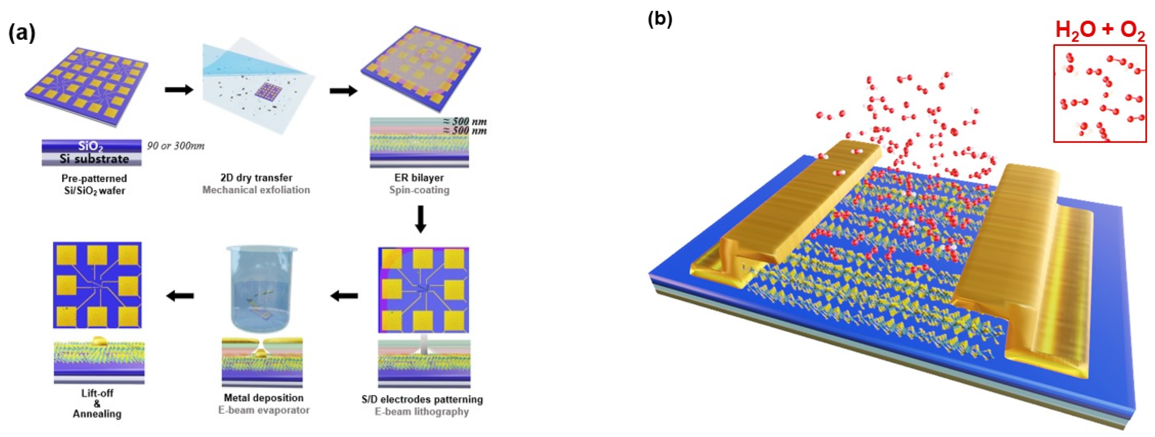
2.1. Fabrication of MoTe2 FETs

For back-gated MoTe2 device fabrication, a bulk 2H-MoTe2 (2D Semiconductors, Scottsdale, AZ, USA) thin film was mechanically exfoliated onto a boron-doped Si/90 nm-SiO2 substrate. The Si/SiO2 substrates were sonicated in acetone and isopropanol and then blown with N2 gas to dry the samples fully. To define the source and drain electrodes, electron beam lithography was performed following the spin-coating of e-beam resists (~1 μm, layers of copolymer EL 11/PMMA-C4, MicroChem, Westborough, MA, USA). Subsequently, a bilayer stack, i.e., 10 nm of nickel and 90 nm of gold, was deposited as contact metals using an e-beam evaporator at a rate of 0.005 kÅ/s. As the final step in the device fabrication, a lift-off process was performed in acetone and IPA solutions. The fabrication flow and the resultant device are illustrated in Figure 1a and Figure 1b respectively.

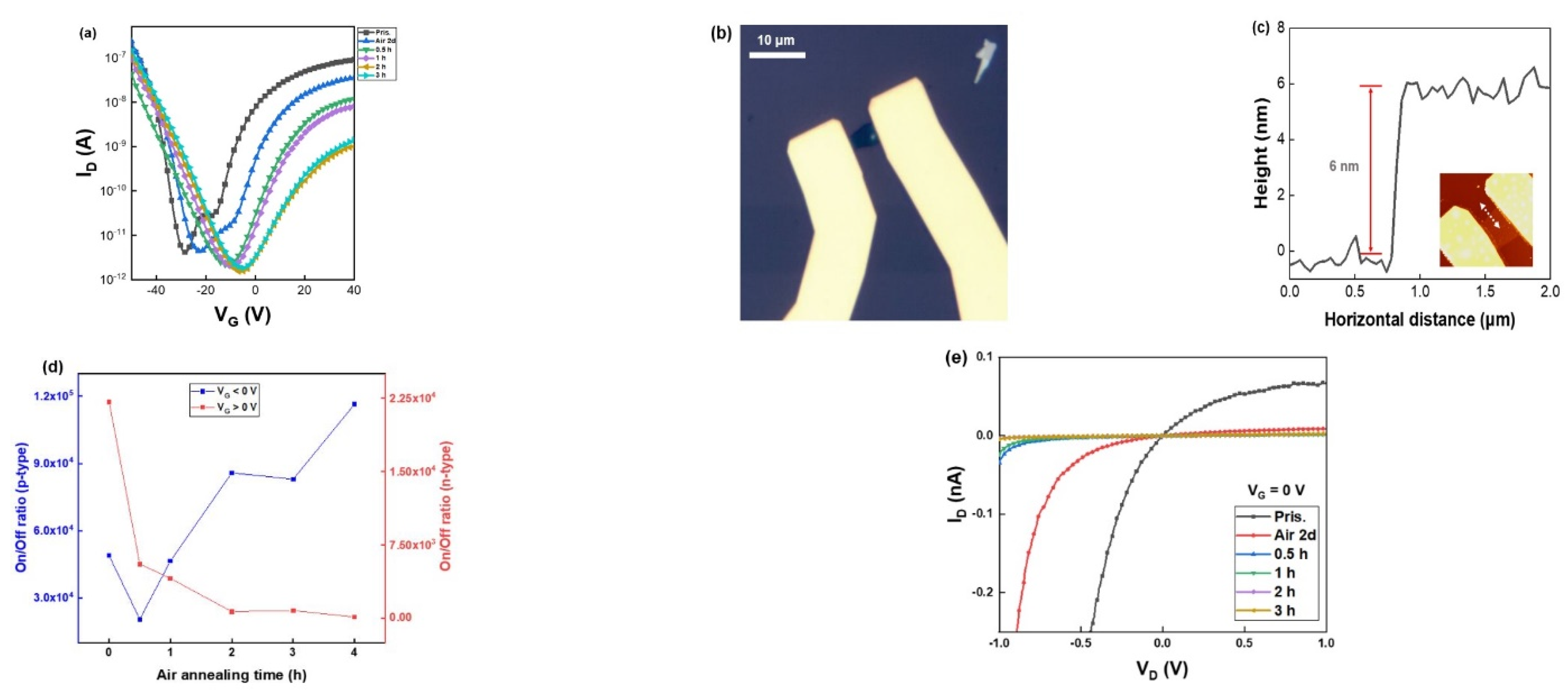
2.2. Air Annealing Process

The air annealing process was performed at a temperature of 100 °C on a hot plate to induce the hole-doping effect in the MoTe2 channel. The temperature was selected based on a previous study that investigated the doping effect at different temperature levels [27].

2.3. Oxygen Treatments

Oxygen plasma was induced on the MoTe2 flakes and devices at a pressure of 150 mTorr, an oxygen gas flow rate of 30 sccm, and a radio frequency power of 30 W for 20 min in a plasma chamber (CUTE, Femto Science, Hwaseong-si, Korea). Ultraviolet–ozone treatment was performed using Novascan PSDP-UVT under ambient conditions.

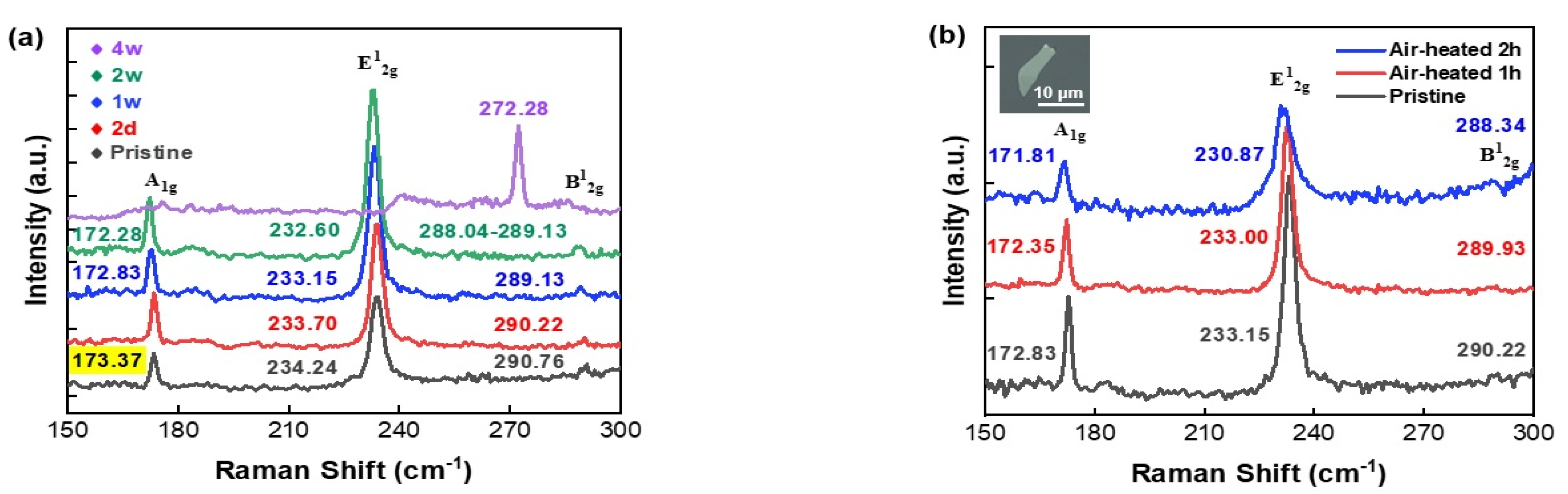
2.4. Characterisation of Thin Film and Device Performance

Raman spectroscopy was performed to investigate the semiconducting phase of MoTe2. All the Raman spectra were obtained using a Horiba Jobin Yvon LabRAM ARAMIS IR2 spectrometer with a 532 nm excitation laser, a laser power of 5 mW, and a laser spot of diameter 200 μm. The height profile of the channel was measured using an atomic force microscope (XE-100; Park Systems, Suwon-si, Korea). The electrical characterisations of the MoTe2 FETs were performed using a semiconductor parameter analyser (B1500A, Keysight, Santa Rosa, CA, USA). All the transfer characteristics were measured under a drain bias of 1 V.

3. Results and Discussion

Figure 2a shows the transfer curves of Device #1, whose optical image is shown in Figure 2b. The device initially behaves as an ambipolar transistor with a channel height of 6 nm (Figure 2c) and the smallest current, which corresponds to a charge neutrality condition of approximately −28 V. The device was first maintained under ambient conditions for two days to investigate the effect of air exposure without any treatment. It was then heated on a hot plate at 100 °C to induce oxygen adsorption on the surface, which led to a shift in Vth. As the air-heating time increased, the threshold voltages of the MoTe2 FETs, which were originally located in the negative gate bias regime, were consistently shifted in the positive direction. After 3 h of air annealing, the current on/off ratio improved from 4.89 × 10⁴ to 1.03 × 10⁵ and the charge neutrality point was nearest to zero. However, the SS also increased, which may be attributed to undesirable residual adsorption on the channel surface under ambient conditions. To investigate the effect of air heating alone precisely, each step of air heating was performed without rinsing in between. This can affect the pristine surface, which can lead to the deterioration of carrier mobility and an increase in SS. Therefore, the overall electrical performance appears to be degraded after a certain period of air heating owing to the long duration of exposure to ambient conditions (Supplementary Figure S1). However, a consistent hole-doping effect was observed in all the MoTe2 FETs, regardless of the channel profile. The shifting of the charge neutrality point shown in Figure 2 (Device #1) indicates that hole doping resulted from O2 molecules on the channel surface [6]. The oxygen/water redox couple adsorbed on the MoTe2 channel is known to cause electron transfer from MoTe2 to the redox couple, resulting in a p-doping effect [6,12].
The effect of air annealing can be compared to the plain air-exposure result. As shown in Figure 2a, after two days of air exposure, the transfer (Ids vs. Vgs) characteristics of the MoTe2 FET remained almost the same, with a slightly smaller current in the positive gate bias region and a small shift in the charge neutrality point to the p-side. As the air heating started, the transfer curve showed a smaller off current, resulting in a larger current on/off ratio, which was not observed in the air-exposed sample. An improvement in the on/off ratio continued to be observed, as shown in Figure 2d. After 2 h of air heating at 100 °C, the smallest current was observed at a gate voltage of −5 V. The output characteristics under a drain bias of 0 V without gate biasing showed that the device was turned on in the pristine state with a current flow of less than a few nanoamperes (Figure 2e). As the air heating proceeded, the current flow at zero gate bias gradually decreased and reached a few femtoamperes after 3 h of air heating. Ambipolar transistors have the limitation of intrinsically large off currents compared with unipolar transistors [28]. Our technique not only modifies the threshold regime but also rectifies the large off current issue in ambipolar MoTe2 devices.
While the device exhibited a significant positive shift in Vth by 23 V, the Nit value was not significantly affected, as it only changed from 1.91 × 1013 cm−2 eV−1 to 3.90 × 1013 cm−2 eV−1. The Nit was calculated using the following equation:
N it = SSlog e KT q 1 C ox q
where K is the Boltzmann constant, T is absolute temperature, q is elementary electron charge, and Cox is the oxide capacitance. The SS value is extracted from the maximum slope in the transfer characteristics.
Raman spectroscopy measurements of the freshly exfoliated multi-layered MoTe2 devices were obtained to investigate the changes in Raman modes after continuous air exposure and air heating to examine the effect of O2 molecules on MoTe2 with respect to molecular vibrations inside the material (Figure 3a,b). Under continual exposure to air, MoTe2 is strongly affected by defect sites resulting from O2 molecules [29]. Only a few reports have elucidated the effects of air exposure on MoTe2 [29] and MoTe2-based FETs [30]. Most studies on air-exposed 2D TMDs have been conducted on large-area chemically grown films rather than exfoliated flakes [31,32,33]. Figure 3 shows the three prominent Raman modes of MoTe2, each corresponding to the A1g, E12g, and B12g modes with 532 nm laser excitation. Changes in the three dominant peaks of MoTe2 after 2 days, 1 week, 2 weeks, and 4 weeks in chronological order are demonstrated. The in-plane (E12g) vibrational mode of the pristine state had a relatively higher energy than the out-of-plane (A1g) mode, indicating that the exfoliated MoTe2 is multi-layered [34]. As the air exposure time was increased, the E12g peaks exhibited gradual red shifts, revealing the p-doping effect from the adsorbed oxygen molecules on the surface. All three vibrational modes of the MoTe2 flakes exhibited red shifts, regardless of the intrinsic properties or thicknesses, indicating hole doping. The tendency of MoTe2 to transition towards p-type behaviour in air has been previously proven by density functional theory calculations and Kelvin probe force microscopy [35]. As depicted by the purple curve in Figure 3a, after a certain duration, major peaks of MoTe2 became undetectable due to undesirable adsorption of molecules besides oxygen. However, we inferred that the material remained physically intact since its peaks were all recovered from surface rinsing with toluene (Supplementary Figure S7), which is known to induce desorption of dopant molecules on surface channels [36]. The instability of air-exposure as a doping method can also be seen in device performance (Supplementary Figure S8).
Device #2 with a channel height of 6 nm also demonstrated a similar doping effect; after 2 h of air heating, Device #2 reached its neutral state with an improved current on/off ratio. After 2 h of air heating, the on/off ratio increased from 1.02 × 10⁴ to 1.28 × 10⁵. The charge neutrality point was observed at −21 V before air heating and at −5 V after 2 h of heating. After 6 h of air heating, the performance of Device #2 began to degrade significantly (Supplementary Figure S2). Both the on and off currents steeply increased with a significantly increased SS after that point. Device #3, made of an 8 nm-thick MoTe2 channel, also showed a similar trend under air heating; the smallest current, which was observed at −25 V in the as-fabricated state, was observed at a potential shift to the right by 20 V after 2 h of air heating, i.e., at a gate potential of −5 V. Moreover, the current on/off ratio constantly increased for up to 2 h of air heating owing to the continuously increasing on current. No significant changes were observed in the Nit and SS values, which revealed no significant electrical degradation. Nevertheless, after 2 h, the on currents at both the n- and p-sides began to decline. As shown in Supplementary Figure S3, the on/off ratio was on the order of 1 after 24 h of air heating, indicating a severe degradation in the switching performance. The Nit value also increased from 2.42 × 10¹³ to 1.17 × 10¹⁴ after 12 h of air heating. The transfer curves of Device #4 with a channel height of 15 nm depicted in Figure 4c reveal how the duration of air heating affects the electrical characteristics of the MoTe2 FET (results for up to 48 h are shown in Supplementary Figure S4). Based on the identical trend shown in the other devices, the charge neutrality point shifted by nearly 20 V in the positive direction after 2–3 h of air heating. The initial transfer curve shows more electron-dominant conduction behaviour because the MoTe2 channel is sufficiently thick at 13 nm, which is twice that of the other devices [37]. To drag the charge neutral point to 0 V, it appears that the duration of air heating must be at least 20 h. However, after 3 h, the on currents on both the n- and p-sides started to decrease gradually and the SS value began to increase, indicating a degraded switching performance. This pattern of increased SS and decreased on/off ratio values was once again observed in Device #4. The output characteristic curves in Figure 4d,e indicate that the device experienced a hole-doping effect owing to air annealing, showing a transition from ambipolar to p-type dominant behaviour. In Figure 4f, according to the trend in Figure 2e, the as-fabricated state of Device #4 was in the on state with a current flow of tens of nanoamperes and then the device transitioned to an off state after air annealing.

4. Conclusions

The air annealing approach to tailor the threshold of MoTe2 FETs presented in our study effectively induces a hole-doping effect, which yields a remarkable shift in transfer characteristics without causing a degradation in the device performance. Without the application of vacuum deposition or solution treatment to the transistor, which can deteriorate the overall electrical performance and require cumbersome post-processing, our method successfully demonstrates a precisely controlled doping effect via the strict control of the duration and temperature of air heating.

Supplementary Materials

The following are available online at https://www.mdpi.com/article/10.3390/app12083840/s1, Figure S1: Transfer curves of MoTe2 Device #1, Figure S2: Transfer curves of MoTe2 Device #2, Figure S3: Transfer curves of MoTe2 Device #3, Figure S4: Transfer curves of MoTe2 Device #4, Figure S5: Output curves (Ids−Vds) of Device #1 under zero gate bias, Figure S6: Raman spectra of air-heated MoTe2 Device #2, Figure S7: Raman spectra of toluene treated, air-exposed MoTe2 flake, Figure S8: Transfer Characteristics curves of as-fabricated (dark grey) and air-exposed for 1-month (blue) MoTe2 FET, Figure S9: Transfer Characteristics curves of MoTe2 FET air heated at 150 °C, Figure S10: Raman Spectra of air heated MoTe2 flake over a range 150–110 cm−1 (inset: optic image), Figure S11: (a) Transfer curves and (b) AFM height profile (inset: AFM image) of MoTe2 FET #5.

Author Contributions

Conceptualisation, S.K. and H.S.; methodology, S.K. and Y.R.; formal Analysis, S.K. and H.S.; investigation, S.K. and Y.C.; resources, H.S. and B.-K.J.; data curation, H.S. and A.H.J.; writing—original draft preparation, S.K.; writing—review and editing, S.K. and Y.R.; supervision, H.S. and B.-K.J.; funding acquisition, B.-K.J. All authors have read and agreed to the published version of the manuscript.

Funding

This study was supported by the Brain Korea 21 Project in 2022 and Samsung Electronics Co., Ltd. (No. IO201214-08159-01).

Institutional Review Board Statement

Not applicable.

Conflicts of Interest

The authors declare no conflict of interest.

References

  1. Chu, T.; Ilatikhameneh, H.; Klimeck, G.; Rahman, R.; Chen, Z. Electrically Tunable Bandgaps in Bilayer MoS2. Nano Lett. 2015, 15, 8000–8007. [Google Scholar] [CrossRef] [PubMed]
  2. Lee, W.H.; Park, Y.D. Tuning Electrical Properties of 2D Materials by Self-Assembled Monolayers. Adv. Mater. Interfaces 2018, 5, 170036. [Google Scholar] [CrossRef]
  3. Jiang, J.; Zheng, Z.; Guo, J. Tuning the hysteresis voltage in 2D multilayer MoS2 FETs. Phys. B Condens. Matter 2016, 498, 76–81. [Google Scholar] [CrossRef]
  4. Rani, A.; Dicamillo, K.; Khan, A.H.; Paranjape, M.; Zaghloul, M.E. Tuning the polarity of MoTe2 fets by varying the channel thickness for gas-sensing applications. Sensors 2019, 19, 2551. [Google Scholar] [CrossRef] [PubMed]
  5. Geng, H.; Yuan, D.; Yang, Z.; Tang, Z.; Zhang, X.; Yang, K.; Su, Y. Graphene van der Waals heterostructures for high-performance photodetectors. J. Mater. Chem. C 2019, 7, 11056–11067. [Google Scholar] [CrossRef]
  6. Liu, J.; Wang, Y.; Xiao, X.; Zhang, K.; Guo, N.; Jia, Y.; Zhou, S.; Wu, Y.; Li, Q.; Xiao, L. Conversion of Multi-layered MoTe2 Transistor Between P-Type and N-Type and Their Use in Inverter. Nanoscale Res. Lett. 2018, 13, 291. [Google Scholar] [CrossRef]
  7. Sun, L.; Ding, M.; Li, J.; Yang, L.; Lou, X.; Xie, Z.; Zhang, W.; Chang, H. An Investigation in Phase Transition of MoTe2 Film with Continuous Tellurization Reaction. In Proceedings of the IOP Conference Series: Materials Science and Engineering, Kazimierz Dolny, Poland, 21–23 November 2019; Volume 677. [Google Scholar]
  8. Si, C.; Choe, D.; Xie, W.; Wang, H.; Sun, Z.; Bang, J.; Zhang, S. Photoinduced Vacancy Ordering and Phase Transition in MoTe2. Nano Lett. 2019, 19, 3612–3617. [Google Scholar] [CrossRef]
  9. Cheong, H.; Cheon, Y.; Lim, S.Y.; Kim, K. Structural phase transition and interlayer coupling in few-layer 1t′ and td mote2. ACS Nano 2021, 15, 2962–2970. [Google Scholar] [CrossRef]
  10. Chi, Z.; Chen, H.; Zhao, Q.; Weng, Y.X. Ultrafast carrier and phonon dynamics in few-layer 2H-MoTe2. J. Chem. Phys. 2019, 151, 114704. [Google Scholar] [CrossRef]
  11. Tan, Y.; Luo, F.; Zhu, M.; Xu, X.; Ye, Y.; Li, B.; Wang, G.; Luo, W.; Zheng, X.; Wu, N.; et al. Controllable 2H-to-1T′ phase transition in few-layer MoTe2. Nanoscale 2018, 10, 19964–19971. [Google Scholar] [CrossRef]
  12. Aguirre, C.M.; Levesque, P.L.; Paillet, M.; Lapointe, F.; St-Antoine, B.C.; Desjardins, P.; Martel, R. The role of the oxygen/water redox couple in suppressing electron conduction in field-effect transistors. Adv. Mater. 2009, 21, 3087–3091. [Google Scholar] [CrossRef]
  13. Wang, Q.; Chen, J.; Zhang, Y.; Hu, L.; Liu, R.; Cong, C.; Qiu, Z.J. Precise layer control of MoTe2 by Ozone treatment. Nanomaterials 2019, 9, 756. [Google Scholar] [CrossRef] [PubMed]
  14. Qu, D.; Liu, X.; Huang, M.; Lee, C.; Ahmed, F.; Kim, H.; Ruoff, R.S.; Hone, J.; Yoo, W.J. Carrier-Type Modulation and Mobility Improvement of Thin MoTe2. Adv. Mater. 2017, 29, 1606433. [Google Scholar] [CrossRef] [PubMed]
  15. Iqbal, M.W.; Elahi, E.; Amin, A.; Aftab, S.; Aslam, I.; Hussain, G.; Shehzad, M.A. A facile route to enhance the mobility of MoTe2 field effect transistor via chemical doping. Superlattices Microstruct. 2020, 147, 106698. [Google Scholar] [CrossRef]
  16. Lim, J.Y.; Pezeshki, A.; Oh, S.; Kim, J.S.; Lee, Y.T.; Yu, S.; Hwang, D.K.; Lee, G.H.; Choi, H.J.; Im, S. Homogeneous 2D MoTe2 p–n Junctions and CMOS Inverters formed by Atomic-Layer-Deposition-Induced Doping. Adv. Mater. 2017, 29, 1701798. [Google Scholar] [CrossRef]
  17. Luo, W.; Zhu, M.; Peng, G.; Zheng, X.; Miao, F.; Bai, S.; Zhang, X.A.; Qin, S. Carrier Modulation of Ambipolar Few-Layer MoTe2 Transistors by MgO Surface Charge Transfer Doping. Adv. Funct. Mater. 2018, 28, 1704539. [Google Scholar] [CrossRef]
  18. Liang, Q.; Gou, J.; Arramel; Zhang, Q.; Zhang, W.; Wee, A.T.S. Oxygen-induced controllable p-type doping in 2D semiconductor transition metal dichalcogenides. Nano Res. 2020, 13, 3439–3444. [Google Scholar] [CrossRef]
  19. Liu, X.; Qu, D.; Yuan, Y.; Sun, J.; Yoo, W.J. Self-Terminated Surface Monolayer Oxidation Induced Robust Degenerate Doping in MoTe2for Low Contact Resistance. ACS Appl. Mater. Interfaces 2020, 12, 26586–26592. [Google Scholar] [CrossRef]
  20. Park, J.Y.; Bae, H.; Moon, D.I.; Jeon, C.H.; Choi, Y.K. Threshold voltage tuning technique in Gate-All-Around MOSFETs by utilizing gate electrode with potential distribution. IEEE Electron Device Lett. 2016, 37, 1391–1394. [Google Scholar] [CrossRef]
  21. Van, N.H.; Lee, J.H.; Sohn, J.I.; Cha, S.; Whang, D.; Kim, J.M.; Kang, D.J. Tunable threshold voltage of an n-type Si nanowire ferroelectric-gate field effect transistor for high-performance nonvolatile memory applications. Nanotechnology 2014, 25, 205201. [Google Scholar] [CrossRef]
  22. Kirsch, P.D.; Sivasubramani, P.; Huang, J.; Young, C.D.; Quevedo-Lopez, M.A.; Wen, H.C.; Alshareef, H.; Choi, K.; Park, C.S.; Freeman, K.; et al. Dipole model explaining high-k /metal gate field effect transistor threshold voltage tuning. Appl. Phys. Lett. 2008, 92, 092901. [Google Scholar] [CrossRef]
  23. Li, M.; Lin, C.Y.; Chang, Y.M.; Yang, S.H.; Lee, M.P.; Chen, C.F.; Lee, K.C.; Yang, F.S.; Chou, Y.; Lin, Y.C.; et al. Facile and Reversible Carrier-Type Manipulation of Layered MoTe2Toward Long-Term Stable Electronics. ACS Appl. Mater. Interfaces 2020, 12, 42918–42924. [Google Scholar] [CrossRef] [PubMed]
  24. Choi, M.S.; Lee, M.; Ngo, T.D.; Hone, J.; Yoo, W.J. Chemical Dopant-Free Doping by Annealing and Electron Beam Irradiation on 2D Materials. Adv. Electron. Mater. 2021, 7, 2100449. [Google Scholar] [CrossRef]
  25. Iqbal, M.W.; Amin, A.; Kamran, M.A.; Ateeq, H.; Elahi, E.; Hussain, G.; Azam, S.; Aftab, S.; Alharbi, T.; Majid, A. Tailoring the electrical properties of MoTe2 field effect transistor via chemical doping. Superlattices Microstruct. 2019, 135, 106247. [Google Scholar] [CrossRef]
  26. Vasdev, A.; Kamboj, S.; Sirohi, A.; Mandal, M.; Marik, S.; Singh, R.P.; Sheet, G. Field induced hysteretic structural phase switching and possible CDW in Re-doped MoTe2. J. Phys. Condens. Matter 2021, 33, 255401. [Google Scholar] [CrossRef] [PubMed]
  27. Ke, Y.; Qi, D.; Han, C.; Liu, J.; Zhu, J.; Xiang, Y.; Zhang, W. Facile p-Doping of Few-Layer MoTe2 by Controllable Surface Oxidation toward High-Performance Complementary Devices. ACS Appl. Electron. Mater. 2020, 2, 920–926. [Google Scholar] [CrossRef]
  28. Torricelli, F.; Ghittorelli, M.; Smits, E.C.P.; Roelofs, C.W.S.; Janssen, R.A.J.; Gelinck, G.H.; Kovács-Vajna, Z.M.; Cantatore, E. Ambipolar Organic Tri-Gate Transistor for Low-Power Complementary Electronics. Adv. Mater. 2016, 28, 284–290. [Google Scholar] [CrossRef] [PubMed]
  29. Chen, B.; Sahin, H.; Suslu, A.; Ding, L.; Bertoni, M.I.; Peeters, F.M.; Tongay, S. Environmental changes in MoTe2 excitonic dynamics by defects-activated molecular interaction. ACS Nano 2015, 9, 5326–5332. [Google Scholar] [CrossRef]
  30. Wang, S.P.; Zhang, R.J.; Zhang, L.; Feng, L.F.; Liu, J. Accurate change of carrier types within ultrathin MoTe2 field-effect transistors with the time exposed to ambient air. J. Mater. Sci. 2019, 54, 3222–3229. [Google Scholar] [CrossRef]
  31. Chae, S.H.; Jin, Y.; Kim, T.S.; Chung, D.S.; Na, H.; Nam, H.; Kim, H.; Perello, D.J.; Jeong, H.Y.; Ly, T.H.; et al. Oxidation effect in octahedral hafnium disulfide thin film. ACS Nano 2016, 10, 1309–1316. [Google Scholar] [CrossRef]
  32. Gao, J.; Li, B.; Tan, J.; Chow, P.; Lu, T.M.; Koratkar, N. Aging of Transition Metal Dichalcogenide Monolayers. ACS Nano 2016, 10, 2628–2635. [Google Scholar] [CrossRef]
  33. Park, J.H.; Vishwanath, S.; Wolf, S.; Zhang, K.; Kwak, I.; Edmonds, M.; Breeden, M.; Liu, X.; Dobrowolska, M.; Furdyna, J.; et al. Selective Chemical Response of Transition Metal Dichalcogenides and Metal Dichalcogenides in Ambient Conditions. ACS Appl. Mater. Interfaces 2017, 9, 29255–29264. [Google Scholar] [CrossRef] [PubMed]
  34. Grzeszczyk, M.; Gołasa, K.; Zinkiewicz, M.; Nogajewski, K.; Molas, M.R.; Potemski, M.; Wysmołek, A.; Babiñski, A. Raman scattering of few-layers MoTe2. 2D Mater. 2016, 3, 025010. [Google Scholar] [CrossRef]
  35. Stan, G.; Ciobanu, C.V.; Likith, S.R.J.; Rani, A.; Zhang, S.; Hacker, C.A.; Krylyuk, S.; Davydov, A.V. Doping of MoTe2 via Surface Charge Transfer in Air. ACS Appl. Mater. Interfaces 2020, 12, 18182–18193. [Google Scholar] [CrossRef] [PubMed]
  36. Kim, S.; Kim, C.; Hwang, Y.H.; Lee, S.; Choi, M.; Ju, B.K. Carrier-type modulation of tungsten diselenide (WSe2) field-effect transistors (FETs) via benzyl viologen (BV) doping. Chem. Phys. Lett. 2021, 770, 138453. [Google Scholar] [CrossRef]
  37. Rani, A.; DiCamillo, K.; Krylyuk, S.; Davydov, A.V.; Debnath, R.; Taheri, P.; Korman, C.E.; Paranjape, M.; Zaghloul, M.E. Control of Polarity in Multilayer MoTe2 Field-Effect Transistors by Channel Thickness. In Low-Dimensional Materials and Devices 2018; International Society for Optics and Photonics: San Diego, CA, USA, 2018. [Google Scholar]
Figure 1. (a) Fabrication flow for FET devices and (b) schematic illustration of MoTe2 FET.
Applsci 12 03840 g001
Figure 2. (a) Transfer curves (at VD = 1 V), (b) optical image, (c) AFM height profile (inset: AFM image), (d) current on/off ratios versus air annealing time, and (e) output curves (at VG = 0 V) of MoTe2 FET #1.
Applsci 12 03840 g002
Figure 3. Raman spectra of (a) MoTe2 in air exposure and (b) MoTe2 under air heating.
Applsci 12 03840 g003
Figure 4. Transfer curves of (a) Device #2, (b) Device #3, and (c) Device #4 and output curves of Device #2: (d) as fabricated, (e) after air annealing for 2 h, and (f) at VG = 0 V.
Applsci 12 03840 g004
Publisher’s Note: MDPI stays neutral with regard to jurisdictional claims in published maps and institutional affiliations.

