Article

Modelling of a Resonant Charging Circuit for a Solid-State Marx Generator

Karlsruhe Institute of Technology, 76344 Eggenstein-Leopoldshafen, Germany
*
Author to whom correspondence should be addressed.
Appl. Sci. 2022, 12(23), 12481; https://doi.org/10.3390/app122312481
Submission received: 28 October 2022 / Revised: 28 November 2022 / Accepted: 2 December 2022 / Published: 6 December 2022
(This article belongs to the Special Issue Advances in Solid-State Pulsed Power Applications)

Abstract

:
For the pulsed electric field treatment of plant material on an industrial scale, Marx-type pulse modulators are used as a pulse source. The combination of a conventional Marx generator design equipped with solid-state switches with the concept of resonant charging via current-compensated chokes enables the set-up of a Marx generator having only one active semiconductor switch per stage. Thereby, the pulse shape is defined by the passive components of the RLC-pulse circuit. In the course of the design of such a resonant charging circuit, common-mode current components through the current-compensated chokes need to be considered. Moreover, especially for a generator having its ground connection at its centre, induced voltages versus ground need to be addressed. Therefore, an investigation based on circuit simulations has been made. The simulations showed that the common-mode current components decay to zero just after the resonant charging process and cause a voltage transient at the terminal of the power supply, which needs to be floating versus ground. In order to reduce the amplitude of this transient, the effects of adding a damping resistor have been studied. However, adding this resistor may involve an increase in the common-mode current components. Moreover, the common-mode current components of different chokes are influenced by the on-time of the switches. In the paper, based on the simulation results, different operation modes with and without the damping resistor are discussed. Thereby, the on-time of the switches has been varied. Selected simulation results have been verified by means of measurements.

1. Introduction

For the pulsed electric field treatment of plant cells, pulses with voltages in the range of several 10 kV and currents in the order of at least several 100 A are required. Thereby, the Marx circuit is one of the common configurations for the pulse generator [1]. A basic pulse circuit for one stage of a Marx-type solid-state pulse generator for the generation of unipolar pulses comprises a capacitor, a solid-state switch, and a free-wheeling diode. After closing the switch, the capacitor delivers its stored energy into the connected load. The energy transfer ends if either the complete stored energy has been transferred to the load or the switch has been opened. In the case of an inductive component of the impedance of the attached load, the current may commutate to the current path through the free-wheeling diode. If the switch has previously opened, this prevents the occurrence of an over-voltage across the switch.
This basic circuit can be stacked. The charging path can be set up using solid-state switches comprising additional active switches [2]. When charging the stage capacitors in a parallel configuration, the power supply needs to have the characteristic of a current source in order to provide direct control of the charging current.
The Marx generator features voltage multiplication according to the number of stages and the voltage stress of each component to be limited to the stage voltage only [3]. Both advantages are achieved by the combination of charging the capacitors in a parallel configuration and discharging them in a series configuration, and, moreover, by adding circuit elements, i.e., inductors or resistors, in between the stages providing a DC current flow during charging and transient insulation during pulse generation. This concept has been varied, in particular with respect to the arrangement of the current path for charging. In [4,5], pulse circuits with voltage multiplication and resonant charging are described. Both circuits feature circuit elements, i.e., diodes and transformers, providing the required insulation between stages during pulse generation, which are stressed with a pulse voltage which is significantly higher than the stage voltage. Article [6] describes a charging circuit featuring a voltage source with a series resistor and some diodes, which bridge several stages and, hence, need to block more than only the stage voltage. In [7], a pulse transformer is used for distributing the gate signals to the generator’s IGBT switches, which needs to be designed to insulate the peak pulse voltage. According to [8], a boost converter configuration acting as a current source and delivering a bipolar output voltage delivers current to the charging path, which is equipped with diodes and MOSFET switches designed to block the stage voltage only.
The goal of the investigations described in this paper is to set up a Marx generator with resonant charging and a design with only one actively controlled switch per stage in order to reduce the effort for control circuitry with respect to designs having more active switches per stage. Moreover, this combination allows advantageously for a fine-tuning of the charging voltage using only the single switch per stage in addition to its original use as a pulse switch.
The pulse shape can be determined by means of appropriate control of the pulse switches allowing for the generation of arbitrary voltage shapes. Such an operation requires stage capacitors, which are sufficiently large to keep the voltage droop during pulse generation small and, hence, allow the generation of almost rectangular voltage shapes. If the controlled variation of the pulse shape is not important, the pulse shape can be determined by the passive circuit elements of the pulse circuit. In the case of the classic Marx generator, this would be an RLC circuit.
The pulse circuit of such an electroporation device comprises the Marx generator, the treatment chamber, and the circuit inductance. The Marx generator serves as capacitance. Thereby, the effective capacitance C is formed by the series configuration of the stage capacitors Cstage as given in Equation (1) and depends on the number of stages n.
C = C s t a g e n
The treatment chamber comprises an electrode system for the pulsed electric field applied to the processed material. It can be modelled as an ohmic resistance R. The inductance L can either be formed by the stray inductance of the pulse circuit only or augmented by a coil added to the pulse circuit. The resistance of the treatment chamber may vary with the electric conductivity of the processed material, which depends, among other parameters, on the temperature and the filling factor. As a consequence, the pulse shape may vary.
The solution of the differential Equation (2)
v C t + R C · v ˙ C t + L C · v ¨ C t = 0
for the initial conditions v C 0 = V 0 and v ˙ C 0 = 0   V s describes the time characteristic of the voltage across the Marx generator’s effective capacitance C. The voltage across the resistance R of the treatment chamber, v R t (Equations (3)–(5)), can be derived according to [9]. Thereby, three different cases are distinguished depending on the quality factor Q as given in Equation (6):
Aperiodic case (Q < 0.5):
v R t = R V 0 L R 2 4 L 2 1 L C e R 2 L · t sinh R 2 4 L 2 1 L C · t
Critically damped case (Q = 0.5):
v R t = R V 0 L · t · e R 2 L · t
Damped periodic case (Q > 0.5):
v R t = R V 0 L 1 L C R 2 4 L 2 e R 2 L · t sin 1 L C R 2 4 L 2 · t
with
Q = 1 R · L C
with the voltage across the resistance R of the treatment chamber, v R t , the pulse current ip(t) can be calculated according to Equation (7).
i p t = 1 R · v R t
For the pulsed electric field treatment of biological material, a pulse shape similar to the aperiodically damped case or the strongly damped periodic case of an RLC circuit is already in use in industrial-scale electroporation devices equipped with Marx generators [2]. Therefore, for the new generator design, a Marx-type generator with solid-state switches and an RLC pulse circuit serving as a conventional pulse-forming circuit has been chosen. However, the free-wheeling diodes as part of the pulse generator topology prevent the stage capacitors from being charged in reverse polarity in the case of an oscillatory waveform of the pulse. In this case, as soon as the stage capacitors are discharged, the current driven by the circuit inductance commutates into the free-wheeling diodes and from that moment on, the pulse current decays exponentially, governed by the time constant τ of the resulting LR circuit.
τ = L R
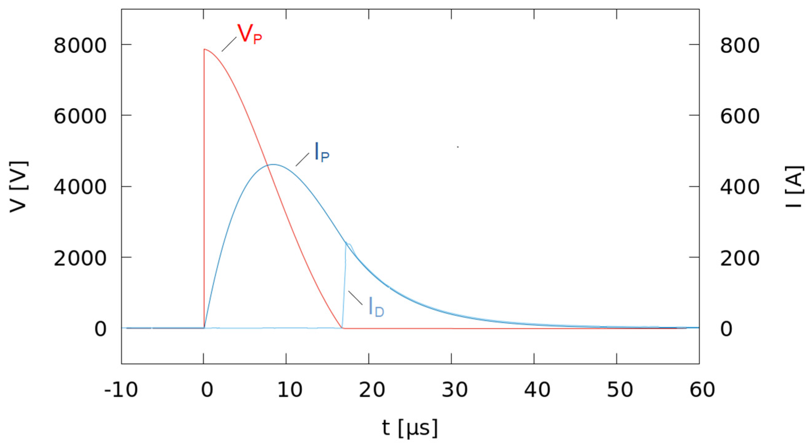
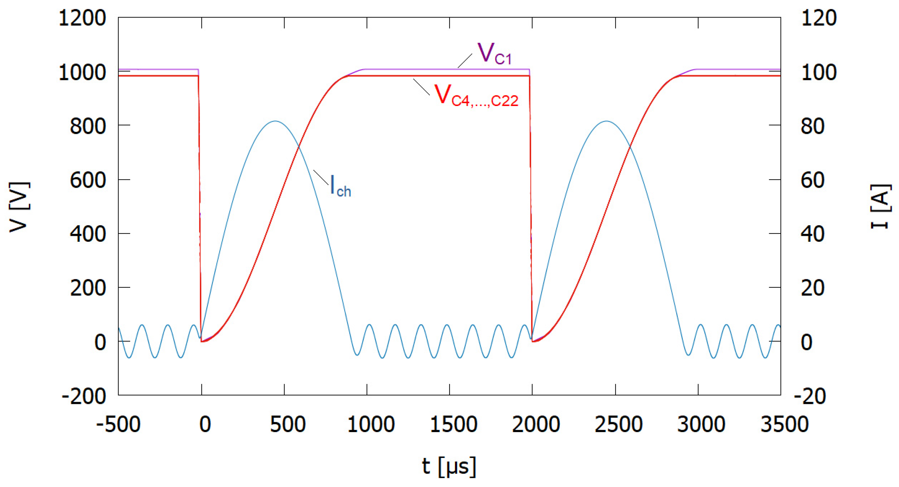
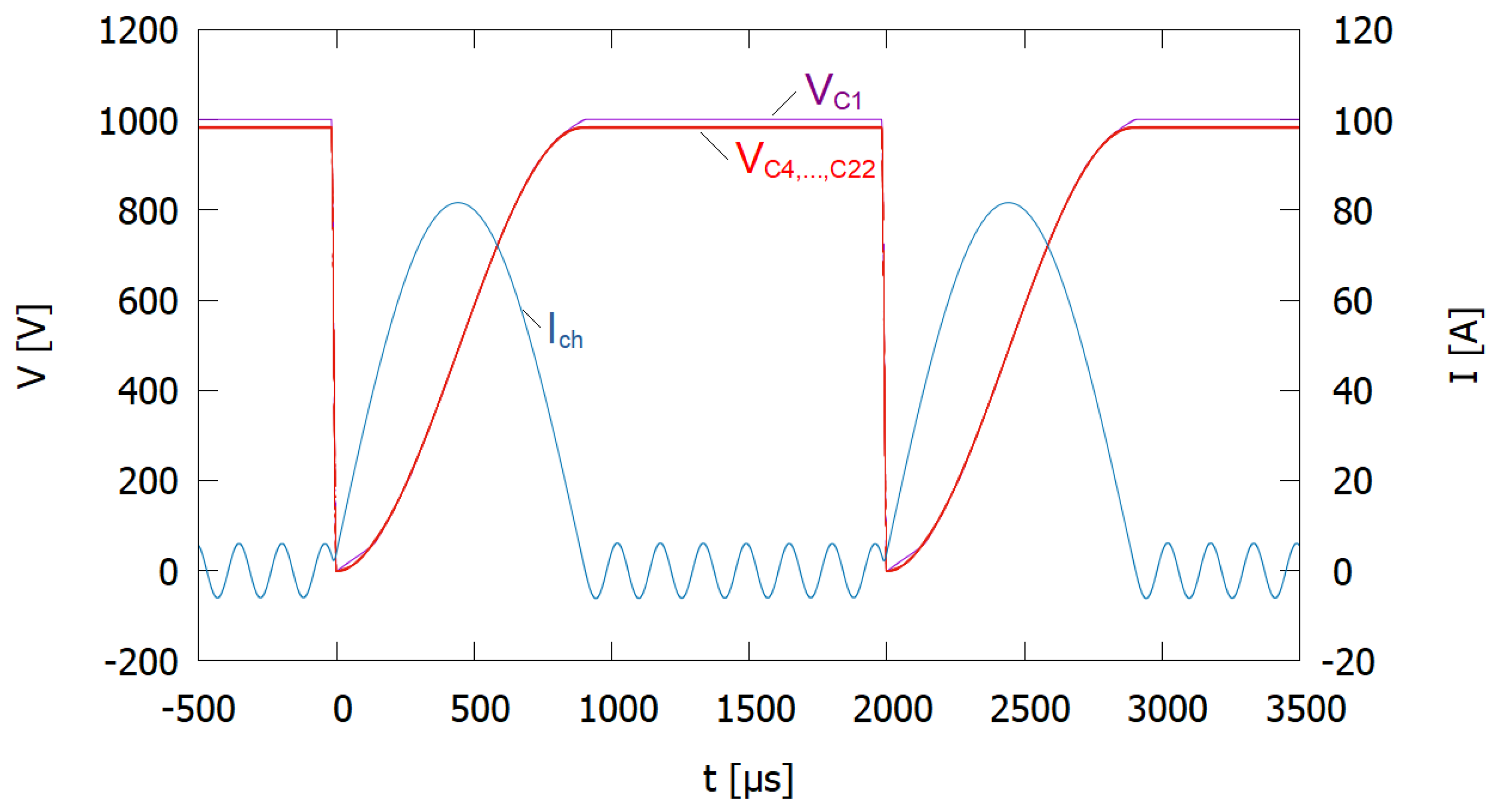
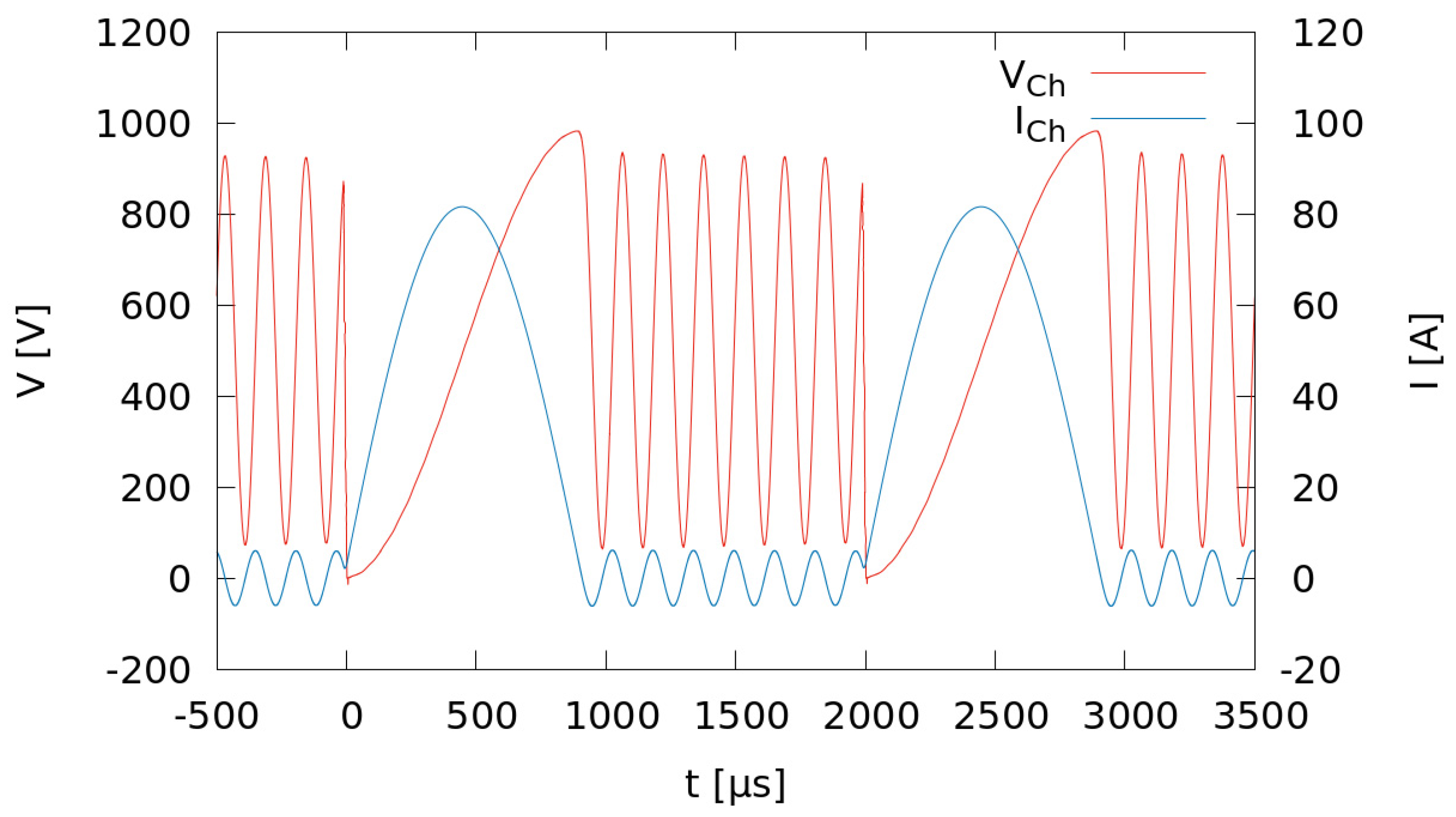
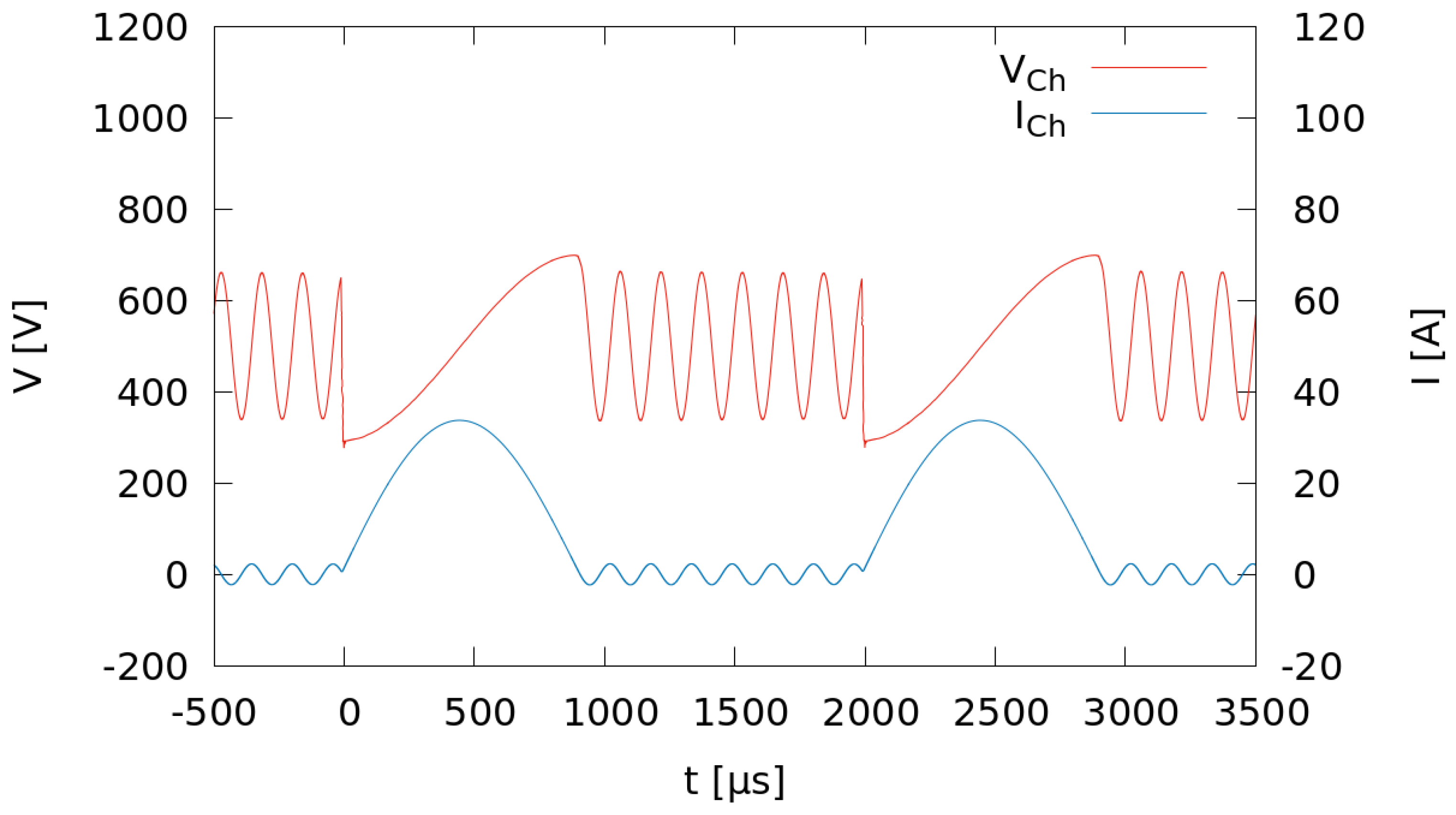
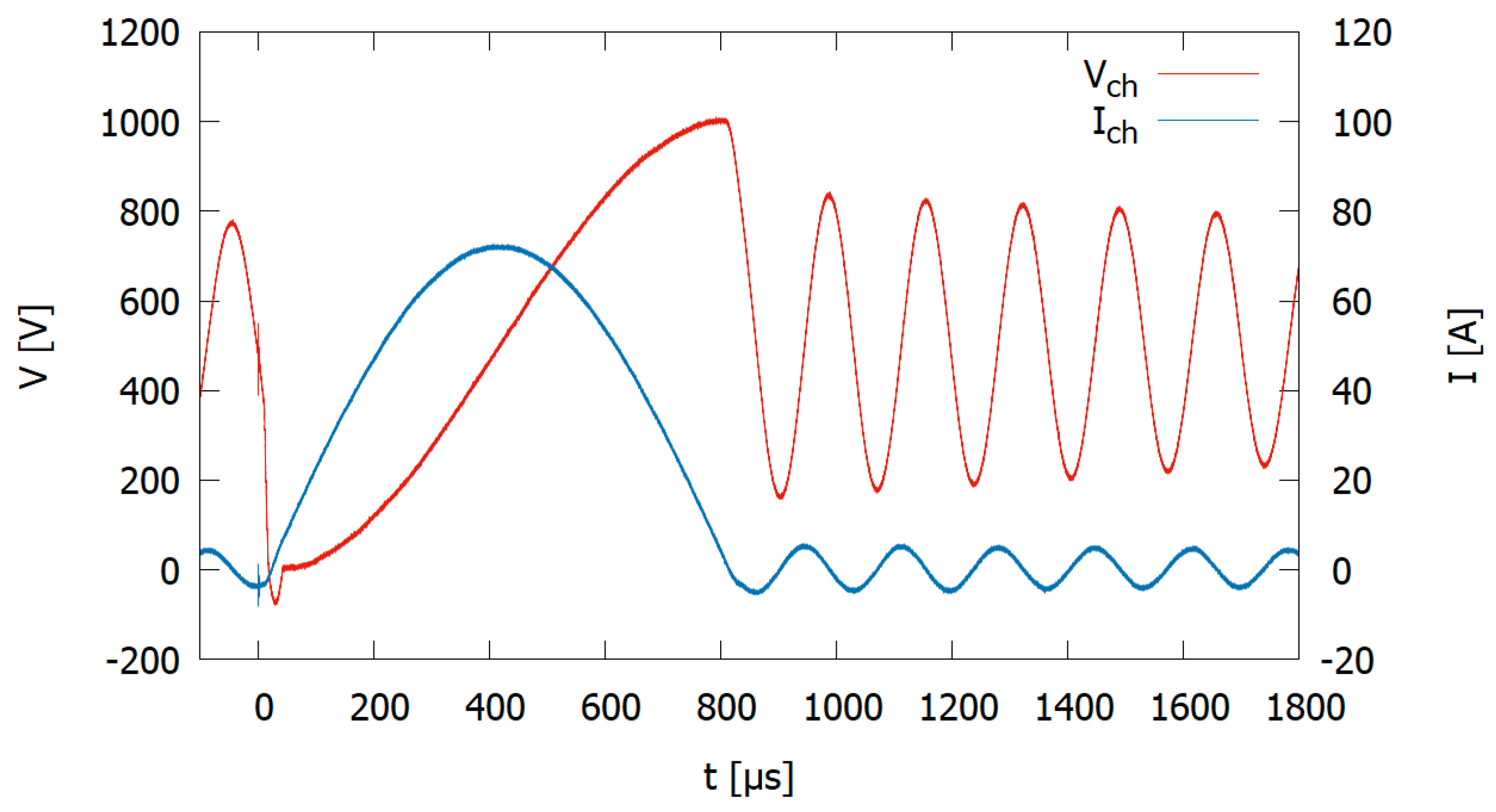
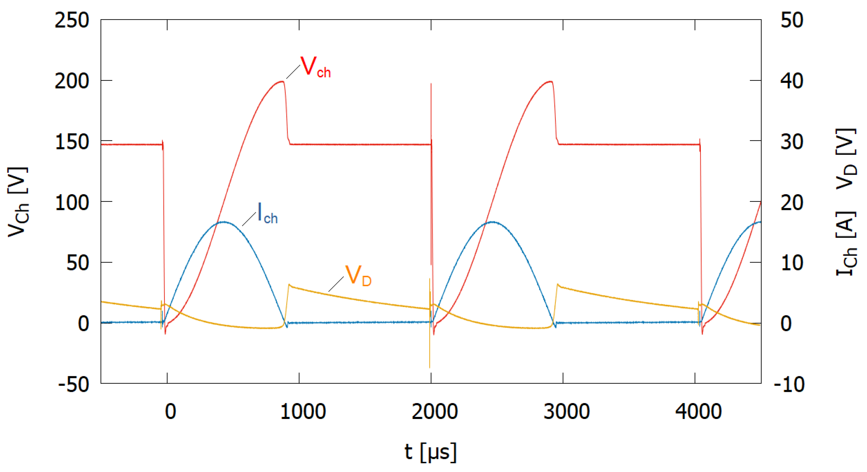
Figure 1 shows the simulated pulse voltage VP and pulse current IP at the output terminal of an 8-stage Marx generator with free-wheeling diodes. After the discharge of the stage capacitors, the pulse current commutates to the free-wheeling diodes (ID).
For such a design, a conventional charging circuit equipped with charging coils can be used. However, when operating such a pulse generator at a higher pulse repetition rate and as a consequence, the product of pulse length and pulse repetition rate becomes larger, using current-compensated chokes instead of the charging coils is advantageous for enabling fast charging [2]. Current-compensated chokes feature a low inductivity during charging, as they are operated in differential mode. During pulse generation, their high inductivity under common-mode conditions serves well for transient stage insulation.
The design based on current-compensated chokes in the charging path can be combined with a power supply having the characteristic of a voltage source and an additional inductance between the power supply and the Marx generator to enable resonant charging of the generator [10].
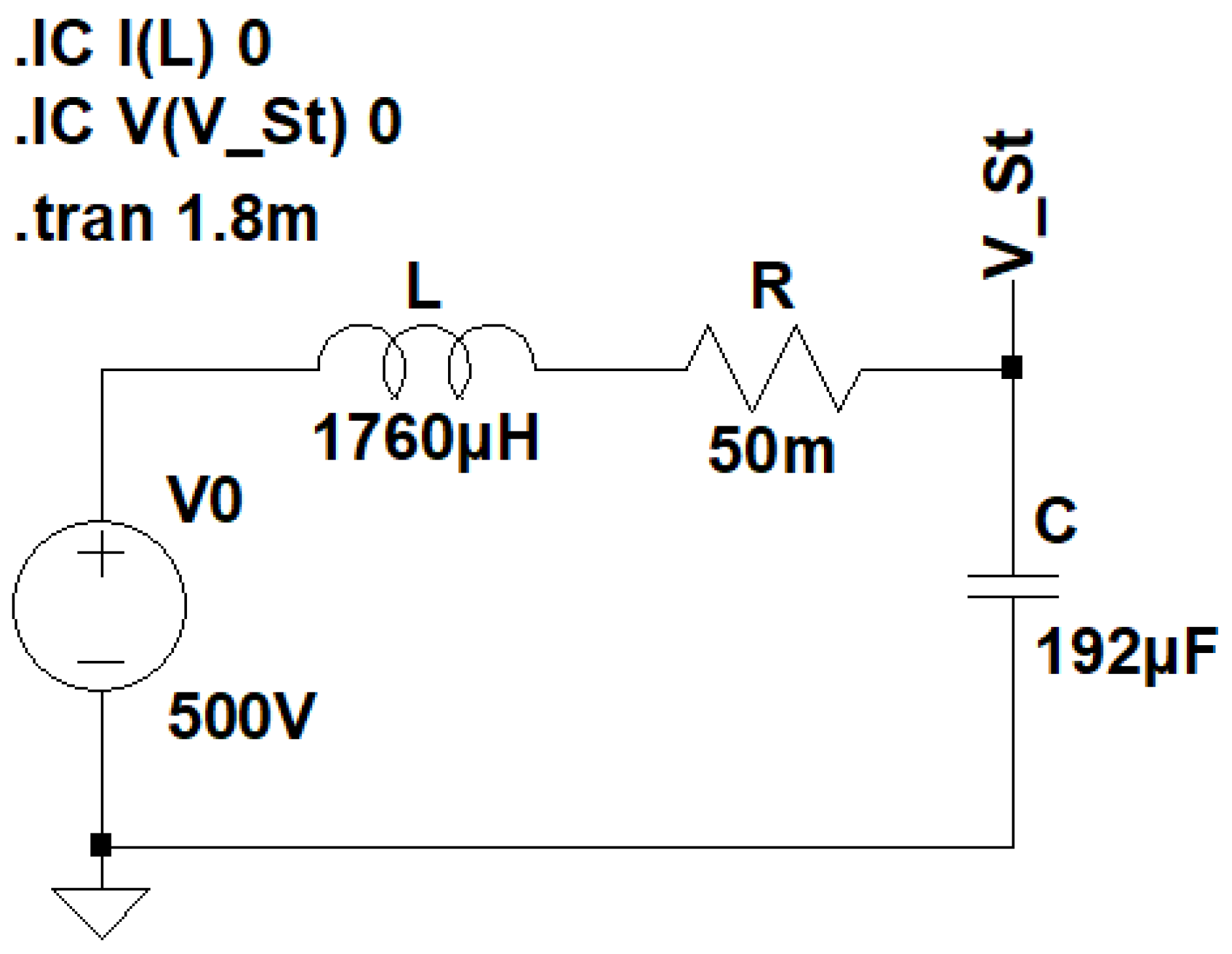
Figure 2 shows a simplified circuit for basic studies on resonant charging. The voltage source V0 supplies energy to the circuit. The capacitance C represents the parallel connection of the generator’s stage capacitors. The inductance L forms together with the capacitance C a resonant circuit. The resistance R represents the resistive losses of the circuit. Initially, the capacitance C is uncharged, and there is no current flow through L, i.e., i(0) = 0. So, there is no energy stored in the circuit. Charging ends when the voltage across the capacitance C reaches its peak value.
The solution of the differential Equation (9)
v C t + R C · v ˙ C t + L C · v ¨ C t = 0
for the initial conditions v C 0 = 0 and v ˙ C 0 = i 0 C = 0   V s describes the time characteristic of the voltage across the paralleled stage capacitors C for the case of a circuit being initially free of energy. Thereby, depending on the value of the quality factor Q according to Equation (6), three different cases (Q < 0.5, Q = 0.5, and Q > 0.5) might be considered. However, for efficient charging, the losses represented by R need to be low. Therefore, only the oscillatory case with Q > 0.5 is of interest. The voltage across the stage capacitors is given by
v C t = V 0 1 e R 2 L · t   cos 1 L C R 2 4 L 2 · t + 1 4 L R 2 C 1 sin 1 L C R 2 4 L 2 · t
If the resistance R is assumed to be zero, the voltage v C t rises up to a peak value of 2 · V 0 . Hence, for such a design, during repetitive operation, the charging voltage of the stage capacitors may reach approximately twice that of the supplying voltage source. Thereby, the initial condition v C 0 = 0 is guaranteed by a complete discharge of the stage capacitors during the previous pulse. If the initial condition for the current through the inductance L is modified in such a way, that there is already a significant energy WL stored in L, which correlates to an initial current
i 0 = 2 W L L   ,
The initial condition for v ˙ C 0 becomes
v ˙ C 0 = i 0 C = 1 C 2 W L L
The initial current of the charging process, i(0), rises with an extended on-time of the stage switches. As long as these switches are closed, the stage capacitors are shorted, and the current through the inductance L rises according to
i t = V 0 R 1 e R L t .  
However, if the value of the resistance R is negligibly small, the rise of the current i(t) can be approximated to be in proportion to the time according to
i t V 0 L · t
The opening of the switches defines the beginning of the charging process as described above. Thereby, the charging voltage can be fine-tuned by means of a modulation of the on-time of the stage switches.
An industrial-scale electroporation device can be designed for an operation around one well-defined operating point. If there is no need for a wide variation of the voltage, the rectified voltage across a DC-link capacitor grounded at its negative pole may serve as a cheap voltage source. An additional transformer may provide the required insulation from the grid.
In order to investigate the operation of the resonant charging circuit of a solid-state switched Marx circuit via current-compensated chokes, circuit simulations of an eight-stage Marx circuit have been performed.

2. Materials and Methods

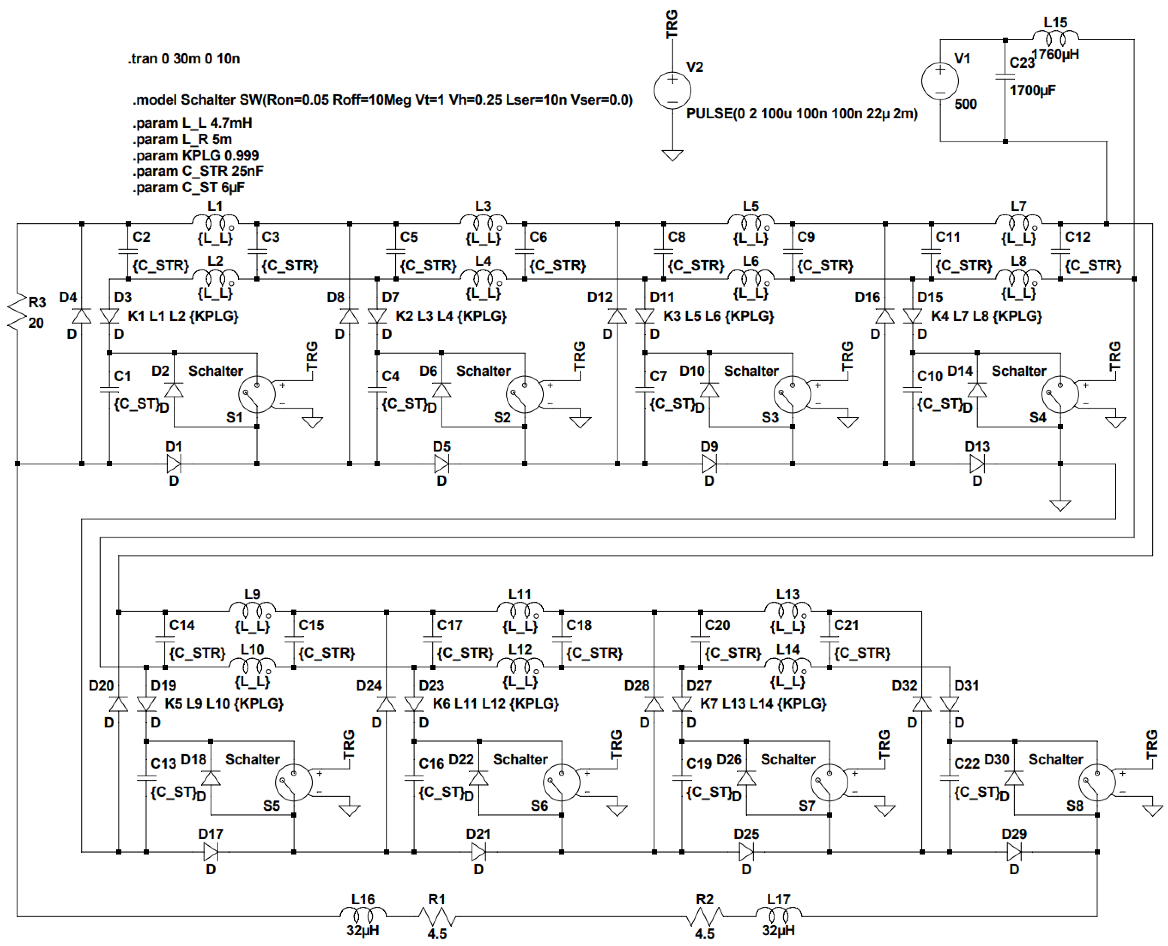
For the circuit simulation of an 8-stage Marx generator, a circuit model for circuit simulation using the software LTspice [11] has been set up, which is shown in Figure 3. Based on the circuit topology and component values, LTspice sets up a system of difference equations and solves them numerically for a sequence of adapted time steps considering the appropriate initial conditions. In between the time steps, linear interpolation is applied [11]. LTspice has also been used for post-processing, i.e., the calculation of data, which has been derived from the original simulation data, such as, e.g., the integration over time or averaging of a curve.
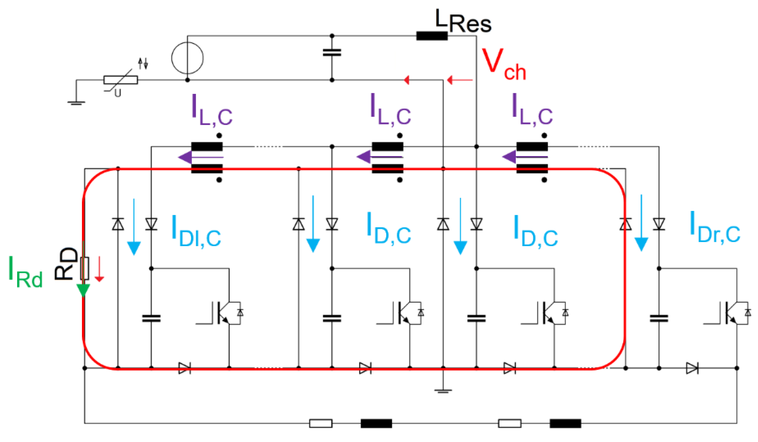
Each stage is represented by its stage capacitor having the capacitance C_ST = 6 µF, and the solid-state switch, which is modelled using a voltage-controlled switch and an anti-parallel diode representing the internal diode co-packed with many IGBT switches. Additionally, each stage features a bypass diode (D1, D5, D9, D13, D17, D21, D25, and D29 in Figure 3). The load is modelled as a combined resistive and inductive load (R1 + R2, L16 + L17). The charging path comprises the coupled inductor-pairs (L1, L2), (L3, L4) … (L13, L14), each representing one current-compensated choke. The capacitance between both windings is represented by the sum of the adjacent capacitors (C2 + C3) … (C20 + C21). Each winding has an inductance of LL = 4.7 mH and resistance of 
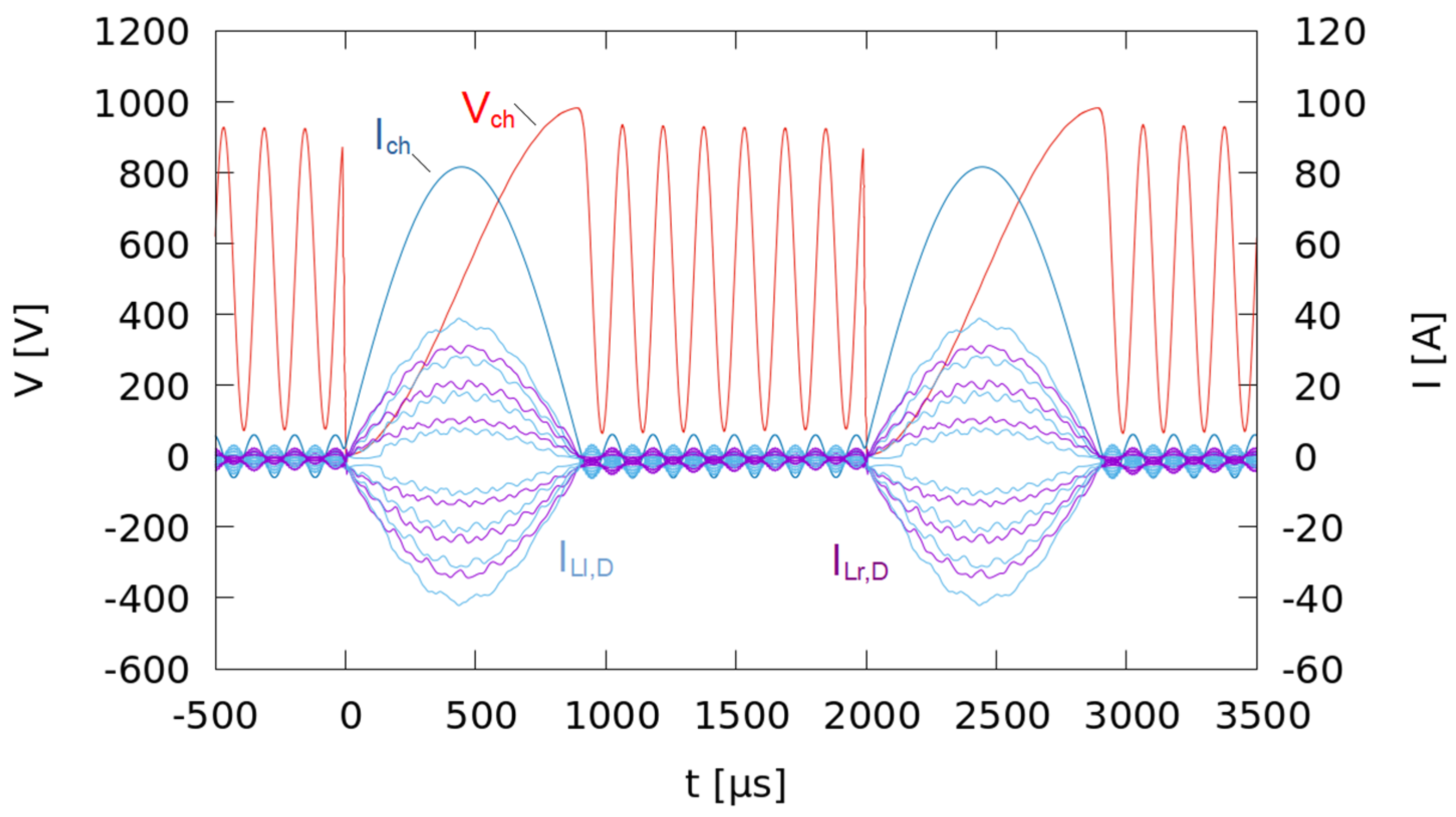
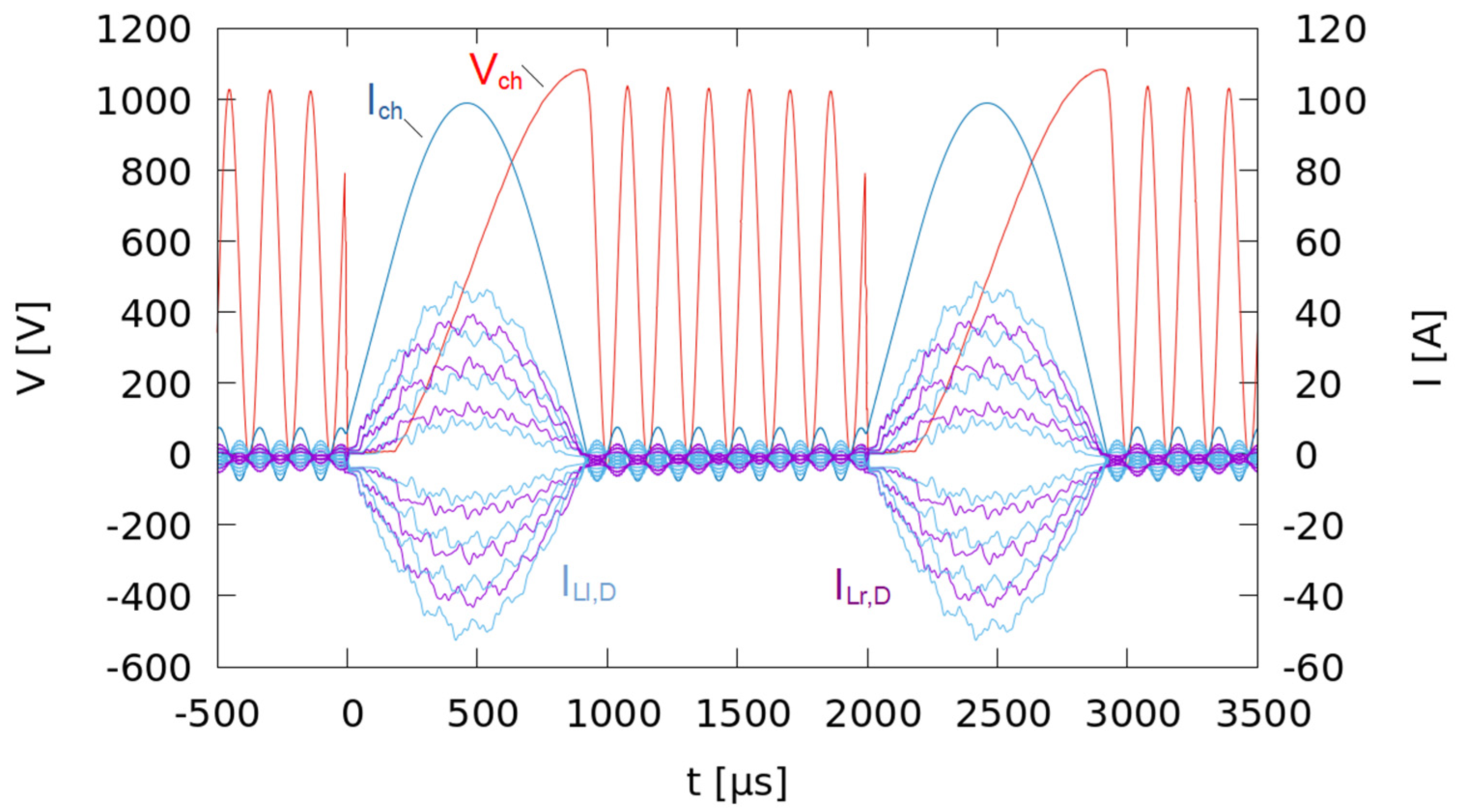
LR = 5 mΩ. With a coupling coefficient of KPLG = 0.999, very well magnetic coupling between both windings has been assumed. The common-mode current component through one current-compensated choke is obtained by calculating the difference of the currents through both windings. The stages are connected to the charging path via diodes (D3, D4), (D7, D8) … (D31, D32). These diodes prevent the stage capacitors from discharging via the charging path after resonant charging.
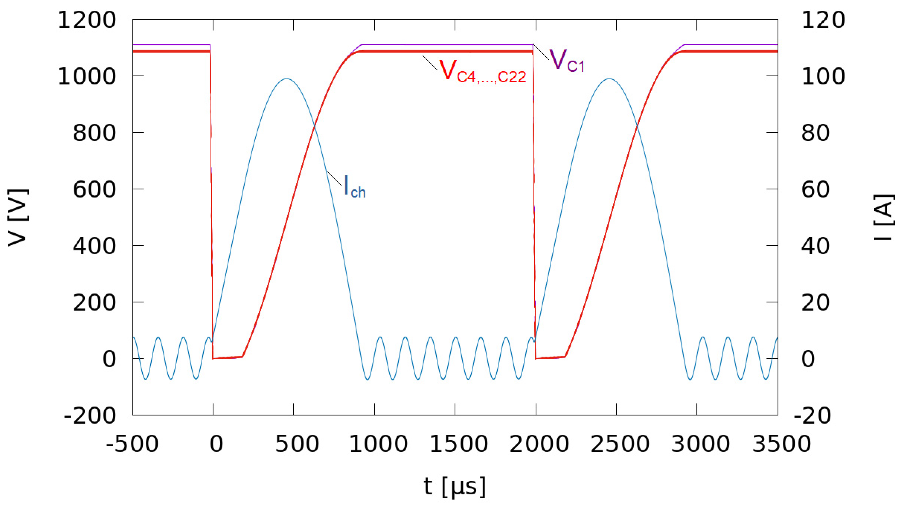
The voltage source needed for the resonant charging circuit is modelled by the ideal voltage source V1. The voltage source V1 is paralleled with a capacitance C23 serving in a real setup as a DC-link capacitor. However, for the simulation, this capacitor is not required.
The inductance L15 forms, together with the paralleled stage capacitors, the resonant circuit for resonant charging. Just after pulse generation, the stage capacitors are discharged completely. The bypass diodes of each stage prevent the stage capacitors from being charged at the opposite polarity and, hence, prevent the pulse circuit from oscillating. As soon as the voltage of the stage capacitors falls below the voltage of the power supply, the charging current starts to rise and recharges the stage capacitors in a parallel arrangement. Thereby, the voltage across the stage capacitors reaches approximately twice the voltage of the feeding voltage source.
The values of the stage capacitors, the load, the current-compensated chokes, and the inductance L15 have been selected based on a design for a solid-state Marx generator with a stage voltage of 1 kV delivering pulses with an approximate pulse length th = 10 µs at a pulse repetition rate of up to 500 Hz to the load. Thereby, the pulse length is measured at half amplitude, and the average power of one stage operating at 1 kV and 500 Hz is 1.5 kW [10,12,13].
In order to generate an output voltage, which is symmetric to ground potential, the pulse generator is grounded at its centre. This arrangement is of advantage for a later connection of a pulsed electric field treatment chamber [14]. The power supply for charging the generator is isolated to ground potential. During the operation of the real circuit, a varistor may limit the voltage versus ground in case of an over-voltage event.
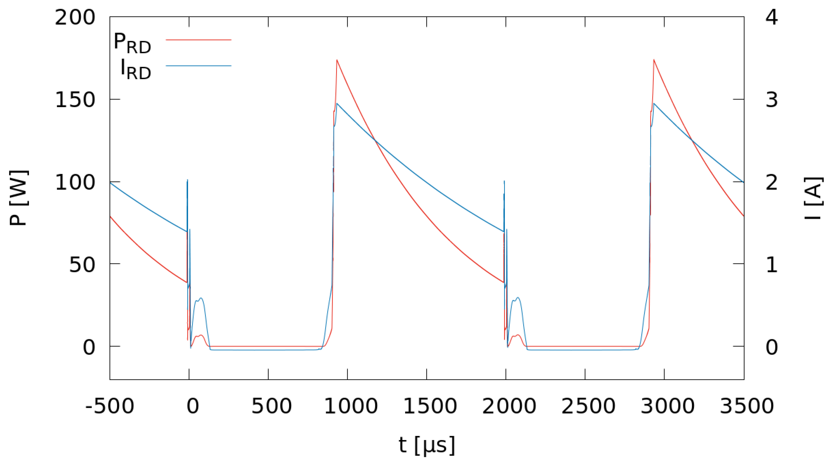
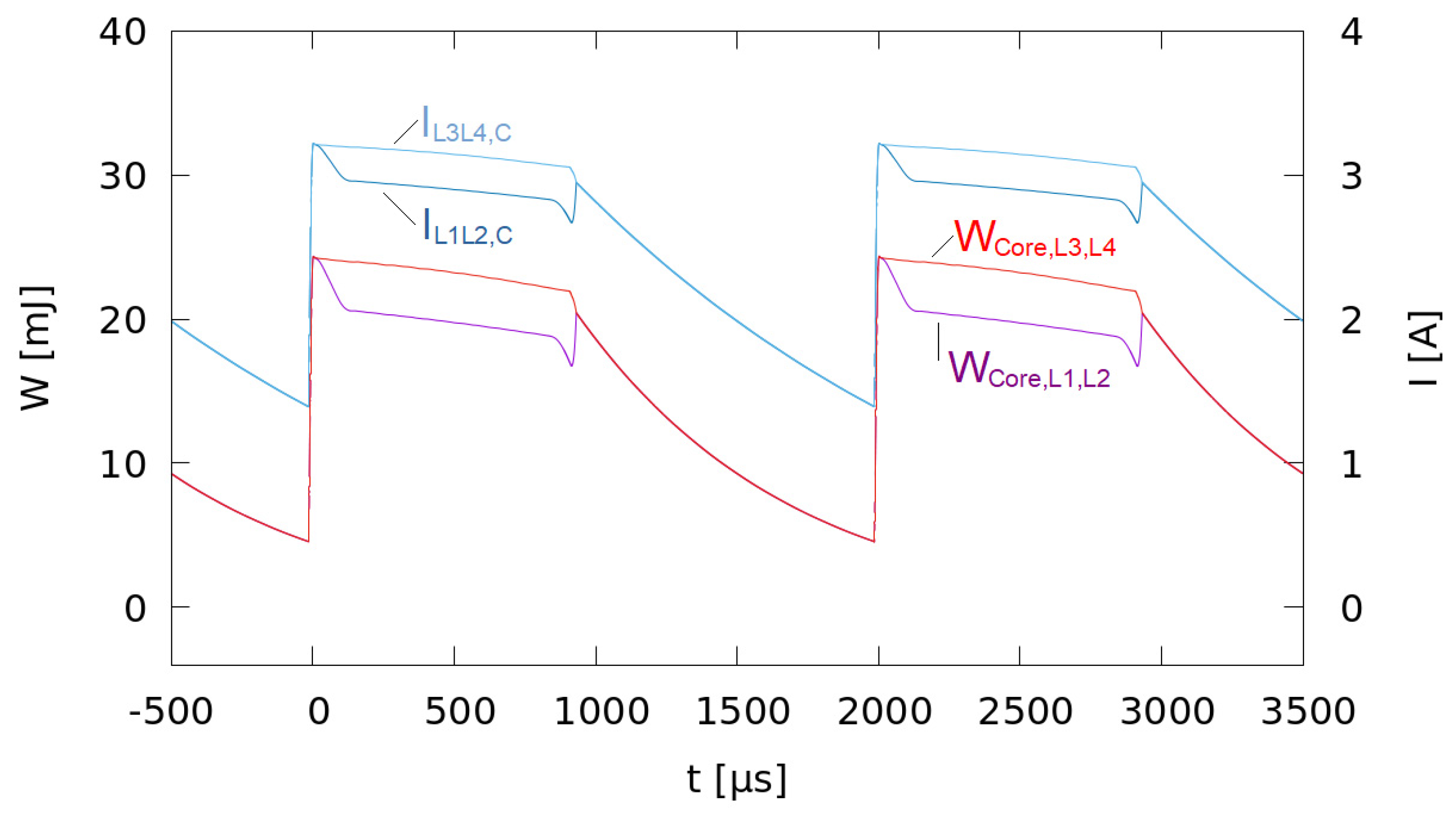
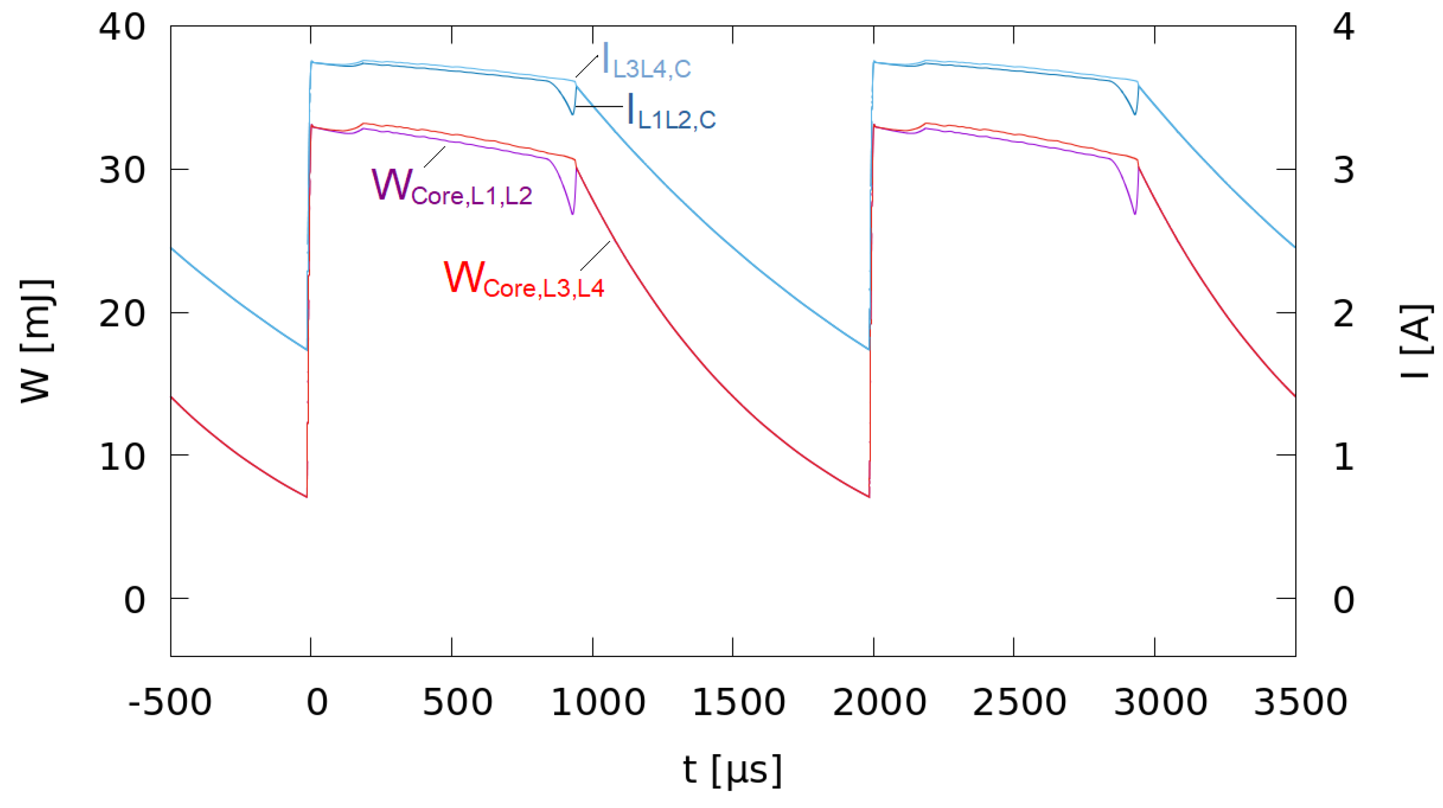
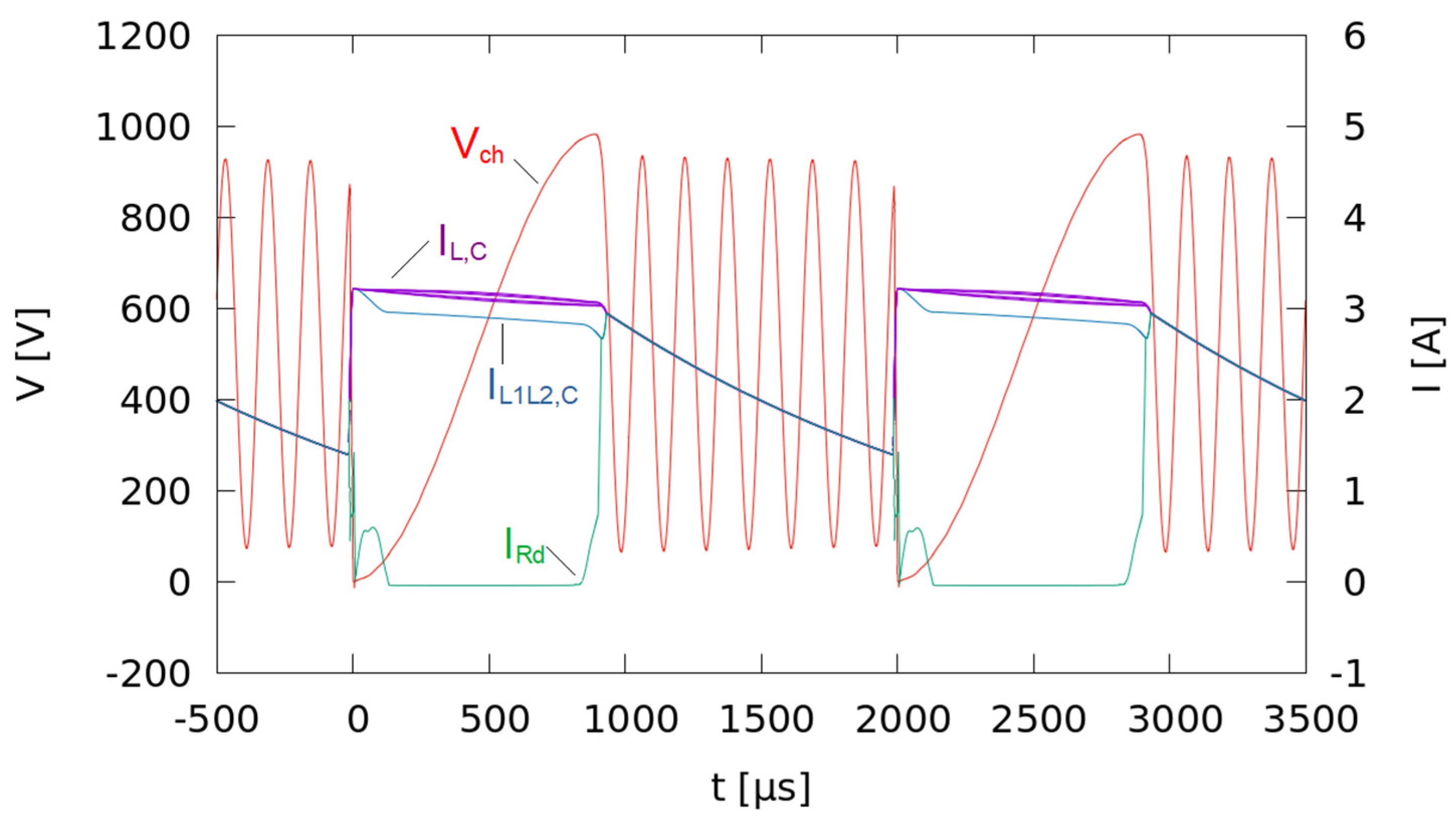
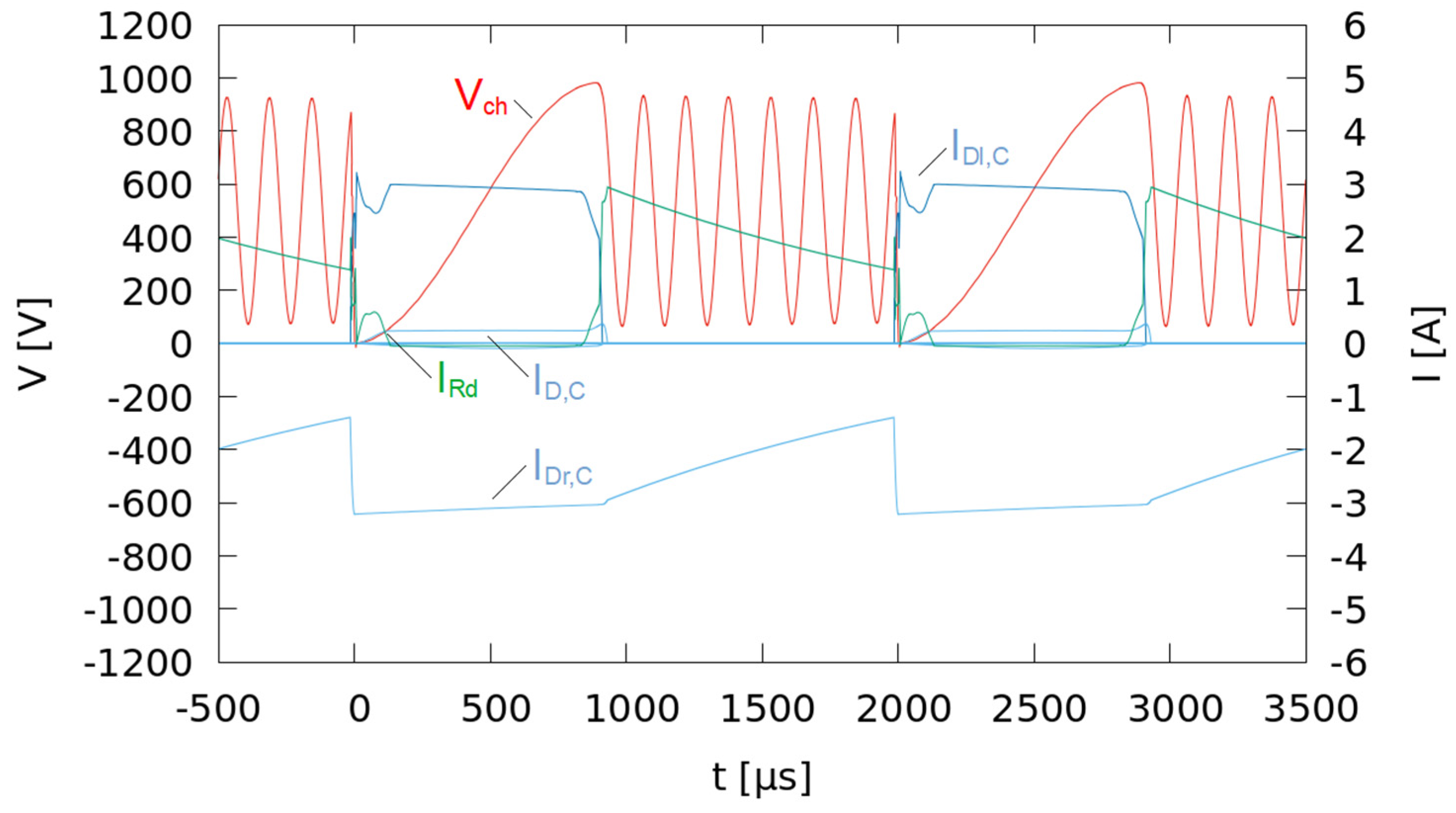
During pulse generation, some amount of magnetic energy is stored in the chokes resulting in a common-mode current. An accumulation of such energy from pulse to pulse and, hence, an increase in the common-mode current may cause the saturation of the magnetic cores resulting in a loss of inductance. If the common-mode current is interrupted suddenly, an induced voltage may result in an over-voltage causing excessive stress on the insulation. In order to dissipate some of the energy accumulated in the current-compensated chokes between two pulses, a damping resistor RD (R3 in Figure 3) has been implemented. It has been added to the circuit in such a way that it is not part of the current path during the charging process and, hence does not cause additional losses during charging.
For the simulations, the value of the damping resistor R3 and the on-time of the switches have been varied, and the effects on the circuit have been studied.

3. Results

3.1. Operation without Damping Resistor RD

A straightforward way of operating the Marx generator is to omit the damping resistor RD. In order to investigate this mode of operation, the resistor RD, which corresponds to the resistor R3 in the simulation model according to Figure 3, has been modelled as an open circuit. Figure 4 shows the voltages at the positive charging path of the current-compensated chokes versus the ground potential and the voltage of the ground-side connection of the power supply. Just after charging has ended, magnetic energy, which has been stored in the current-compensated chokes due to the previous pulse generation, causes a voltage pulse. The voltage rises from stage to stage, starting with the rightmost stage and reaches almost the level of the charging voltage at the leftmost stage. As a consequence, the voltage at the ground-side terminal of the power supply (VL9,G) in the centre of the Marx generator is shifted to a considerable voltage of approximately 400 V. This voltage amplitude needs to be taken into account when designing the insulation of the power supply versus ground. In the diagram in Figure 4, the voltage VL9,G is highlighted in violet colour.
Figure 5 displays the voltages across the stage capacitors C1, C4, C7, C10, C13, C16, C19, and C22 according to Figure 3, together with the generator’s charging current Ich. The charging process of the capacitor of the leftmost stage (C1) continues after the charging process of the other stage capacitors has already ended.
Figure 6 shows the voltages across the series configuration of the stage capacitor and the diode connecting the charging path to its positive terminal, together with the voltages across the diodes in the return path for the charging current. When the charging current through the charging inductance LRes, ICh, ceases, the voltage across the series configuration of D3 and C1 (VD3,C1) still rises. Hence, the charging of the stage capacitor of the leftmost stage still continues. In Figure 6, VD3,C1 is shown in red colour. The energy stored in the current-compensated chokes is transferred to the stage capacitor C1 of the leftmost stage. Thereby, the current path comprises the stages’ bypass diodes D1, D5, D9 … D25, and the diode D32. The voltage across D32 (VD32) is almost zero, as it is conducting within the considered time frame. In Figure 6, it is highlighted in violet colour. The voltages across the remaining diodes in the return path for the charging current are positive, so the diodes block due to the voltages induced in the ground-side coils of the current-compensated chokes. On its way back, the current passes the current compensated chokes.
Figure 7 shows the energy stored in the cores of the leftmost and its neighbouring current-compensated choke and as well as the respective common-mode currents through both. The common-mode currents through both current-compensated chokes and, hence, the energies stored in the cores differ. Current and energy of the leftmost choke are lower. After each charging process, the common-mode current and the energy stored in the cores decay to zero for all chokes.

3.2. Adaptation of the Damping Resistor RD

With a damping resistor of almost no resistance, damping is poor, and an accumulation of magnetic energy in the cores of the current-compensated chokes can be expected. Figure 8 shows the simulated common-mode currents in the charging path for the first five pulses. The common-mode current rises stepwise from pulse to pulse. As a consequence, the cores of the current-compensated chokes will be driven into saturation.
In order to achieve a considerable amount of damping, a value of 20 Ohm has been selected. This choice has been made based on simulations.
Figure 9 shows the voltages across the stage capacitors for the case of RD equal to 20 Ohm. The results are similar to the corresponding results achieved without RD, as shown in Figure 4. Again, the charging process of the capacitor of the leftmost stage (C1) continues after the charging process of the other stage capacitors has already ended.
Figure 10 shows the simulation results of the charging voltage VCh and the charging current ICh, both derived from the charging input terminal of the generator, the voltage Viso across D20, and the voltage VD across the damping resistor RD (=R3). The voltage VD does not decay to zero between two pulses. However, the magnetic energy in the current-compensated chokes is sufficiently low in order to prevent the core from saturation. The simulation shows that the pulse generator operates under steady-state conditions. Thereby, the voltage Viso across D20 is much lower than in the case without a damping resistor, as shown in Figure 4 (VL9,G). However, some energy stored in the current-compensated chokes dissipates in RD instead of being re-used for additional charging of the leftmost stage. Figure 11 shows the power and the current at RD. The average power is 50.3 W. Figure 12 shows the energy stored in the cores of the leftmost and its neighbouring current-compensated choke and the common-mode currents through both. When a part of the energy stored in the chokes is dissipated by RD, in the considered case, the reduction of the stored energy is 15.8 mJ per choke, so the average power delivered by one choke into RD when operating at a pulse repetition rate of 500 Hz is 7.85 W. Summing up over all seven current-compensated chokes of the circuit results in a total average power of 55.0 W, which fits well to the average power at RD. The remaining losses of approximately 5 W are distributed among the other components of the circuit.

3.3. Modulation of the On-Time

Modulation of the on-time of the IGBT switches enables some control of the charging voltage per stage. The influence of the on-time of the IGBT switches on the charging voltage has been studied based on the circuit model. Figure 13 and Figure 14 show two simulation results of the charging voltage and the charging current, both derived from the charging input terminal of the generator, with an on-time of 22 µs and 200 µs, respectively. The inductive energy, which is initially stored in the charging coil before the beginning of the resonant charging, varies with the on-time. Charging of the stage capacitor is delayed until the solid-state switches open. In the case of a longer on-time of the switches, the stage capacitors are charged to a higher voltage. Hence, the modulation of the on-time can be used for fine-tuning the charging voltage. In the case of an on-time of 22 µs, the stages are charged to a peak voltage of 1 kV. Thereby, the on-time of 22 µs is slightly longer than it would be required for pulse generation only. Hence, some additional energy is stored in the charging coil L15, just sufficient to compensate for the losses and to reach exactly twice the source voltage of 500 V. However, when opening the switches, the charging current is still small compared to the pulse current. So, the switches operate almost under soft-switching conditions. For an on-time of 200 µs, a charging voltage of 1.1 kV per stage is obtained. As long as the switches are closed, the current through L15 rises almost linearly. Figure 15 shows the energy stored in the cores of the leftmost and its neighbouring current-compensated choke and the common-mode currents through both for an on-time of the solid-state switches of 200 µs. In contrast to both cases with an on-time of 22 µs, shown in Figure 7 and Figure 12, the common-mode currents and energies in the chokes are almost equal during charging. Nevertheless, the stage capacitor of the leftmost stage is also charged to a slightly higher voltage than the other stage capacitors, as shown in Figure 16. As in the other two cases, this additional charge and, hence, energy is transferred from the cores of the current-compensated chokes after the end of the charging process for the other stages.
If the on-time of the pulse switches is too short, the stage capacitors are not discharged completely. Figure 17 shows the voltage VCh and the current ICh with an on-time of 10 µs, which is not sufficient for a complete discharge of the stage capacitors. As a fraction of the charge remains in the stage capacitors, a smaller voltage swing occurs, and the stage capacitors are charged to the sum of the remaining voltage after the previous pulse and twice the voltage difference to the voltage of the power supply V1.

3.4. Ringing in the Charging Path

After the end of the resonant charging process, the voltage at the generator’s terminal for charging exhibits ringing. Thereby, voltage and current, as shown in Figure 13 and Figure 14, are shifted in phase by 90°. These oscillations have also been seen in measurements [10].
In order to explain these oscillations, the capacitance between the two windings of one current-compensated choke has been measured. The measurement was performed using an LCR bridge [15] at a frequency of 10 kHz. The measurement result of 50 nF has been considered in the circuit model according to Figure 3 with the parameter C_STR = 25 nF, i.e., half of the measured value, which has been added to both terminals of each current-compensated choke to form a pi-shaped equivalent circuit. The high value of 50 nF for this capacitance is reasonable due to an interleaved winding construction of the choke in order to keep the leakage inductance small and the use of a wire with a rectangular cross-section of 10 mm × 1 mm [16].
The reason for this oscillation is the capacitance between the two windings of the current-compensated chokes. During the resonant charging process, the resonant circuit is formed by the inductance L15 and the sum of all stage capacitors C_ST plus the sum of the capacitances between the windings of the current-compensated chokes C_STR. After the charging process, the stage capacitors are disconnected by the blocking diodes and the remaining part of the resonant circuit formed by L15 and the sum of the winding capacitances C_STR causes the oscillations.
In order to investigate this lemma in more detail, the differential equation describing the oscillations has been considered:
v C _ S T R t + R · C · v ˙ C _ S T R t + L 15 · C · v ¨ C _ S T R t = V 0
Thereby, the capacitance C represents the sum of the winding capacitances C_STR and R the resistive losses of the resonance circuit.
For the solution of the differential equation, the following initial conditions just after charging have been assumed: v C 0 = 2 V 0 and v ˙ C 0 = 0   V s .
The observed oscillation is described by the damped oscillatory case of the three possible solutions of the differential equation.
v C _ S T R t = V 0 1 + e R 2 L · t   cos 1 L C R 2 4 L 2 · t + 1 4 L R 2 C 1 sin 1 L C R 2 4 L 2 · t
with L being equal to L15.
The resonance frequency is described by
f r e s = 1 2 π 1 L C R 2 4 L 2
For an only weakly damped system the approximation of R = 0 Ohm can be applied. The resonance frequency for L15 = 1760 µH and C = 8·50 nF = 400 nF is fres = 5998 Hz. This value fits well with the measured frequency of the oscillations of 5963 Hz according to [10], and, hence, supports the above-stated lemma. The measurements are also shown in the section “Discussion”.
The charging circuit has been improved by adding a diode in series to L15. This diode avoids a discharge of the winding capacitances through L15 and, hence, the oscillations.

3.5. Differential and Common Mode Current Components in the Charging Path

The charging current passes through the current-compensated chokes in differential mode. Figure 18 and Figure 19 show the distribution of the charging current along the charging path according to the position in the generator for an on-time of the solid-state switches of 22 µs and 200 µs, respectively. Thereby, the currents in the four charging coils situated in the left half of the generator (ILl,D) are shown in light blue colour, and the currents in the three charging coils of the right half of the generator (ILr,D) are in violet colour.
Figure 20 and Figure 21 show a simulation of the current distribution in the charging path for the common mode in the case of an on-time of the switch of 22 µs. The common mode component of the current is caused by the pulse voltage, which is applied to the current-compensated chokes during pulse generation. Its amplitude is not higher than a few amperes, which is 3.5 A in this simulation. Initially, as long as the rising charging current is still lower than the common-mode current, a part of the magnetic energy in the core of the leftmost current-compensated choke is partly transferred to the stage capacitor C1 and the damping resistor RD. Hence, as shown in Figure 20, a voltage drop across RD appears as long as the common-mode current component of the choke (L1, L2), IL1L2,C, decays. Therefore, during the charging process, the common-mode current component and, hence, the magnetic energy stored in the core of the leftmost current-compensated choke is significantly smaller than is the case for the other current-compensated chokes. This is also visible in Figure 12. Figure 22 shows the voltages across the stage capacitors of the two leftmost stages, C1 and C4, together with their charging currents, which are the currents through D3 and D7, respectively, and the charging current Ich of the whole generator just after one pulse. Within approximately the first 120 µs after the pulse, the voltage VC1 is higher than the voltages across the remaining stage capacitors, VC4,…,C22, as initially the charging current of C1, ID3, is significantly higher than the charging currents of the other stage capacitors.
Subsequently, as long as the charging current for the generator is higher than the common mode component of the current through the current-compensated chokes, the common-mode current component circulates through the leftmost and rightmost generator stages, the bypass-diodes of the stages, and the ground-side coils of the current-compensated chokes. In the equivalent circuit shown in Figure 23, the currents are marked in the corresponding colour. Figure 20 shows the common mode component of the current in the leftmost current-compensated choke comprising L1 and L2, IL1L2,C, in light-blue colour and the one in the remaining current-compensated chokes IL,C in violet colour. In Figure 21 the common-mode current components through the diodes between the charging path and the generator stages are shown in light-blue colour. IDl,C corresponds to the common-mode current component through the diode pair (D3, D4), and IDr,C to the one through the diode pair (D31, D32). The small common-mode current component through the diode pair (D7, D8) of the second left stage, ID7D8,C, corresponds to the difference in stored magnetic energy between the core of the leftmost current-compensated choke and the remaining ones and, hence, its different common-mode current components. Thereby, the common-mode current components through the other diodes situated in the centre of the generator, ID,C, are almost zero. As a consequence, the current through the damping resistor shown in green colour is also almost zero during the charging phase.
As soon as charging ends and the charging current falls below the amplitudes of the common-mode current components through the current-compensated chokes, the diodes start to block, and the common-mode currents through the chokes are equalised. Therefore, energy is transferred to the core of the leftmost current-compensated choke, and charging of the stage capacitor C1 continues for that moment, and a voltage drop across the damping resistor RD is visible. Now, the common-mode current components in all current-compensated chokes and, hence, the stored energies are equal.
After charging, the common-mode component of the current commutates to the damping resistor and the energy is dissipated in RD. As a result, the common-mode component of the current decays.
In the case when the on-time of the switches is large enough so that when opening the switches, the charging current is already larger than the common-mode current component through the current-compensated chokes, the energies stored in the two leftmost cores are almost equal, as shown in Figure 15.

4. Discussion

In order to verify the simulation results, an experimental setup has been made. The results obtained in the simulations have been compared to measurements at an 8-stage Marx generator with similar parameters, as shown in the circuit in Figure 3. Likewise, it features a damping resistor RD [10].
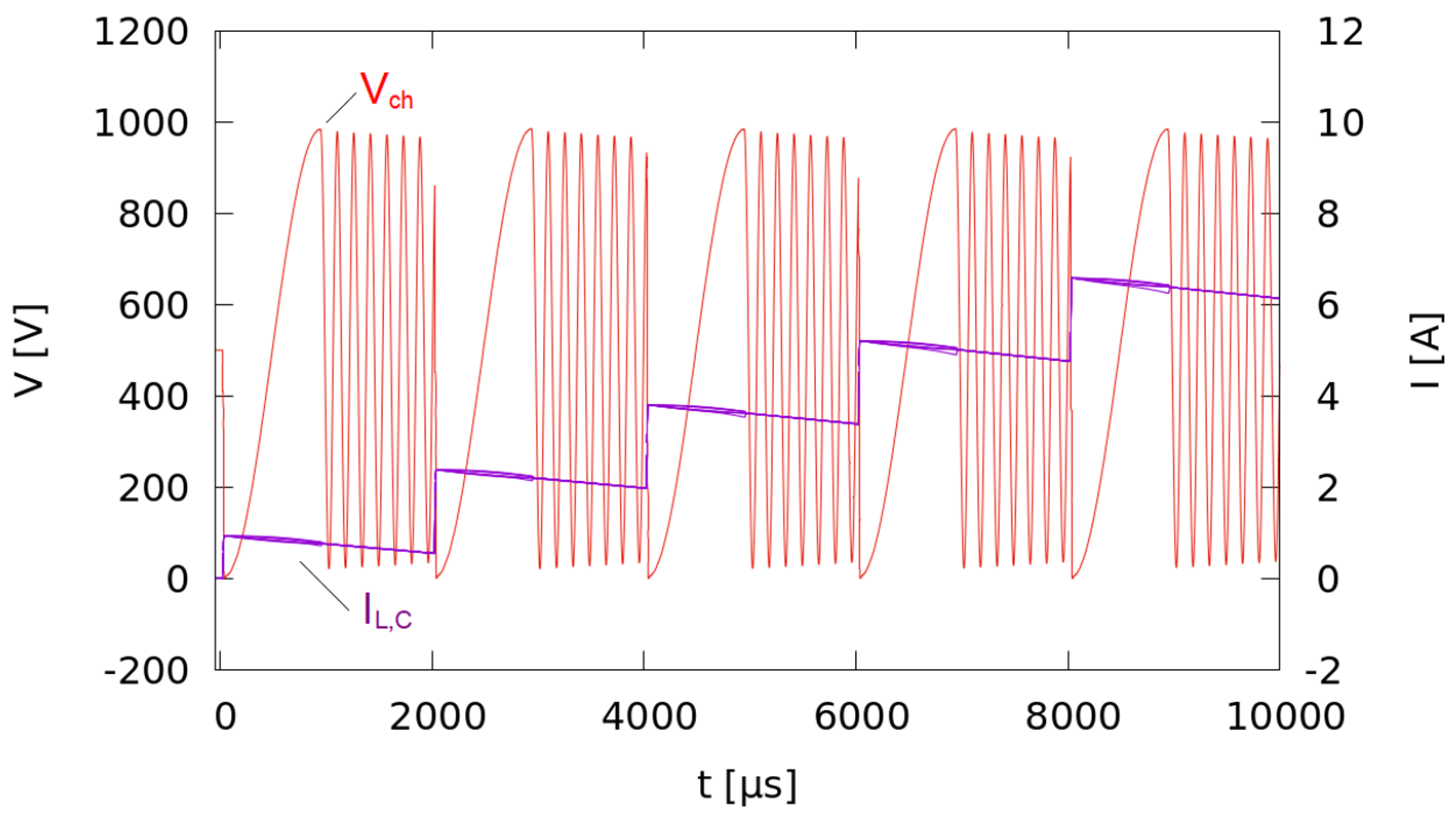
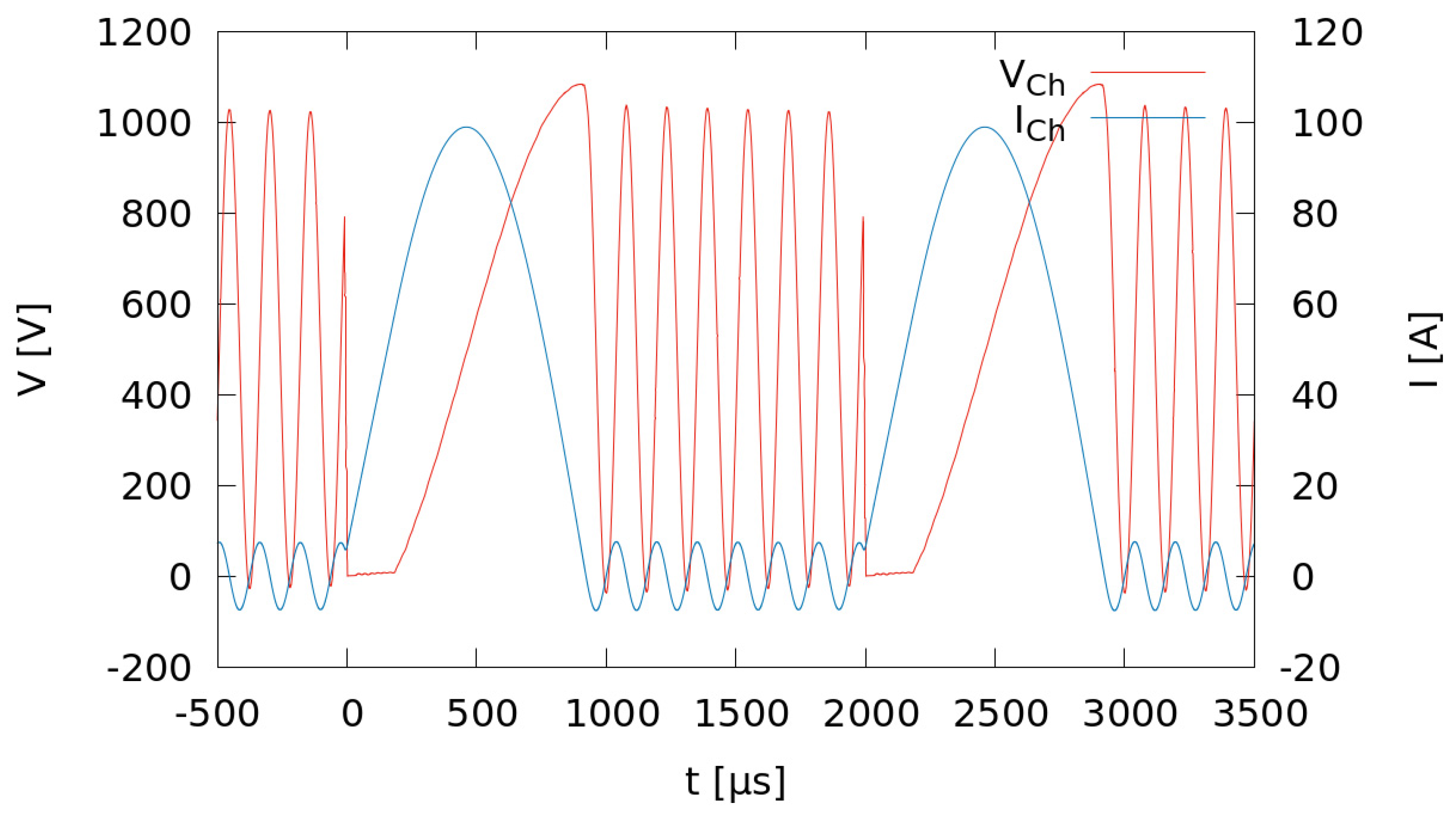
Figure 24 shows the charging current and the charging voltage at the charging input terminal of an 8-stage Marx generator. The on-time of the solid-state switches is 22 µs. The measurement results fit very well with the simulation results shown in 
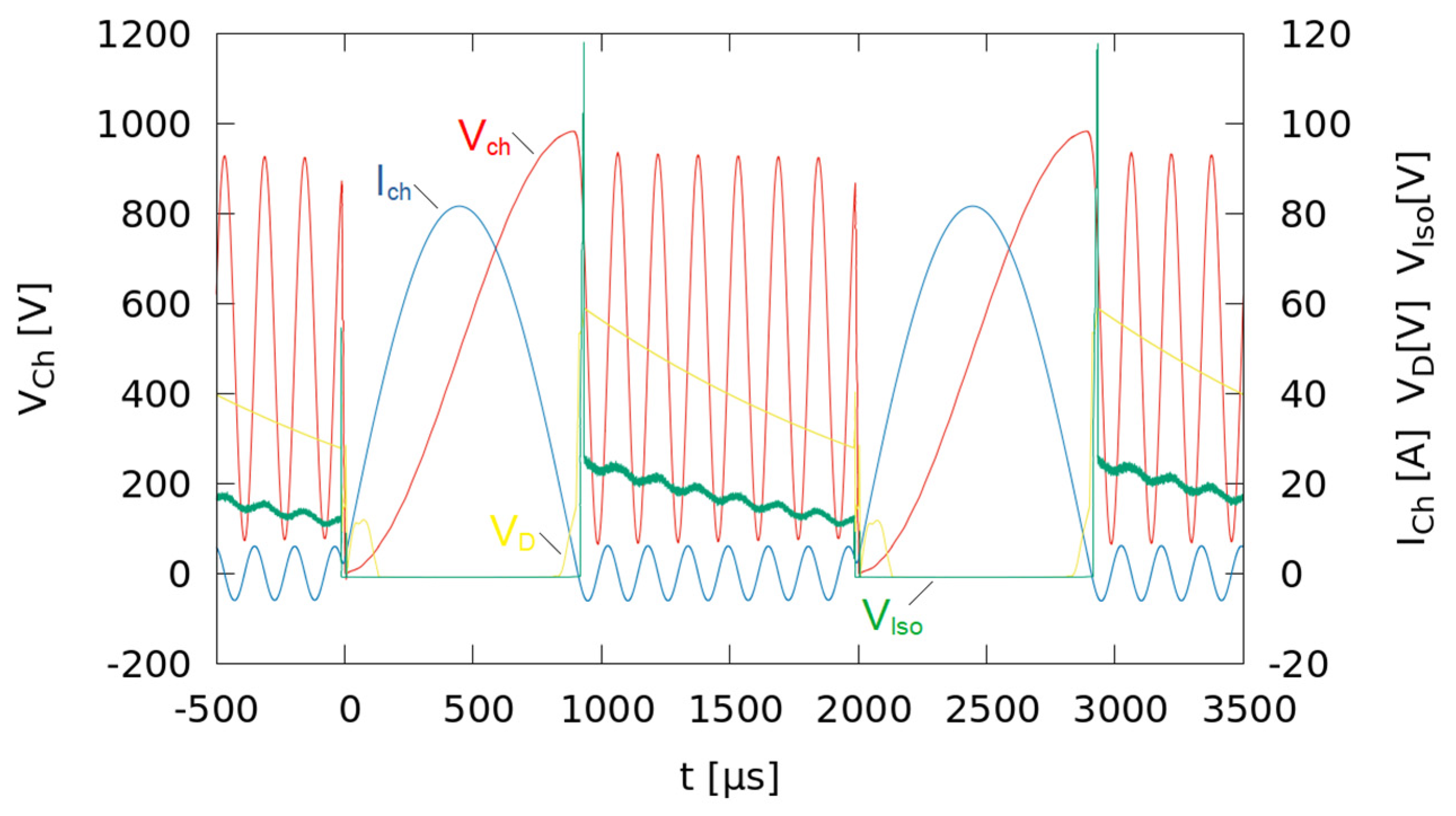
Figure 13 with respect to the charging voltage and charging time and as well as the ringing after charging. Simulation and measurements differ slightly with respect to damping. However, an exact fit of the simulations to measurements was not the goal of the investigations.
Figure 25 shows the measured charging voltage after inserting a diode in series to the charging coil L15. It suppresses the ringing as expected. The measured voltage across the damping resistor RD exhibits a similar shape as the current IRD in Figure 20 and Figure 21 and shows very well the change of the current path of the common-mode current during charging and the finding that damping of the common-mode current occurs mainly after charging of the generator.
For the eight-stage Marx generator, the power dissipation in the damping resistor RD in the order of 50 W is small compared to the average power which the generator delivers to the load. This power is, on average, 12 kW when operating the generator at a charging voltage of 1 kV per stage and 500 Hz pulse repetition rate. However, the total power of the Marx generator and the energy stored in the cores of the current compensated chokes both scales with the number of stages. The energy that is dissipated in the damping resistor RD scales with the number of current-compensated chokes, which is one less than the number of stages. Hence, the ratio of average power dissipated in RD and the total average power of the generator scales with n/(n + 1). For a large number of stages n, the ratio can be approximated as a linear dependency of the number of stages n. Especially for a Marx generator with a larger number of stages, the heat dissipation at the damping resistor needs to be considered. Moreover, with a damping resistor of RD = 20 Ohm, the amplitude of the common-mode current is significantly higher than for the case without a damping resistor. In the presented simulations, the peak value of the common-mode current with RD = 20 Ohm is 3.2 A under steady-state conditions, and without a damping resistor, only 1.8 A. In the latter case, the current through the current-compensated chokes decays to zero right after charging the capacitors. As a consequence, the cores of the current-compensated chokes in the charging path can be designed smaller.
For a design omitting the damping resistor RD, the power supply needs to be designed in such a way that it can cope with a floating potential at its ground-side terminal. This can be accomplished either by static or transient insulation of the power supply versus ground. Static insulation may comprise a transformer as an insulating element. Dynamic insulation may be achieved by adding a second charging coil LRes also to the ground-side current path between the voltage source V1 and the pulse generator and distributing the total inductance equally among both coils. Together with a capacitance between the output terminals of the power supply V1 and ground potential, these inductances form a second-order low-pass filter. Depending on the design, the stray capacitance between the voltage source and ground might be used advantageously for this purpose.
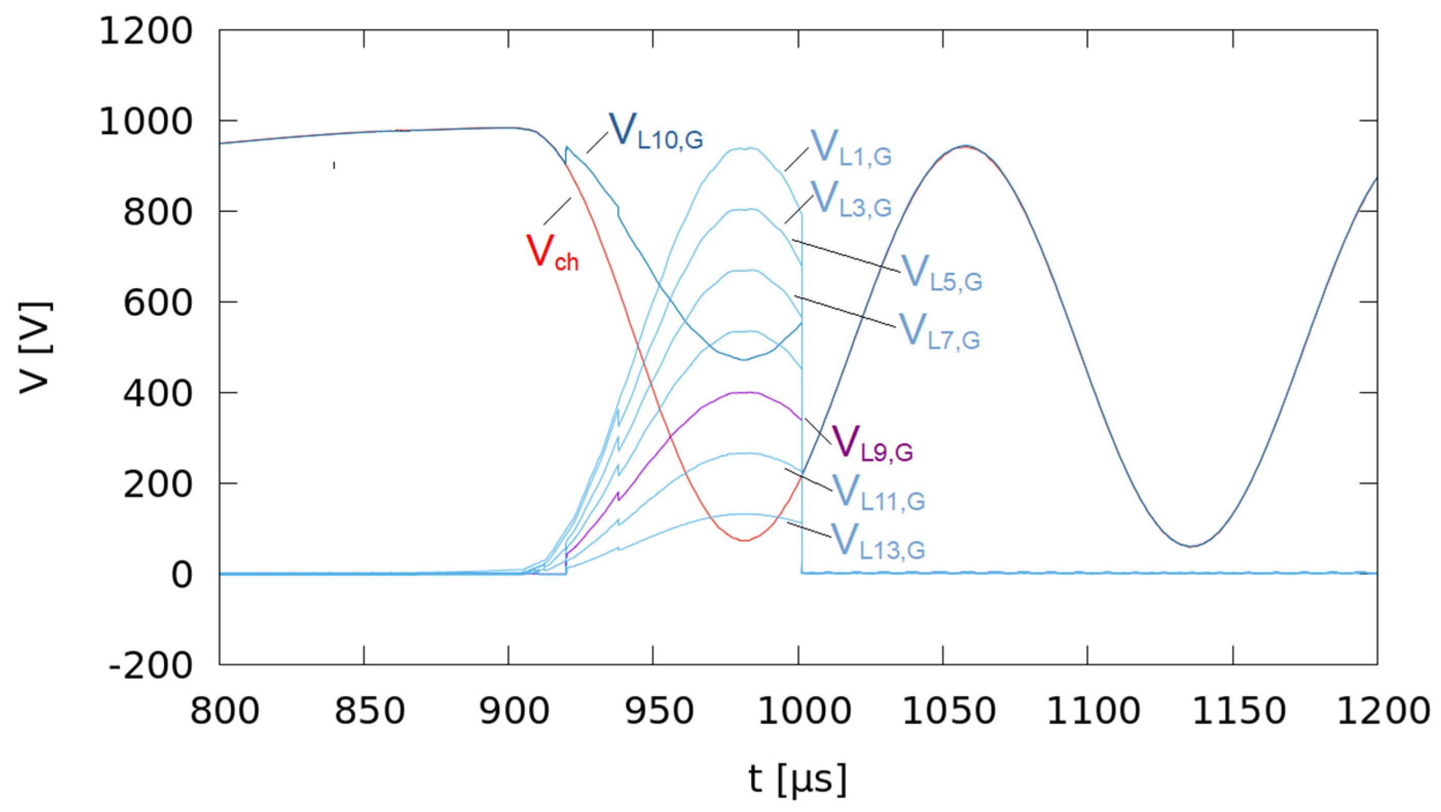
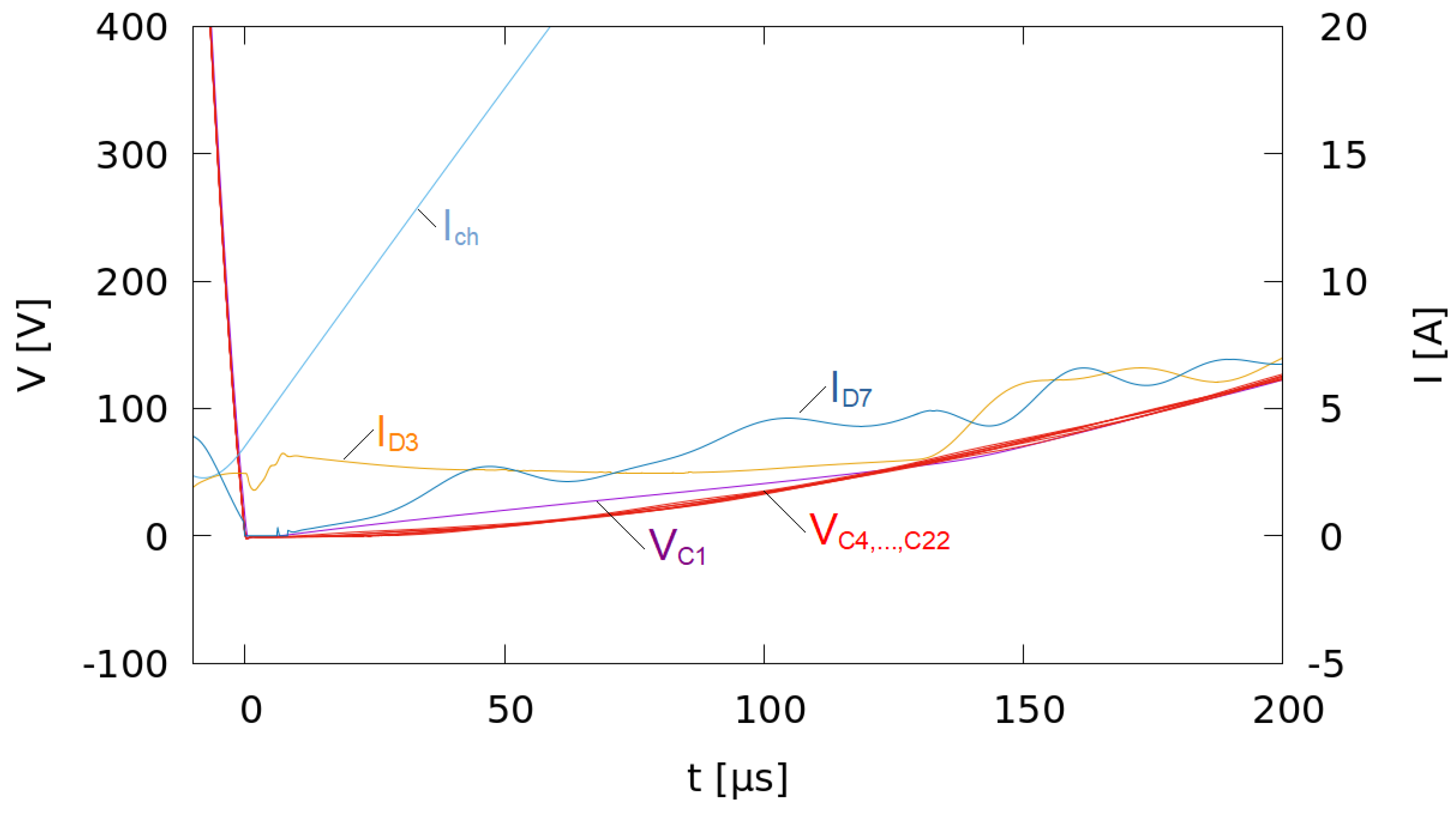
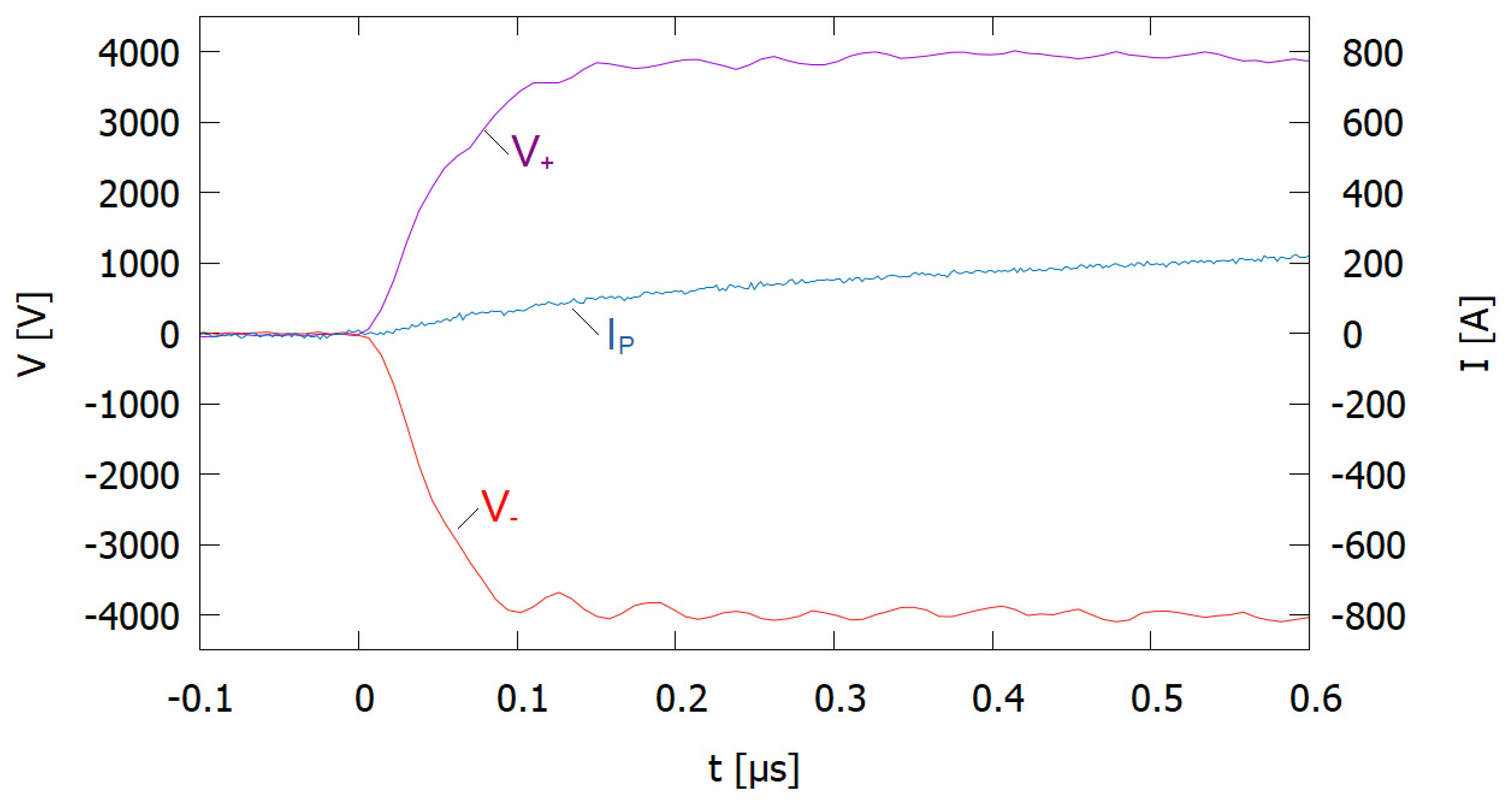
One feature of the presented design is the possibility of energy-efficient soft-switching under almost zero-current conditions both when closing and opening the switches. Figure 26 shows the voltage and current at the positive and negative output terminal of the 8-stage generator. As the voltage rises within less than 100 ns while the current is still low, the switching losses are kept small enough to allow for air-cooling of the semiconductor switches with natural convection in repetitive operation [
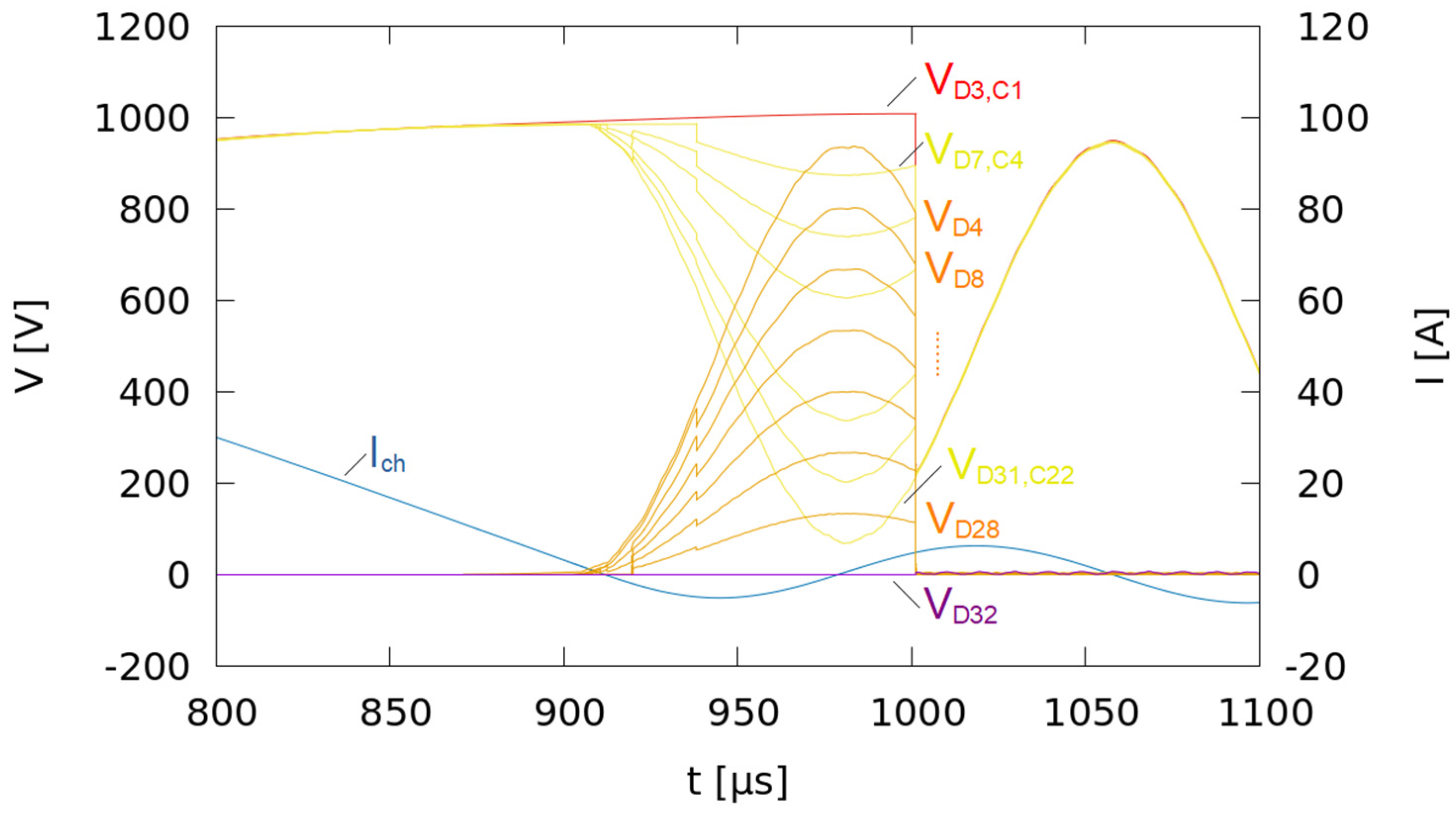
16]. When using the feature of fine-tuning the charging voltage by means of an extended on-time of the switches, the stage switches open under a zero-voltage condition, as the stage capacitors remain uncharged as long as the switches are closed, and the current commutates just after opening the switches to the current path through the stage capacitor. However, when opening the switches before the stage capacitors have been discharged completely, as shown in Figure 16, the switches are opened under hard-switching conditions involving additional switching losses. Therefore, such an operation should be omitted under normal operating conditions.

5. Conclusions

A circuit simulation describing an eight-stage Marx generator with resonant charging in ground-symmetric operation featuring current-compensated chokes as charging coils has been set up in order to study the charging process.
It could be shown that a combination of the resonant charging circuit with a design having only one active switch per stage is capable of fine-tuning the generator’s charging voltage just by modulating the on-time of the switch. This novel feature will be advantageously used for the future setup of such a generator for use in an industrial environment.
Moreover, the simulations revealed that the use of current-compensated chokes in the charging path requires some means for the dissipation of the energy stored in the cores of these chokes due to pulse generation. As a consequence, a damping resistor has been added to the circuit in such a way that it is able to dissipate this energy without actually being part of the current paths for charging or pulse generation.
The results obtained from the simulations have been compared to measurements obtained from an eight-stage Marx generator. They exhibit excellent agreement.
Future work will be devoted to further testing and upscaling of the existing eight-stage Marx generator.

Author Contributions

Conceptualization, M.S. and G.M.; methodology, M.S., J.R. and D.H.; validation, M.S., D.H. and J.R.; investigation, M.S., J.R. and D.H.; writing—original draft preparation, M.S.; writing—review and editing, J.R., D.H. and G.M.; visualization, M.S.; supervision, G.M.; funding acquisition, G.M., M.S. All authors have read and agreed to the published version of the manuscript.

Funding

This research was funded by the technology transfer fund of the Karlsruhe Institute of Technology and the Helmholtz research program MTET.

Institutional Review Board Statement

Not applicable.

Informed Consent Statement

Not applicable.

Data Availability Statement

Not applicable.

Conflicts of Interest

The authors declare no conflict of interest.

References

  1. Vorobiev, E.; Lebovka, E. Electrotechnologies for Extraction from Food Plants and Biomaterials; Springer: New York, NY, USA, 2008; pp. 237–239. [Google Scholar]
  2. Sack, M. Marx-Generator Design and Development for Biomass Electroporation. In Handbook of Electroporation; Miklavcic, D., Ed.; Springer International Publishing: New York, NY, USA, 2016. [Google Scholar]
  3. Marx, E. Verfahren zur Schlagprüfung von Isolatoren und anderen elektrischen Vorrichtungen. German Patent No. 455 933, 12 October 1923. [Google Scholar]
  4. Zabihi, S.; Zare, F.; Ledwich, G.; Ghosh, A. A resonant based Marx generator. In Proceedings of the 2010 20th Australasian Universities Power Engineering Conference, Christchurch, New Zealand, 5–8 December 2010; pp. 1–5. [Google Scholar]
  5. Li, Z.; Wang, X.; Jiang, S.; Wang, Y.; Rao, J. Research on the Bipolar Microsecond Pulse Generator Using the Multistage Resonant Charging. IEEE Trans. Plasma Sci. 2022, 50, 109–115. [Google Scholar] [CrossRef]
  6. Imai, F.; de Novaes, Y.R. Design and Assembly of a Bipolar Marx Generator Based on Full-Bridge Topology Applied to Electroporation. In Proceedings of the 2019 IEEE 15th Brazilian Power Electronics Conference and 5th IEEE Southern Power Electronics Conference (COBEP/SPEC), Santos, Brazil, 1–4 December 2019; pp. 1–6. [Google Scholar] [CrossRef]
  7. Li, Z.; Liu, H.; Jiang, S.; Guo, L.; Rao, J. A High-Current All-Solid-State Pulse Generator Based on Marx Structure. IEEE Trans. Plasma Sci. 2020, 48, 3629–3636. [Google Scholar] [CrossRef]
  8. Elgenedy, M.A.; Massoud, A.M.; Ahmed, S.; Williams, B.W.; McDonald, J.R. A Modular Multilevel Voltage-Boosting Marx Pulse-Waveform Generator for Electroporation Applications. IEEE Trans. Power Electron. 2019, 34, 10575–10589. [Google Scholar] [CrossRef] [Green Version]
  9. Bluhm, H. Pulsed Power Systems—Principles and Applications; Springer: Berlin/Heidelberg, Germany, 2006. [Google Scholar]
  10. Sack, M.; Ruf, J.; Herzog, D.; Müller, G. Erdungskonzept für einen halbleitergeschalteten Marxgenerator mit resonanter Aufladung. In Proceedings EMV Kongress 2022; Garbe, H., Ed.; Apprimus: Aachen, Germany, 2022; pp. 397–404. [Google Scholar]
  11. Analog Devices: LTspice. Available online: https://www.analog.com/en/design-center/design-tools-and-calculators/ltspice-simulator.html (accessed on 20 July 2022).
  12. Sack, M.; Ruf, J.; Herzog, D.; Müller, G. Auxiliary Power Supply for a Semiconductor-based Marx Generator. In Proceedings of the 2021 International Aegean Conference on Electrical Machines and Power Electronics (ACEMP) & 2021 International Conference on Optimization of Electrical and Electronic Equipment (OPTIM), Brasov, Romania, 2–3 September 2021; pp. 220–224. [Google Scholar] [CrossRef]
  13. Sack, M.; Herzog, D.; Ruf, J.; Müller, G. Resonant Charging Circuit for a Semiconductor-based Marx Generator for an Electroporation Device. In Proceedings of the IEEE International Power Modulator and High-Voltage Conference, Knoxville, TN, USA, 19–23 June 2022. [Google Scholar]
  14. Sack, M.; Attmann, F.; Müller, G. EMV-Aspekte beim Entwurf einer Elektroporationsanlage. In Proceedings EMV Kongress 2010; Garbe, H., Ed.; Mesago, Messe Frankfurt GmbH: Düsseldorf, Germany, 2010; pp. 635–642. [Google Scholar]
  15. Hameg. Programmable LCR-Bridge HM8118, User Manual; Hameg Instruments: Mainhausen, Germany, 2012. [Google Scholar]
  16. Sack, M.; Herzog, D.; Müller, G. Abschlussbericht zum Projekt PEF4CHIPS (Final Report about the Project PEF4CHIPS); Karlsruhe Institute of Technology: Karlsruhe, Germany, September 2022. [Google Scholar]
Figure 1. Simulated pulse voltage VP and pulse current IP at the output terminal of an 8-stage Marx generator with free-wheeling diodes. After the discharge of the stage capacitors, the pulse current commutates to the free-wheeling diodes (ID).
Applsci 12 12481 g001
Figure 2. Simplified circuit for basic studies on resonant charging.
Applsci 12 12481 g002
Figure 3. Circuit simulation model for an 8-stage Marx generator with resonant charging.
Applsci 12 12481 g003
Figure 4. Simulated voltages at nodes in the positive charging path of the current-compensated chokes versus ground (VL1,G, VL3,G … VL13,G), and the voltage of the ground-side connection of the power supply (VL10,G). Thereby, the nodes are named according to the respective coil of the current-compensated choke on the right-hand side seen from the node. VCh marks the simulated charging voltage at the input terminal for charging the Marx generator according to the schematic in Figure 3. (RD: open circuit).
Applsci 12 12481 g004
Figure 5. Simulated voltages across the stage capacitors C1, C4, C7, C10, C13, C16, C19, and C22 according to Figure 3, together with the generator’s charging current Ich (RD: open circuit).
Applsci 12 12481 g005
Figure 6. Simulated voltages at the charging path referenced to the negative poles of the stage capacitors for the 8-stage Marx generator according to Figure 3. The voltages at each stage across the series connection of the diode between the positive charging path and stage and the stage capacitor are marked as VD3,C1 for the leftmost stage and VD7,C4 … VD31,C22 for the other stages in the order from left to right. The voltages across the diodes to the negative charging path are named according to the respective diodes (VD4, VD8 … VD32). The curve named ICh shows the charging current at the generator’s charging input.
Applsci 12 12481 g006
Figure 7. Energy stored in the core of two current-compensated chokes (WCore) and common-mode current ICM through the chokes (Simulation for current-compensated chokes comprising L1, L2 and L3, L4 according to Figure 3, RD: open circuit, ton = 22 µs).
Applsci 12 12481 g007
Figure 8. Simulated common-mode currents in the charging path (IL,C) for the first five pulses with RD almost 0 Ohm. Thereby, IL,C is the superposition of the almost equal common-mode currents in all current-compensated chokes. VCh is the charging voltage at the input terminal for charging the Marx generator.
Applsci 12 12481 g008
Figure 9. Simulated voltages across the stage capacitors C1, C4, C7, C10, C13, C16, C19, and C22 according to Figure 3, together with the generator’s charging current Ich (RD = 20 Ohm).
Applsci 12 12481 g009
Figure 10. Simulated charging voltage Vch and the charging current Ich at the charging input terminal of the 8-stage Marx generator according to Figure 3, voltage VD across the damping resistor RD (i.e., R3 according to Figure 3), voltage VISO of the ground-side terminal of the power supply versus ground (i.e., VL9,G according to Figure 4), on-time of the solid-state switches: 22 µs.
Applsci 12 12481 g010
Figure 11. Losses at the damping resistor RD (R3 in Figure 3): Power PRD and current through RD (IRD).
Applsci 12 12481 g011
Figure 12. Energy stored in the cores of two current-compensated chokes (WCore) and common-mode current IC through the chokes (Simulation for current-compensated chokes comprising L1, L2 and L3, L4 according to Figure 3, RD = 20 Ohm, on-time of the solid-state switches: ton = 22 µs).
Applsci 12 12481 g012
Figure 13. Charging voltage Vch and the charging current Ich at the charging input terminal of the generator, on-time of the solid-state switches: ton = 22 µs.
Applsci 12 12481 g013
Figure 14. Charging voltage Vch and the charging current Ich at the charging input terminal of the generator, on-time of the solid-state switches: ton = 200 µs.
Applsci 12 12481 g014
Figure 15. Energy stored in the cores of two current-compensated chokes (WCore) and common-mode current IC through the chokes (Simulation for current-compensated chokes comprising L1, L2 and L3, L4 according to Figure 3, RD = 20 Ohm, on-time of the solid-state switches: ton = 200 µs).
Applsci 12 12481 g015
Figure 16. Simulated voltages across the stage capacitors C1, C4, C7, C10, C13, C16, C19, and C22 according to Figure 3 together with the generator’s charging current Ich (RD = 20 Ohm, on-time of the solid-state switches: ton = 200 µs).
Applsci 12 12481 g016
Figure 17. Charging voltage Vch and the charging current Ich at the charging input terminal of the generator, on-time of the solid-state switches: ton = 10 µs.
Applsci 12 12481 g017
Figure 18. Distribution of the charging current along the charging path according to the position in the generator for an on-time of the solid-state switches of 22 µs. The charging currents ILl,D through the coils of the left four current-compensated chokes are shown in light-blue colour, and the charging currents ILr,D through the coils of the right three current-compensated chokes in violet colour. Thereby, the current decays stepwise from the centre towards both ends of the generator. Vch and Ich denote the charging voltage and the charging current at the generator’s input terminal, respectively.
Applsci 12 12481 g018
Figure 19. Distribution of the charging current along the charging path according to the position in the generator for an on-time of the solid-state switches of 200 µs. The notation is equal to Figure 18.
Applsci 12 12481 g019
Figure 20. Common mode component of the currents in the current-compensated chokes IL,C in violet colour except for the common mode current component in the leftmost current-compensated choke IL1L2,C, which is shown in blue colour. Vch and IRd denote the charging voltage at the generator’s input terminal and the current through the damping resistor RD (R3, according to Figure 3), respectively.
Applsci 12 12481 g020
Figure 21. Common-mode current components through the diodes are shown in light-blue colour.
Applsci 12 12481 g021
Figure 22. Voltages across the capacitors C1 (VC1) and C4, C7, C10, C13, C16, C19, and C22 (VC4,…,C22), currents through D3 (ID3) and D7 (ID7) according to Figure 3 together with the generator’s charging current Ich (RD = 20 Ohm, on-time of the solid-state switches: ton = 22 µs).
Applsci 12 12481 g022
Figure 23. Equivalent circuit showing current paths.
Applsci 12 12481 g023
Figure 24. Measured charging voltage and the charging current at the charging input terminal of an 8-stage Marx generator, on-time of the solid-state switches: 22 µs [10].
Applsci 12 12481 g024
Figure 25. Measured charging voltage Vch and the charging current Ich at the charging input terminal of an 8-stage Marx generator with a diode in series to LRes, voltage VD across the damping resistor RD, on-time of the solid-state switches: 22 µs [10].
Applsci 12 12481 g025
Figure 26. Measured rise of the pulse voltage at the positive (V+) and negative (V) output terminal of an 8-stage Marx generator in ground-symmetric operation and the pulse current IP [16].
Applsci 12 12481 g026
Publisher’s Note: MDPI stays neutral with regard to jurisdictional claims in published maps and institutional affiliations.

