Article

Late-Stage Optimization of Modern ILP Processor Cores via FPGA Simulation

School of Computer, National University of Defense Technology, Changsha 410005, China
*
Authors to whom correspondence should be addressed.
Appl. Sci. 2022, 12(23), 12225; https://doi.org/10.3390/app122312225
Submission received: 1 September 2022 / Revised: 23 November 2022 / Accepted: 23 November 2022 / Published: 29 November 2022

Abstract

:
Late-stage (post-RTL implementation) optimization is important in achieving target performance for realistic processor design. However, several challenges remain for modern out-of-order ILP (instruction-level-parallelism) processors, such as simulation speed, flexibility, and complexity problems. This paper restudy FPGA simulation as an effective performance simulation method and proposes FPGA-enhanced design flow as an effective method to address these problems. It features a late-stage aware RTL design that parameterizes various potential design options induced from early-stage optimization. This flow enables the feasibility of late-stage design space exploration. To resolve the performance accuracy of the FPGA system for peripheral designs, reference models are introduced. With an example implementation of out-of-order core running up to 80 MHz, the experimental results show that the proposed method is practical and allows the fine-grain optimization of the processor core to be more effective.

1. Introduction

The microarchitecture design of a processor generally comprises two stages. Early-stage optimization is performed before RTL (register transfer level) implementation, which defines the microarchitecture specification. Late-stage optimization is performed after the initial RTL implementation, which aims for satisfactory design in terms of performance and other metrics. The demand of recent optimization methods for enhanced efficiency requires increasingly fast and accurate simulation across the entire system stack as the modern out-of-order ILP (instruction-level-parallelism) processor core design becomes more complicated. This demand makes late-stage optimization increasingly important because of its advantages, such as accuracy. Moreover, the increasing need to optimize the existing processor core RTL with moderate effort for other applications or focus on single-thread performance remains important [1,2].
Designing effective simulators for late-stage performance simulation is challenging due to its strict requirement in accuracy, speed, and full system capability [3]. Table 1 provides six cycle-accurate simulation methods in two design stages for modern processor cores and lists rough comparison results obtained from our prior design experience. A few key metrics, such as speed, accuracy, configurability, design effort, and cost for designing the performance simulator were considered. The speed is measured by the simulation frequency for the target processor. The accuracy is how the simulation performance results close to the target processor. The configurability aims to provide designers different processor design options to explore. The design effort is the design complexity and workload of designing the simulator. The cost is the price for implementing the simulator.
RTL simulation models the processor core at a low abstraction level by incorporating full function and latch-accurate pipeline flow timing. This process slows the speed of the RTL software simulator and is thus rarely used in actual microarchitecture optimization. A cycle-accurate software simulator, such as SimpleScalar [4] or GEM5 [5], can also be used for late-stage optimization. However, software simulators are typically inaccurate and operate with abstract, incomplete, or missing components. A cycle-accurate simulator can be implemented similarly as RTL, but doing so requires additional work, such as in RTL implementation, and reduces speed.
The FPGA simulator [6,7,8,9,10,11,12,13,14,15] is an appealing means of late-stage optimization due to its advantages, such as speed and low cost. The FPGA system is already mature for simple in-order processors. Achieving target speed [16] is difficult for modern complex out-of-order processors due to issues in capacity and structural complexity. A previous study [17] indicated a speed problem, whereas others highlighted such issues as extended setup process, which results in high simulation turnaround time; significant effort to design the change in RTL for each experimental machine, and accuracy for simulated peripheral designs. FPGA technology has significantly improved recently, and we show that it can be used as a method for the practical performance simulation of the late-stage optimization of modern out-of-order cores. Furthermore, we introduce reference models to solve the accuracy problem of peripheral designs on FPGA system.
To demonstrate, we use a typical out-of-order core to develop a corresponding FPGA simulation system for late-stage optimization. It implements a complete computation platform equipped with a modern complex processor core into a single FPGA chip. It can achieve up to 80 MHz processor frequency. An efficient microarchitecture exploration flow can be formed, and FPGA simulation is used as a new performance test iteration for rapid optimization flow at the late stage. For the processor core, coarse-grain optimization can be done at the early stage using software simulation, whereas fine-grain optimization can be performed at the late stage using FPGA simulation. It features a late-stage aware RTL design, which parameterizes various late-stage design options derived from early-stage optimization. This flow minimizes the RTL change effort for late-stage optimization. Using widely used SPEC CPU benchmarks as an example, we show the effectiveness of FPGA simulation for late-stage optimization.
The rest of the paper is organized as follows. Section 2 summaries the FPGA-enhanced design methodology. Section 3 introduces the FPGA implementation. Section 4 provides the evaluation results and case studies. Section 5 describes the related works, and Section 6 concludes this paper.
In contrast to previous works, we believe this paper makes the following unique contributions:
(1) We identify the potential benefits of late-stage optimization, which is rarely studied, and use the proposed FPGA-enhanced design flow to accomplish it for fine-grain microarchitecture optimization.
(2) We introduce an FPGA system for demonstration, which ports a modern processor core with extensive optimizations at 80 MHz frequency. The reference model is also proposed to resolve the performance accuracy of the FPGA system for peripheral designs.
(3) Several interesting results are found through case studies: firstly, using reduced input data set could produce inaccurate performance evaluation results, compared with the real input data set; secondly, FPGA-aware design space exploration could be very useful, i.e., small configuration change results in noticeable performance variation.

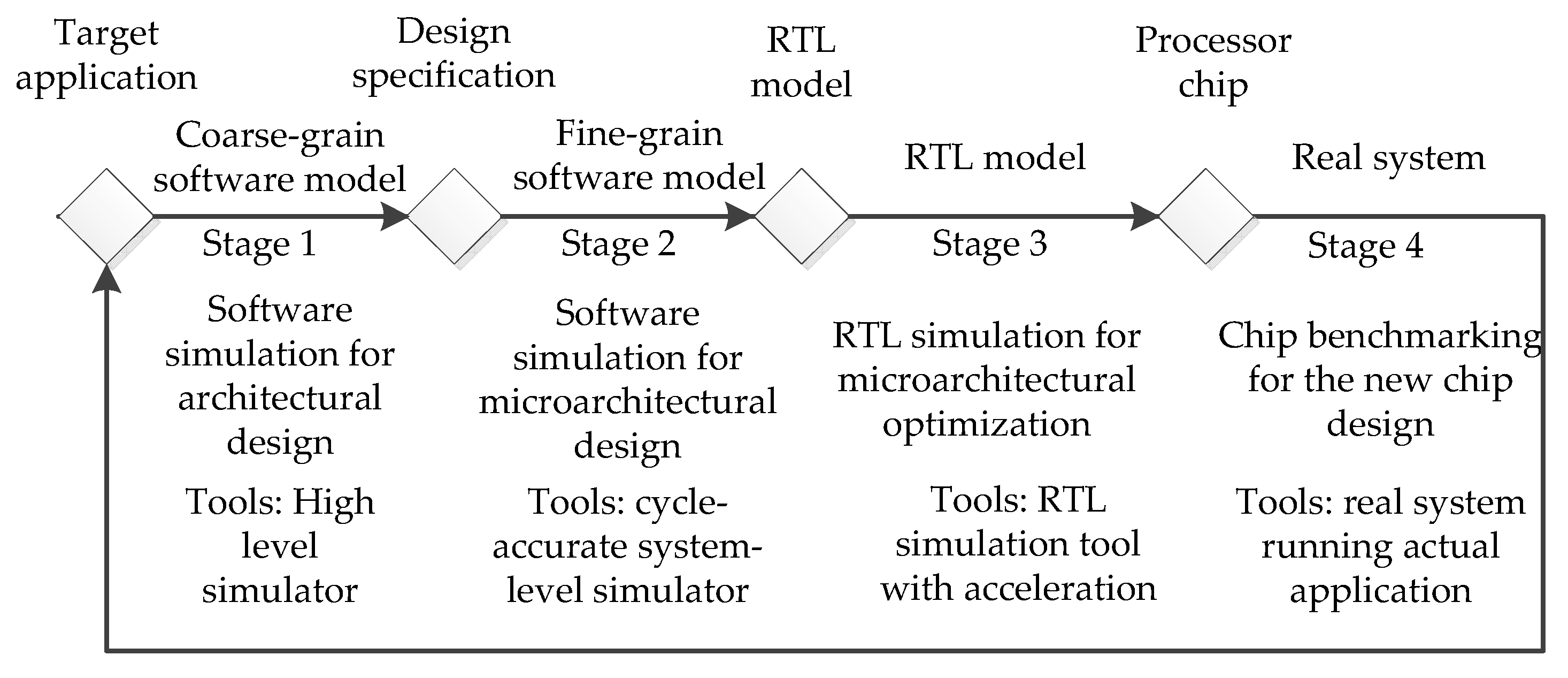
2. Conventional Processor Design Flow

Figure 1 illustrates conventional processor design flow for architecture optimization based on simulation. It can be conceptually identified as following four stages: (1) Given the target applications or representative benchmarks, a high-level simulator is used to explore the architectural design space. It determines the potential designs space by using rough estimates of performance, power, chip area and pin count, etc. (2) Architectural simulations which define the microarchitecture or the internal organization of the processor, for example, the number of arithmetic-logical units (ALUs), the size of the caches, the number of processor pipelining stages, the structure of branch predictor, etc. (3) Register transfer level (RTL) simulations which model the processor core at a lower abstraction level. It incorporates full function as well as bit-accurate timing. For simulation acceleration, the commercial emulator and FPGA prototyping are often used. (4) If test chips are available, then chip benchmarking can be done with performance monitor unit (PMU). This evaluation results can be used to direct the next round processor design.
These four main steps require different benchmarking simulations. The key optimization steps for processor core design are Stage 2 (early-stage) and Stage 3 (late-stage). Though the results at Stage 4 using chip benchmarking in the form of test chip or previous generation chip would be adequately fast and accurate, this method is design non-reconfigurable and cost unbearable. Furthermore, it cannot obtain all the required information for analysis. Most simulation-based architectural optimizations focus at Stage 2 using softwarebased simulators. This is because they are easily to implement and usually flexible through parameterizations, allowing a large variety of experiments to be performed. There are also some FPGA simulators to do early-stage optimization with simplified or abstract models, for example, FAME simulators at level 001 to 111 [17], Fabscalar [18]. For stage 3, the initial RTL implementation can be optimized through RTL simulation. The software-based simulation can also be used for such purpose. These simulation methods are relatively slow. Though one can use the truncated applications, sampled benchmarks or reduced input data set to reduce the simulation time, these methods would also possibly lose simulation accuracy and leave the performance results in doubt. This leads to a fact that only after tapeout of the processor design, we can get its accurate performance results.

3. FPGA-Enhanced Design Flow

Figure 2 illustrates the FPGA-enhanced design flow for processor cores. This methodology divides the optimization tasks into two categories of optimization: coarse- and fine-grain. Coarse-grain optimization can be done at the early stage, whose simulations mainly run on an adequate cycle-accurate software simulator. Meanwhile, fine-grain optimization can be done at the late stage, whose simulations run on a fast FPGA system. It features a late-stage aware RTL design. Coarse-grain optimization is similar to the conventional optimization flow. The main difference between them lies in the output of the coarse-grain optimization step, which is aware of late-stage optimization. It is no longer merely an RTL model with a single configuration but a set of parameterized models for varying potential design options. Although late-stage optimization achieves high accuracy at the expense of flexible design options, it is adequate for constrained optimization at the late stage. The potential options can be derived from three sources: (1) Options that cannot be evaluated precisely in the coarse-grain optimization step. The simulator may not precisely realize all system features or use simplified applications for evaluation due to limitations in implementation. If a design option evaluation requires accurate simulation, then late-stage optimization is needed. (2) Options that have performance differential below a threshold. (3) Options that can be easily implemented through RTL parameterization.

3.1. Categorization Decision Method for Early- and Late-Stage

There are several general categorization rules, which will be beneficial for improving the effectiveness of microarchitecture optimization. Based on the experimental results and experiences in this study, Figure 3 presents the detailed categorization decision method of potential design options in different stages. Five factors are considered for categorization, as listed in Table 1. The potential design options go through these selection procedures to find their appropriate simulation stages.
The first selection factor is design effort, which is crucial for late-stage optimization. It is recommended that if a design option can be easily changed in RTL implementation, then late-stage optimization is preferred. After this selection procedure, design options with medium efforts are entered to the next accuracy selection procedure. Three cases with high accuracy requirement could be late-stage options: (1) large performance differences among different applications; (2) large performance impact with fine-grain optimization; (3) small performance variation, whose performance improvement may be less than simulation error. We can introduce a threshold to define such options. This is an interesting situation, where their accuracy requirement may be known only after early-stage simulation. Hence, the categorization may go through the process more than one time before and during early-stage optimization. So several design options may be explored in both early- and late-stage simulation. Fortunately, many these options belong to the late-stage options in the first selection procedure. As we already know that they can be explored in late-stage simulation, their early-stage simulations are not needed. For the performance selection procedure, late-stage optimization is preferred. However, if reduced accuracy is acceptable, early-stage optimization can be a choice. For the configurability selection procedure, it is related to the design effort. Unlike early-stage options, late-stage options are limited to the implementation feasibility. For example, the buffer size cannot increase infinitely. For the cost selection procedure, we should consider what resources we have, such as server cluster, FPGA boards and so on, then calculate the rough simulation time and associated design time to make the best trade-off for performance optimization.

3.2. Late-Stage Aware RTL Design

To understand the design options suitable for the late stage, Table 2 shows an example. It lists the design options specified by a common configuration file from the GEM5 simulator (configs/common/configuration.py) [5]. The parameter column in the table lists their configuration names in GEM5. The op-type column lists their optimization types, which are classified into three categories: VT, which can be easily parameterized; PT, each value of which represents a design policy; and CT, which denotes whether or not to choose a design feature. Although certain PT parameters, such as Count and fetchWidth, are numbers, they cannot be regarded as VT because their values affect many other modules. For example, the fetchWidth parameter considerably affects the design of the instruction cache, branch predictor, and front-end pipeline. The RTL column lists their RTL configuration methods for the design options, which are described in Section 3.2. The effort column provides a coarse-grain classification for RTL design effort ratings. Design options with “E” and “H” are preferred for late- and early-stage optimization, respectively. Options with “M” are determined by the actual design target. For example, if the hit_latency parameter in the L2 cache can be implemented with a minimal value in the late-stage simulator, it can be classified as a late-stage option. If the TableSize parameter in the BPU has large performance differences among various applications at the early stage, it also can be classified as a late-stage option. Overall, if we find that design options are explored in excess at the late stage, a trade-off between design and simulation time should be made. Thus, several design options that were originally considered to be late-stage likely become early-stage.

3.3. RTL Design Categories

The key to utilizing late-stage optimization is that the design effort for RTL change should be affordable. The late-stage aware RTL design can help minimize RTL change effort. Table 2 shows that the late-stage aware RTL design options are divided into four categories: (1) PAR, whose RTL change can be conducted by a parameter identifier. Once the parameterized design is determined before RTL implementation, PAR is the easiest case for RTL change and most suitable for late-stage optimization. (2) MIN, whose implementation difficulty is determined by the design of its minimal value. This option typically denotes the latency of an operation, such as the issueLat and opLat parameters in FUs. We can introduce a configurable delay unit to implement other lengthy latencies on the basis of a minimalist design. The difficulty of minimizing latency in late-stage optimization can be reduced in two ways: increasing the cycle time if the performance reduction is bearable and not implementing several minimal values. For options whose latency affects several modules, configuration becomes increasingly difficult. Hence, exploring such a design option at the early stage is recommended. For example, the various latencies parameter of the pipeline belongs to this type. (3) MAX, whose difficulty in implementation is determined by the design of its maximum value. This option typically refers to the buffer size or operation width. Similar to the MIN option, MAX allows an increase in cycle time or omission of other options to handle such a difficulty. For small sizes or widths, parameter primitives or mask signals can be introduced on the basis of the design with the maximum value. (4) IMP, which requires a nearly new RTL design for late-stage optimization. This option may add to the design effort burden of RTL implementation. Therefore, our principle is that an option can be implemented only if it can be used in one type of processor core. Otherwise, only early-stage optimization should be considered. Nevertheless, certain cases call for the design of various processor cores, thereby rendering these IMP options with different values useful.
Using the late-stage aware RTL design method, we can see that most of the design parameters can be optimized at the late stage with minimal design effort. Only a few design parameters cannot be optimized at this stage. This contrast provides a considerable opportunity for architects to apply FPGA simulation.

4. FPGA Implementation

4.1. PNX Processor Architecture

To demonstrate the effectiveness of the proposed methodology, we introduce a concrete example, which is based on an our in-house PNX processor. The baseline PNX processor is a typical modern four-issue processor with out-of-order execution, which has 10+ pipeline stages and supports a 128-bit SIMD execution. It has separate L1 instruction (ICache) and L1 data (DCache) cache and a shared L2 cache. The data can be prefetched in a stride-detecting manner for the L1 DCache and the unified L2 cache. A wide range of parameters must be tuned to explore the best trade-offs in terms of the selected system merits, such as performance and area, and consequently optimize performance.
Several late-stage performance simulations require various RTL models for numerous design options. The configurability of the PNX processor is largely determined by the result of the late-stage aware RTL design. Each processor model corresponds to a fixed microarchitecture for performance evaluation and optimization. Table 3 lists examples of the configuration. Brackets are used to denote the basic processor configuration. These options are composed of “E” and “M” design efforts. For other design options with “E” and “M,” modifying the processor model is also feasible. The design options are notably beyond the range of the basic options with the MAX or MIN type and unsuitable for late-stage simulation. For example, assume decodeWidth is 4. If we model a processor with decodeWidth larger than 4, then its design effort should be “H”.

4.2. FPGA System

Figure 4 shows a conceptual block diagram of the FPGA system. The system comprises two parts: FPGA hardware and management software. The FPGA hardware hosts the target processor core and other components that facilitate performance analysis. The processor core has a conventional PMU that can perform general performance analysis. For information that cannot be obtained from the PMU, a specially designed PMU (SD-PMU) outside the processor core can be utilized. The SD-PMU is capable of supporting any processor hardware analysis because it can connect to any hardware signal in the processor if required. Another FPGA hardware component, the config/reset unit (CRU), is used to control the configuration of a design under test (DUT), such as frequency regulation and system reset.
Figure 5 shows the logic view of FPGA implementation of PNX processor. This is also a minimal computing system that facilitate the performance evaluation and optimization. We have omitted some ASIC components that do not necessarily required in the FPGA simulation, such as USB controller. It contains a single PNX processor core with other peripherals connected through on-chip bus. The pipeline structure of PNX processor is shown in Figure 6.
Management software contains the test manager and result analyzer, which run the host computer for FPGA environment management. The test manager is used to manage the generated FPGA bit files, control the FPGA configurations for several design options, and provide the reset signals for the FPGA system. The result analyzer collects and reports performance data from SD-PMU and PMU. Synplify Pro is used for high-level synthesis, and the Xilinx Vivado design suite is used for placement and routing onto the FPGA device. The system software, which runs on the target processor, consists of the BIOS program, operating system, and related test benchmarks.
The FPGA hardware is generally flexible, and most development boards with adequate ASIC gate capacity can be used in FPGA simulation. The hardware comprises one main FPGA board and related peripherals. The main board contains a large FPGA chip, namely, an XCVU440. The main board should also have DDR SO-DIMM on-board sockets, which support large memory. A host computer interacts with the main FPGA boards using a standard ethernet or USB interface. All control functions, such as downloading an FPGA configuration, programming clock generation, self-testing, and running the DUT, are exposed to the users. The peripherals can be designed as daughter boards to the main FPGA boards, which are designed to be reusable to reduce cost. The current configuration has four external boards: a low-speed storage board, which contains a flash and an SD card; a physical (PHY) unit board, which provides ethernet connection with the host machine; an SRAM module board, which expands memory for FPGA implementation; and a GPIO extension board, which contains pin headers, LEDs, push buttons, and a JTAG interface.

4.2.1. Performance Optimization

To efficiently implement the PNX core on the FPGA chip, methods other than general FPGA mapping techniques should be applied. The PNX processor has many highly ported memory structures, such as associative arrays or content addressable memory, which are expensive to implement on FPGA. We use the recently proposed live value table design method [19], which significantly improves operating frequency. Meanwhile, the clock gating issue is directly disabled by FPGA implementation. This cancellation is done by defining the macro that can remove the clock gating in the FPGA code, which is fairly simple. However, if the clock gating is functional, we should convert them using the EDA tool or eliminate them through manual modification.
Achieving timing closure for large and complex FPGA designs at high speeds is a big challenge. In the proposed FPGA platform, RTL modifications without accuracy loss are conducted to improve performance; such modifications include critical path segmentation and register balancing. If the FPGA implementation does not initially achieve timing closure, iterative optimizations are used [20]. Furthermore, the hierarchical design flow [21] enables module analysis and reuse independent of the rest of the design. This advantage can benefit performance optimization, especially for critical modules.

4.2.2. Simulation Accuracy

To preserve the accuracy of performance evaluation on the FPGA system, functional and timing behaviors of hardware structures on FPGA are designed to be identical to its ASIC implementation. This process is easily conducted for the internal processor logic but a non-trivial task for peripheral designs on FPGA. For the target performance model, peripheral designs should adjust their design proportional to the processor core and consider frequency and timing behaviors. A major challenge comes from the absolute speeds involved in the DDR memory [22]. The processor core in FPGA is relatively slower than the DDR memory, which is not the case in reality. To solve this problem, we propose using a virtual DDR model as a reference model. Unlike the conventional memory system, it contains two additional components: DDR access control unit and virtual DDR model with no memory. The timing behavior of the virtual DDR model precisely conforms to the target system. We can use its timing to control the FPGA memory access because it is slower than the FPGA DDR memory. For simplicity, we use a real DDR to provide a large memory and use the virtual DDR model to provide precise timing.

4.2.3. Design Space Exploration

For design space exploration, implementing various design options should be easy and fast. Through the late-stage aware RTL design, the design options in FPGA can be configured via script. It will automate the process of changing the design options by modifying parameters or RTL files. Then, synthesis and implementation can be performed automatically to generate an FPGA bit file. Most design options can share the same FPGA constraint files through a hierarchical design. However, a few cases for changing a constraint file because of imprecise constrained design remain. If such a case happens, manual intervention should be conducted in the implementation process. Alternatively, such a process can be done on a server cluster and simultaneously run test benchmarks on FPGA.

5. Evaluation

5.1. FPGA Implementation Results

Table 4 lists the results of FPGA implementation for the basic PNX processor. Section 4.1 discusses its parameters, which are specified in Table 3. The memory structures for the basic processor are implemented inside the FPGA. For other configurations that require additional RAM, part of the L2 cache can also be implemented in the external SRAM daughter board. The PNX processor would consume a total of about 1 million lookup tables (LUTs). This is only 36% of the total LUT resources in the VU440 chip and leaves flexible implementation for various processor core design options. This value is larger than that of the Intel Nehalem processor core, which consumes 760 K LUTs. Therefore, the Intel Nehalem processor core can also be easily implemented in one VU440 FPGA chip.
The FPGA system can achieve timing closure at 80 MHz. To further determine the impact of clock gating and manual memory structure optimization, we implement two versions of the PNX processor on VU440 FPGA. The first version, which has no clock gating and has manual optimization, deletes the clock gating module in the RTL and performs manual structure optimization. The other version, which has clock gating conversion and no manual optimization, enables clock gating conversion in the FPGA compiler tools and does not perform manual structure optimization. A 20% speed improvement can be obtained from this manual optimization.

5.2. Late-stage Optimization Case Studies

We use three late-stage optimization case studies to show its full benchmarking, design exploration, and analysis of fast FPGA simulation.

5.2.1. L2 Cache Parameter (PAR)

To show the effectiveness of the full benchmarking capability, we choose the test and ref input sets for the SPEC CPU2000 evaluation for comparison, where the ref input set can be viewed as the complete benchmark. In this experiment, L2 size with PAR is the target research point. Figure 7 shows the results for various L2 size configurations. The 512-KB L2 is chosen as the baseline configuration, and the geometric mean of the SPEC ratio is compared with that of CINT2000 and CFP2000. The CINT2000 and CFP2000 evaluation results from the test input set understate the performance of a large cache. For example, 2 MB under ref input set has 9.1% improvement, whereas 2 MB under the test input set exhibits only a 4.9% improvement, which is highly pessimistic. This is because the reduced test data set cannot take full advantage of the increment L2 cache size. This may mislead the design decision of the processor architect, especially on the trade-off between area and performance.

5.2.2. Pipeline Parameter Exploration (PAR/lMAX/MIN)

Different pipeline parameters substantially affect performance. Having a fast and accurate performance simulation for the late stage is useful. In this case study, we choose three pipeline parameters as examples, namely, fetchBufferSize, Width, and FPLatency with large and small values. fetchBufferSize means the size of the fetch queue in Ifetch unit, configured with 32 and 24. It is a PAR value, which can be parameterized in fetch queue module. Width means the decodeWidth/dispatch-Width/issueWidth, configured with 4 and 2. It is a MAX value, which can be configured with less than the basic value (4). FPLatency denotes the latencies of FPU and has an adder and multiplier. It is originally a MIN value. However, what we configure are less than the basic values (4 and 3 cycles for the multiplier and adder, respectively). Hence, they become IMP values and we implemented a two-cycle adder and a three-cycle multiplier. This can not only improve performance but also reduce hardware resources.
Figure 8 shows the pipeline exploration for CFP benchmarks. The basic pipeline configuration is Fetch32_Width4_Lat34, whereas other configurations are explored in this study to reduce hardware resources. For Fetch32_Width4_ Lat23, the reduction of FPlatency results in an evident performance improvement of approximately 5%. Width is an important parameter for the pipeline. Decreasing the width value from 4 to 2 greatly reduces hardware cost and degrades performance. For example, performance is lower by approximately 14% for Fetch32_Width2_Lat34. Decreasing the fetchBufferSize value from 32 to 24 also degrades performance. Their impacts differ under certain conditions, such as Width4 and Width2. The variation in performance under Width4 is more obvious than that under Width2. Such an accurate performance exploration can result in confident designs after decreasing the width while ensuring the required performance (For example, performance degradation should be no larger than 15%). Compared with the baseline configuration, Fetch24_Width2_Lat23 is a good design choice for reducing hardware cost.

5.2.3. FIFO Configuration Analysis (PAR)

The FPGA system is sufficiently flexible for performance analysis. This flexibility profits from the reconfigurability of FPGA. The SD-PMU in the FPGA system can gain information about interested signals or components. Figure 9 illustrates the statistical results of an FIFO, with PAR options, in full state for the CINT2000 benchmarks. This FIFO is used to store the control information for the fetched instruction. This important source influences processor performance and should thus be carefully analyzed. However, the conventional PMU does not have such a type of performance counter event. To conduct this performance analysis, the full signal of this FIFO is connected to the SD-PMU and then the full state is counted each cycle. Finally, the statistical results from SD-PMU are sent to the host computer. This figure shows that when the number of FIFO entries reaches 32, the ratio of full state tends to ease. Hence, 32 entries is an ideal choice for the instruction control FIFO design. This example is relatively simple, but the principle of using SD-PMU remains the same for other complex analysis cases.

5.3. Early- and Late-Stage Optimization Walkthrough Case Study

The branch predictor is selected as a walkthrough sample for early- and late-stage optimization. We implement the TAGE predictor for optimization [23] because it is a state-of-the-art predictor in terms of conditional branch prediction accuracy. TAGE includes a base predictor equipped with several tagged predictor components indexed with increasing history lengths. It can be a simple PC-indexed two-bit counter bimodal table. The tagged predictor components Ti, 1 i M are indexed using various global history lengths that form a geometric series, i.e., L ( i ) = ( i n t ) ( α i 1 L ( 1 ) + 0.5 ) . An entry of a tagged component of the TAGE predictor consists of a prediction counter c t r , whose sign provides the prediction; a (partial) tag and a useful bit u are used to guide replacement policy. A detailed algorithm of the TAGE predictor can be found in [24].

5.3.1. Early-Stage Optimization

For the early-stage optimization, we conduct a design space exploration on a software-based simulator, whose performance test is not as accurate as that of the FPGA simulation. The hardware cost of the TAGE predictor is dedicated to the storage tables. In the PNX core, storage is limited to small budgets (e.g., 32 K–64 Kbits). Unlike the structure presented in [24], which predicts one branch in each cycle, the PNX core fetches four instructions and predicts four branches at the maximum in each cycle. Therefore, a T0 table includes four separate prediction and hysteresis bits, and each Ti table includes four separate u and ctr bits and share one tag to save resources. Table 5 lists the design options for the TAGE predictor. For comparison, the design options are considered as if without late-stage optimization. After extensive simulation, we obtain an optimized design with good performance and area tradeoff. Such a tradeoff is made whether or not the performance improvement deserves a hardware cost increase. The early-stage column shows the selected design parameters after early-stage optimization. This design results in an approximately 5 KB storage budget, which is suitable for implementation in the PNX core.

5.3.2. Late-Stage Optimization

Table 5 also lists the design options for late-stage optimization. These options do not have a significant impact on hardware cost and can be easily configured by parameters. We test more than 20 design options to select the best parameter set. The CINT2000 programs are selected as the target test benchmarks for their extensive branches. Figure 10 shows the representative performance results of each program and computes the SPECint ratio for different TAGE design options. They are the best design options for each parameter and final selected design after late-stage optimization. Parameters L(1) and α are related to each other and listed as L(1)/ α . Parameter NB is the same for the early stage and the late stage, which is not listed. Most of the best parameters differ from the chosen parameter by early-stage optimization. This variation is caused by the inaccuracy of early-stage optimization on the software simulator, which results in suboptimal options. The final performance improvement over basic early-stage optimization is approximately 1.3% on average and up to 4.5%. Moreover, the area of late-stage configuration is even smaller than that of basic early-stage configuration. This difference shows that even a small parameter change in a localized unit can cause a noticeable performance improvement. If several features of a processor core can be optimized in such manner, then performance can be improved. Additionally, performance can be further optimized by SD-PMU, which is out of the scope of this paper.
We also design for the same performance goal through conventional design flow. The RTL modification and design exploration takes 24 days to be done, and the Late-stage aware RTL design flow takes 6 days. A long testing and modification process of conventional design flow led to the differences of the results.
In summary, this case study on the late-stage optimization on FPGA will change the conventional view [17] on FPGA simulation in the following aspects. (1) Design options can be implemented using the late-stage aware RTL design, which requires modest design effort. (2) The setup time is roughly equal to the FPGA programming time, which can be neglected because the FPGA bit files can be prepared before running. (3) The speed of FPGA simulation is a big advantage over software simulation, which significantly reduces the time for one feature optimization. (4) Late-stage optimization is necessary when accurate simulation is required, which can result in additional performance benefits. (5) The capacity of the current FPGA chip is large enough to host most design options for a single modern processor core, which provides convenience for design space exploration.

6. Related Work

Many studies have been conducted using FPGAs to accelerate simulation systems. Several of these works focus on accelerating simulation times by moving detailed resource modeling into the FPGA system [25,26]. The RAMP [27] develops a general framework for FPGA based hardware and software CMP research. Other works such as such as ATLAS [28] and HAsim [29] try to develop a full-featured multicore platform for use in computer architecture research studies. FPGA works for direct RTL-based design space exploration, such as Fabscalar [18] and BOOM [30], have also been conducted, and these efforts have a few similarities to our work. Fabscalar uses a new RTL generation design flow, which is not suitable for realistic processor RTL designs because they are not generated with a template. Furthermore, the Fabscalar FPGA-sim system has a noticeable lack of hardware support for full system simulation. The RISC-V based BOOM [30] introduced a new RTL language (Chisel), which makes it possible to generate RTL model from a programmatic description. Its two-issue version (RISC-V BOOM-2w) can run 50 MHz on a FPGA (Zynq ZC706). It is a good start for implementing design options for processors, but such design flow has not been widely adopted in industry for the lack of commercial EDA tool support. On the contrary, our methodology augments conventional realistic RTL designs (such as Verilog design) to facilitate late-stage exploration, which is compatible with the conventional design flow on existing or new RTL cores.
Companies such as Intel and IBM implement their commercial processor into the FPGA system [6,7,8,9,10]. However, these works achieve unsatisfactory speed for out-of-order processors. With a big step in speed improvement, this work identifies the potential usage of FPGA simulation in late-stage optimization. Another related direction is to design a customized processor directly on the FPGA chip. This customization can achieve high processor frequency. Recent work on out-of-order soft processors with simplified architectural features can achieve up to 200 MHz frequency [31,32]. Compared with other designs [24,25,26,27,28,29,30,31,32], though the term of late-stage optimization has not been introduced before, many chip designers have already done similar work through conventional design flow. They may also do several optimization work while they find the performance goal is not achievable after simple evaluation on emulator or conventional FPGA system. However, compared with the proposed late-stage optimization, this flow may suffer from two major problems: high design effort and long optimization round. Such work will lend substantial experience in achieving superior speed in FPGA simulation.

7. Conclusions

Fine-grain optimization at the late-stage is important for realistic processor design. This study revisits FPGA simulation as a practical method for late-stage optimization. For demonstration, an FPGA system that comprises a complete computing platform equipped with a modern processor core into a single FPGA chip is implemented. Using the FPGA-enhanced design flow, we believe that this work will inspire processor designers to accomplish increasingly valuable work on late-stage designs.

Author Contributions

All authors who contributed substantially to the study’s conception and design were involved in the preparation and review of the manuscript until the approval of the final version. validation, L.H. and M.L.; investigation, R.Y.; resources, L.Y.; data curation, S.M.; writing—review and editing, M.L.; supervision, Y.W.; project administration, W.X. All authors have read and agreed to the published version of the manuscript.

Funding

This research is supported by the National Natural Science Foundation of China (No. 62272475, 61872374, 61672526, 62172430), the Natural Science Foundation of Hunan Province of China (No. 2022JJ10064, No. 2021JJ10052).

Institutional Review Board Statement

Not applicable.

Informed Consent Statement

Not applicable.

Data Availability Statement

Not applicable.

Conflicts of Interest

The authors declare no conflict of interest.

References

  1. Perais, A.; Seznec, A. BeBoP: A Cost Effective Predictor Infrastructure for Superscalar Value Prediction. In Proceedings of the EEE 21st International Symposium on High Performance Computer Architecture (HPCA), HPCA ’15, Burlingame, CA, USA, 7–11 February 2015; pp. 13–25. [Google Scholar] [CrossRef] [Green Version]
  2. Eyerman, S.; Heirman, W.; Steen, S.; Hur, I. Enabling Branch-Mispredict Level Parallelism by Selectively Flushing Instructions. In Proceedings of the 54th Annual IEEE/ACM International Symposium on Microarchitecture (MICRO), Virtual Event, Greece, 18–22 October 2021; pp. 767–778. [Google Scholar]
  3. Akram, A.; Sawalha, L. A Survey of Computer Architecture Simulation Techniques and Tools. IEEE Access 2019, 7, 78120–78145. [Google Scholar] [CrossRef]
  4. Austin, T.; Larson, E.; Ernst, D. SimpleScalar: An Infrastructure for Computer System Modeling. Computer 2002, 35, 59–67. [Google Scholar] [CrossRef] [Green Version]
  5. Binkert, N.; Beckmann, B.; Black, G.; Reinhardt, S.K.; Saidi, A.; Basu, A.; Hestness, J.; Hower, D.R.; Krishna, T.; Sardashti, S.; et al. The Gem5 Simulator. SIGARCH Comput. Archit. News 2011, 39, 1–7. [Google Scholar] [CrossRef]
  6. Lu, S.L.L.; Yiannacouras, P.; Kassa, R.; Konow, M.; Suh, T. An FPGA-based Pentium in a Complete Desktop System. In Proceedings of the 2007 ACM/SIGDA 15th International Symposium on Field Programmable Gate Arrays, FPGA ’07, Monterey, CA, USA, 18–20 February 2007; ACM: New York, NY, USA, 2007; pp. 53–59. [Google Scholar]
  7. Wang, P.H.; Collins, J.D.; Weaver, C.T.; Kuttanna, B.; Salamian, S.; Chinya, G.N.; Schuchman, E.; Schilling, O.; Doil, T.; Steibl, S.; et al. Intel® Atom™ Processor Core Made FPGA-Synthesizable. In Proceedings of the ACM/SIGDA International Symposium on Field Programmable Gate Arrays, FPGA ’09, Monterey CA, USA, 22–24 February 2009; ACM: New York, NY, USA; pp. 209–218. [Google Scholar]
  8. Asaad, S.; Bellofatto, R.; Brezzo, B.; Haymes, C.; Kapur, M.; Parker, B.; Roewer, T.; Saha, P.; Takken, T.; Tierno, J. A Cycle-accurate, Cycle-Reproducible multi-FPGA System for Accelerating Multi-Core Processor Simulation. In Proceedings of the ACM/SIGDA International Symposium on Field Programmable Gate Arrays, FPGA ’12, Monterey, CA, USA, 22–24 February 2012; ACM: New York, NY, USA, 2012; pp. 153–162. [Google Scholar]
  9. Asaad, S. Modeling, Validation, and Co-design of IBM Blue Gene/Q: Tools and Examples. IBM J. Res. Dev. 2013, 57, 67–77. [Google Scholar]
  10. Schelle, G.; Collins, J.; Schuchman, E.; Wang, P.; Zou, X.; Chinya, G.; Plate, R.; Mattner, T.; Olbrich, F.; Hammarlund, P.; et al. Intel Nehalem Processor Core Made FPGA Synthesizable. In Proceedings of the 18th annual ACM/SIGDA International Symposium on Field Programmable Gate Arrays, FPGA ’10, Monterey, CA, USA, 21–23 February 2010; ACM: New York, NY, USA, 2010; pp. 3–12. [Google Scholar]
  11. Vyazigin, S.; Dyusembaev, A.; Mansurova, M. Emulation of x86 Computer on FPGA. In Proceedings of the IEEE 8th Workshop on Advances in Information, Electronic and Electrical Engineering (AIEEE), Vilnius, Lithuania, 22–24 April 2021; pp. 1–6. [Google Scholar]
  12. Harris, S.L.; Chaver, D.; Piñuel, L.; Gomez-Perez, J.; Liaqat, M.H.; Kakakhel, Z.L.; Kindgren, O.; Owen, R. RVfpga: Using a RISC-V Core Targeted to an FPGA in Computer Architecture Education. In Proceedings of the 31st International Conference on Field-Programmable Logic and Applications (FPL), Dresden, Germany, 30 August–3 September 2021; pp. 145–150. [Google Scholar]
  13. Karandikar, S.; Mao, H.; Kim, D.; Biancolin, D.; Amid, A.; Lee, D.; Pemberton, N.; Amaro, E.; Schmidt, C.; Chopra, A.; et al. FireSim: FPGA-Accelerated Cycle-Exact Scale-Out System Simulation in the Public Cloud. In Proceedings of the 2018 ACM/IEEE 45th Annual International Symposium on Computer Architecture (ISCA), Los Angeles, CA, USA, 1–6 June 2018; pp. 29–42. [Google Scholar] [CrossRef]
  14. Biancolin, D.; Magyar, A.; Karandikar, S.; Amid, A.; Nikolić, B.; Bachrach, J.; Asanović, K. Accessible, FPGA Resource-Optimized Simulation of Multiclock Systems in FireSim. IEEE Micro 2021, 41, 58–66. [Google Scholar] [CrossRef]
  15. Karandikar, S.; Ou, A.J.; Amid, A.; Mao, H.; Katz, R.H.; Nikolic, B.; Asanovic, K. FirePerf: FPGA-Accelerated Full-System Hardware/Software Performance Profiling and Co-Design. In Proceedings of the ASPLOS ’20: Architectural Support for Programming Languages and Operating Systems, Lausanne, Switzerland, 16–20 March 2020; Larus, J.R., Ceze, L., Strauss, K., Eds.; ACM: New York, NY, USA, 2020; pp. 715–731. [Google Scholar] [CrossRef] [Green Version]
  16. Martínez, J.; Bazegui, C.; Renau, J. SCOORE: Santa Cruz Out-of-Order RISC Engine, FPGA Design Issues. In Proceedings of the Workshop on Architectural Research Prototyping (WARP), Held in Conjunction with ISCA-33, WARP ’06, Portland, OR, USA, 14 June 2006; pp. 61–70. [Google Scholar]
  17. Tan, Z.; Waterman, A.; Cook, H.; Bird, S.; Asanović, K.; Patterson, D. A Case for FAME: FPGA Architecture Model Execution. In Proceedings of the 37th Annual International Symposium on Computer Architecture, ISCA ’10, Saint-Malo, France, 19–23 June 2010; ACM: New York, NY, USA, 2010; pp. 290–301. [Google Scholar]
  18. Dwiel, B.H.; Choudhary, N.K.; Rotenberg, E. FPGA Modeling of Diverse Superscalar Processors. In Proceedings of the 2012 IEEE International Symposium on Performance Analysis of Systems & Software, ISPASS ’12, New Brunswick, NJ, USA, 1–3 April 2012; IEEE Computer Society: Washington, DC, USA, 2012; pp. 188–199. [Google Scholar]
  19. LaForest, C.E.; Steffan, J.G. Efficient Multi-ported Memories for FPGAs. In Proceedings of the 18th Annual ACM/SIGDA International Symposium on Field Programmable Gate Arrays, FPGA ’10, Monterey, CA, USA, 21–23 February 2010; ACM: New York, NY, USA, 2010; pp. 41–50. [Google Scholar]
  20. Xilinx. Vivado Design Suite User Guide: Design Analysis and Closure Techniques. 2017. Available online: https://www.xilinx.com/support/documentation/sw_manuals/xilinx2017_2/ug906-vivado-design-analysis.pdf (accessed on 23 May 2019).
  21. Xilinx. Vivado Design Suite User Guide Hierarchical Design. 2014. Available online: http://www.xilinx.com/support/documentation/sw_manuals/xilinx2014_4/ug905-vivado-hierarchical-design.pdf (accessed on 17 January 2017).
  22. Tan, Z. Using FPGAs to Simulate Novel Datacenter Network Architectures At Scale; Technical Report; University of California: Berkeley, CA, USA, 2013. [Google Scholar]
  23. Seznec, A. A New Case for the TAGE Branch Predictor. In Proceedings of the 44th Annual IEEE/ACM International Symposium on Microarchitecture, MICRO 44, Porto Alegre, Brazil, 3–7 December 2011; ACM: New York, NY, USA, 2011; pp. 117–127. [Google Scholar]
  24. Seznec, A.; Michaud, P. A case for (partially) TAgged GEometric History Length Branch Prediction. J. Instr.-Level Parallelism 2006, 8, 23. [Google Scholar]
  25. Chiou, D.; Sunwoo, D.; Kim, J.; Patil, N.A.; Reinhart, W.; Johnson, D.E.; Keefe, J.; Angepat, H. FPGA-Accelerated Simulation Technologies (FAST): Fast, Full-System, Cycle-Accurate Simulators; IEEE Computer Society: Washington, DC, USA, 2007; pp. 249–261. [Google Scholar]
  26. Casper, J.; Krashinsky, R.; Batten, C.; Asanovic, K. A Parameterizable FPGA Prototype of a Vector-Thread Processor. In Proceedings of the Workshop on Architecture Research Using FPGA Platforms, San Francisco, CA, USA, 13 February 2005. [Google Scholar]
  27. Wawrzynek, J.; Patterson, D.; Oskin, M.; Lu, S.L.; Kozyrakis, C.; Hoe, J.C.; Chiou, D.; Asanovic, K. RAMP: Research Accelerator for Multiple Processors. IEEE Micro 2007, 27, 46–57. [Google Scholar] [CrossRef] [Green Version]
  28. Wee, S.; Casper, J.; Njoroge, N.; Tesylar, Y.; Ge, D.; Kozyrakis, C.; Olukotun, K. A Practical FPGA-based Framework for Novel CMP Research. In Proceedings of the 2007 ACM/SIGDA 15th International Symposium on Field Programmable Gate Arrays, FPGA ’07, Monterey, CA, USA, 18–20 February 2007; ACM: New York, NY, USA, 2007; pp. 116–125. [Google Scholar]
  29. Pellauer, M.; Adler, M.; Kinsy, M.; Parashar, A.; Emer, J. HAsim: FPGA-based High-detail Multicore Simulation Using Time-division Multiplexing. In Proceedings of the 2011 IEEE 17th International Symposium on High Performance Computer Architecture, HPCA ’11, San Antonio, TX, USA, 12–16 February 2011; IEEE Computer Society: Washington, DC, USA, 2011; pp. 406–417. [Google Scholar]
  30. Celio, C.; Chiu, P.F.; Nikolic, B.; Patterson, D.A.; Asanović, K. BOOM v2: An Open-Source Out-of-Order RISC-V Core; Technical Report UCB/EECS-2017-157; EECS Department, University of California: Berkeley, CA, USA, 2017. [Google Scholar]
  31. Wong, H.; Betz, V.; Rose, J. Microarchitecture and Circuits for a 200 MHz Out-of-Order Soft Processor Memory System. ACM Trans. Reconfig. Technol. Syst. 2016, 10, 7:1–7:22. [Google Scholar] [CrossRef]
  32. Mashimo, S.; Fujita, A.; Matsuo, R.; Akaki, S.; Fukuda, A.; Koizumi, T.; Kadomoto, J.; Irie, H.; Goshima, M.; Inoue, K.; et al. An Open Source FPGA-Optimized Out-of-Order RISC-V Soft Processor. In Proceedings of the 2019 International Conference on Field-Programmable Technology (ICFPT), Tianjin, China, 9–13 December 2019; pp. 63–71. [Google Scholar] [CrossRef]
Figure 1. Conventional processor design flow for architecture optimization based on simulation.
Applsci 12 12225 g001
Figure 2. The FPGA-enhance design flow for processor core.
Applsci 12 12225 g002
Figure 3. Categorization decision method.
Applsci 12 12225 g003
Figure 4. The conceptual block diagram of the FPGA system.
Applsci 12 12225 g004
Figure 5. Logic view of FPGA implementation of PNX processor.
Applsci 12 12225 g005
Figure 6. The block diagram of PNX processor pipeline structure.
Applsci 12 12225 g006
Figure 7. Performance evaluation results with ref and test input set.
Applsci 12 12225 g007
Figure 8. Pipeline exploration with different parameters for CFP benchmarks.
Applsci 12 12225 g008
Figure 9. Performance analysis results of an instruction control FIFO.
Applsci 12 12225 g009
Figure 10. Performance comparison for SPEC CINT2000 at late-stage optimization in Table 5.
Applsci 12 12225 g010
Table 1. Typical full system performance simulation methods for modern out-of-order cores.
StageMethodSpeedAccuracyConfigurabilityDesign EffortsCost
Early-stageSoftware simulatorLow (100 KHz–1 MHz)LowHighVery lowLow
Accelerated simulationHigh (N/A)Very lowHighVery lowVery low
Late-stageRTL software simulatorVery Low (100 Hz–10 KHz)HighMediumMediumLow
RTL emulatorMedia (500 KHz–2 MHz)HighMediumMediumHigh
FPGA simulatorHigh (4 MHz–80 MHz)HighMediumMediumMedium
Test chip (real chip)Very High (500 MHz–2 GHz)Very highLowVery highVery high
Table 2. Categorization consideration of design options from GEM5 (VT: value type; PT: policy type; CT: choice type. PAR: parameter; MIN: minimal; MAX: maximum; IMP: implementation. E: easy; M: medium; H: hard).
ModuleParameterOp-TypeRTLEffort
FUsCountPTMAXH
opLatVTMINM
issueLatVTMINM
opclassCTIMPM
BPUpreTypePTIMPM
TableSizeVTPARE
BTBEntriesVTPARE
BTBTagSizeVTPARE
RASSizeVTPARE
LSULQEntriesVTPARE
SQEntriesVTPARE
LFSTSizeVTPARE
SSITSizeVTPARE
PipelinefetchWidthPTMAXM
fetchBufferSizeVTPARE
decodeWidthPTMAXM
dispatchWidthPTMAXM
issueWidthPTMAXM
commitWidthPTMAXM
squashWidthPTMAXM
trapLatencyVTMINE
backComSizeVTPARE
forwardComSizeVTPARE
numPhysIntRegsVTPARE
numPhysFloatRegsVTPARE
numIQEntriesVTPARE
numROBEntriesVTPARE
various latenciesVTMINH
Cache (L1I/D L2/L3)hit_latencyVTMINM
mshrsVTPARE
tgts_per_mshrVTPARE
sizeVTPARE
assocPTIMPM
write_buffersVTPARE
prefetch_on_accessCTIMPM
Table 3. Design option examples for PNX processor core.
BlockUnitConfiguration
Fetch blockBranch predictorBTBEntries (2K), TableSize (4K),
RASSize (32),
IndirectPredictorSize (512),
preType (TAGE algorithm)
IfetchfetchBufferSize (32)
DecodedecodeWidth (4)
Out-of-order blockRenameRenameMapTableSize (32),
RenameQueueSize (16)
DispatchDispatchQueueSize (12),
RenameRegisterSize (128),
RegisterFilePortNum (12),
numROBEntries (128)
ALULatency (2),
ExecutionExecutionFPLatency (adder: 3, multiplier: 4),
blockunitsLoad/StoreQueue (32)
SIMDUnitPresence (yes)
CacheL1 ICacheTLBSize (L1I: 64, L1D: 64,
L2: 1K), pageSize (4K),
L1 DCacheSize (L1I: 32 KB,
L1D: 32 KB, L2: 512 KB),
L2 Cacheprefetch_on_access (L1I: next-line
L1D/L2: stride-based)
Table 4. Resource results of FPGA implementation.
FPGAResourceUtilizationAvailable%
FF899,6325,065,92017.8
LUT912,5412,532,96036.0
Memory LUT39,157459,3608.5
VU440I/O571145639.2
Block RAM1406252055.8
VivadoBUFG1214400.8
MMCM33010.0
PLL3605.0
Table 5. Design options for TAGE predictor optimization.
ParameterDescriptionRangeStageEarly-StageLate-StageCost Impact
NTNumber of tagged components3∼5Early4-High
LOGTiWidth of entry index for the sub-predictors6∼9Early9/8/8/9/9-High
CWWidth of c t r 2∼3Early2-Middle
UWWidth of u bit1∼2Early1-Middle
TAGWiWidth of tag bits6∼12Early&Late10/10/10/108/8/10/10Middle
L(1)The basic value of history length2∼7Early&Late47Low
α The exponent of history length1.5∼3Early&Late32Low
NBNumber of branches in a entry considered0∼4Early&Late22Low
ALTWidth of alternate prediction count 2 4Early&Late43Low
Publisher’s Note: MDPI stays neutral with regard to jurisdictional claims in published maps and institutional affiliations.

