Article

Powder Bed Selective Laser Processing of Alumina: Scanning Strategies Investigation

1
Department of Mechanical Engineering, Gazi University, Ankara 06500, Turkey
2
Belgium Ceramic Reserach Center (CRIBC-INISMa), 7000 Mons, Belgium
*
Author to whom correspondence should be addressed.
Appl. Sci. 2022, 12(2), 764; https://doi.org/10.3390/app12020764
Submission received: 21 December 2021 / Revised: 1 January 2022 / Accepted: 7 January 2022 / Published: 12 January 2022
(This article belongs to the Topic Additive Manufacturing)

Abstract

:
Powder Bed Selective Laser Processing (PBSLP) is a promising technique for the additive manufacturing of alumina. For the method’s success, PBSLP process parameters such as laser power, scanning speed, hatching distance, and scanning strategies need to be investigated. This paper focuses on studying the scanning strategies’ effects on the PBSLP of alumina numerically and experimentally. Scanning strategies such as linear with different orientation, concentric, and islands were investigated. A numerical model was developed in which the PBSLP parameters, scanning strategy effects, and interpreting the experimental results could be observed. The numerical model proved its ability to reach the proper process parameters instead of using experimental trails which are time and cost consuming. For relative density, the island strategy succeeded to print alumina samples with a high relative density reaching 87.8%. However, there are round passages formed inside the samples that remain a barrier for the island strategy to be effectively used in PBSLP of alumina. Both linear and concentric strategies achieved a relative density of 75% and 67%, respectively. Considering the top surface roughness, samples printed with linear strategies gave low top surface roughness compared to the island and concentric strategies. Linear-45° is considered the effective strategy among the studied strategies as it achieved good relative density and low roughness at top and side surfaces. For PBSLP of alumina, new scanning strategies should be considered, and this study presents a new scanning strategy that is mainly based on space filling mathematical curves and should be studied in future work.

1. Introduction

Aluminum oxide (alumina), characterized by its unique physical and mechanical properties, is one of the most important ceramic materials [1]. Its low density, high strength, high hardness, electrical insulation, corrosion resistance, biocompatibility, and heat resistance enable it to be used in many applications [2,3,4,5]. Additionally, its high melting point and low thermal conductivity make it suitable for ultra-high temperature and thermal protection applications [6]. Several conventional manufacturing methods such as extrusion, injection molding, slip casting, and pressing can be used to manufacture alumina parts [7,8,9,10]. These techniques need post-processing operations to reach the final product and its limited complexity.
Additive manufacturing (AM) of ceramics is a developing technology that can offer several features such as flexibility and shape complexity for free. There are seven techniques for AM as defined by ISO/ASTM 52900 [11] as Binder jetting, Powder Bed Selective Laser Processing (PBSLP), and vat-photopolymerization. Some of these techniques can produce ceramic parts with acceptable quality. However, other methods are still under development.
PBSLB, as described in Figure 1, is one of the AM techniques under development for ceramics. In PBSLP, a layer of powder is deposited on the printer bed and is then selectively scanned by a laser system according to the layer details. After finishing the first layer, another layer of powder is deposited and scanned. These steps are repeated until finishing all layers [12].
PBSLP of alumina can be either indirect or direct. In indirect PBSLP, alumina powder is mixed with another material acting as a binder, and then laser scanned [13,14]. After scanning, post-processing operations are needed to remove the binder material and consolidate the alumina powders together. Removing the binder leads to dimension shrinkage, one of the main problems that indirect PBSLP faces [15]. Direct-PBSLP means that a pure alumina powder is fed into the printer bed and melted with a laser source. Due to the high melting point (>2000 K) of alumina and the rapid increase in temperature during PBSLP, thermal shocks occur, and consequently, high thermal stresses and cracks appear [16]. Direct-PBSLP holds excellent potential for the AM of alumina, where final products can be obtained without post-processing operations. However, direct-PBSLP faces many obstacles. Among these obstacles, as described previously, are the thermal shock, thermal stress, cracks, laser interaction with powder. Additionally, there are several process parameters (laser power, scanning speed, hatching distance, and scanning strategies) which need to be deeply studied and investigated to arrive at the proper values for these parameters.
Many previous studies focused on LB-PBF of ceramic material to overcome the previously described problems. Hagedorn et al. [17] used a CO2 laser to heat the powder layer also scanning with an Nd:Yag laser to reduce the developed cracks. Their results showed that the cracks reduced. Liu et al. [18] developed a preheating system for yttria-stabilized zirconia (YSZ) powder. They used an Nd-YAG laser to preheat the powder bed before scanning with a fiber laser. YSZ parts with a relative density of 84% were manufactured with fewer cracks. Other studies [19,20,21,22,23,24,25,26,27,28] investigated the interaction between the laser and alumina. Almost all available LB-PBF printers in the market are devoted to working with metal powder and equipped with a laser system with a tiny wavelength (about 1064 µm). Alumina has low absorptivity for this laser, and researchers studied mixing some additives with alumina powder to increase its interaction with lasers. Additionally, studies [26,29] have investigated the process parameters, especially laser power and scanning speed, to achieve acceptable relative density and mechanical properties. In addition, simulation and analytical methods were used to determine the initial values of the process parameters and to analyze the process numerically to reduce the time spent on practical studies [27,29,30].
It has been concluded from reviewing the literature about PBSLP of alumina that the focus is limited, and there is a real need to investigate it deeply, especially the process parameters. The PBSLP parameters are laser power, scanning speed, scanning strategies, layer thickness, and hatching distance. The scanning strategy is one of the process parameters, which is almost completely ignored for PBSLP of ceramics. It has important effects as noted from the literature, in particular studies related to metals [31,32,33]. Therefore, the objective of this study concerns the effect of scanning strategies on the PBSLP of alumina. The study started with developing a numerical model that was used to obtain the proper values of process parameters to be used in experimental study for any material instead of using experimental trials which are time and cost consuming. After getting the proper values of these parameters from the numerical model, the scanning strategies were investigated experimentally.

2. Methodology

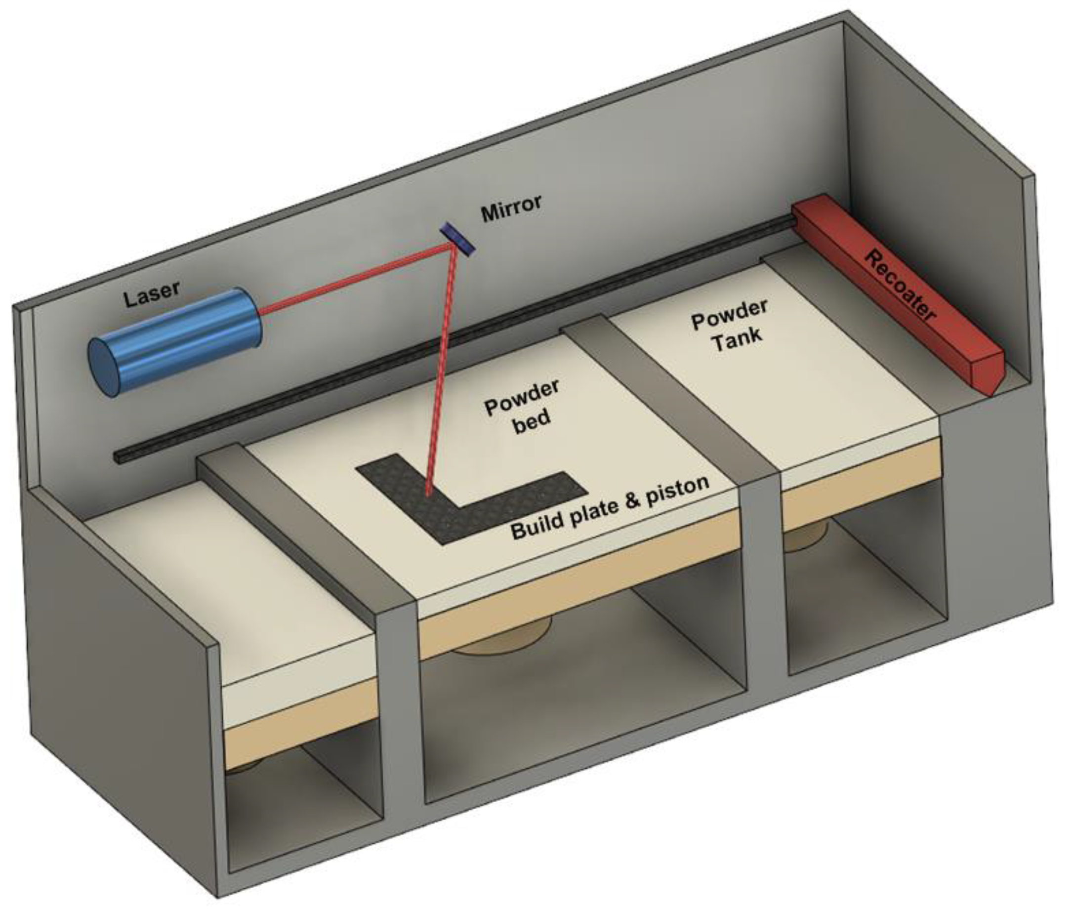
2.1. Experimental Procedures

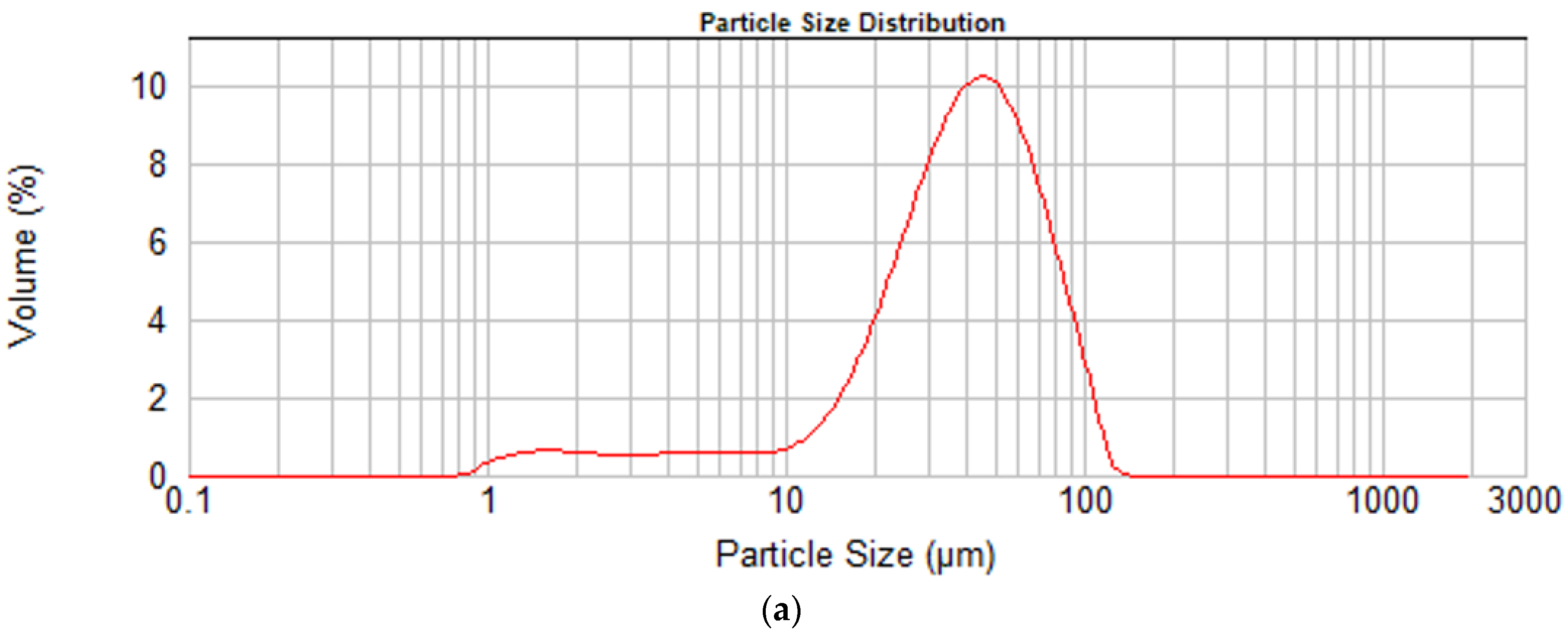
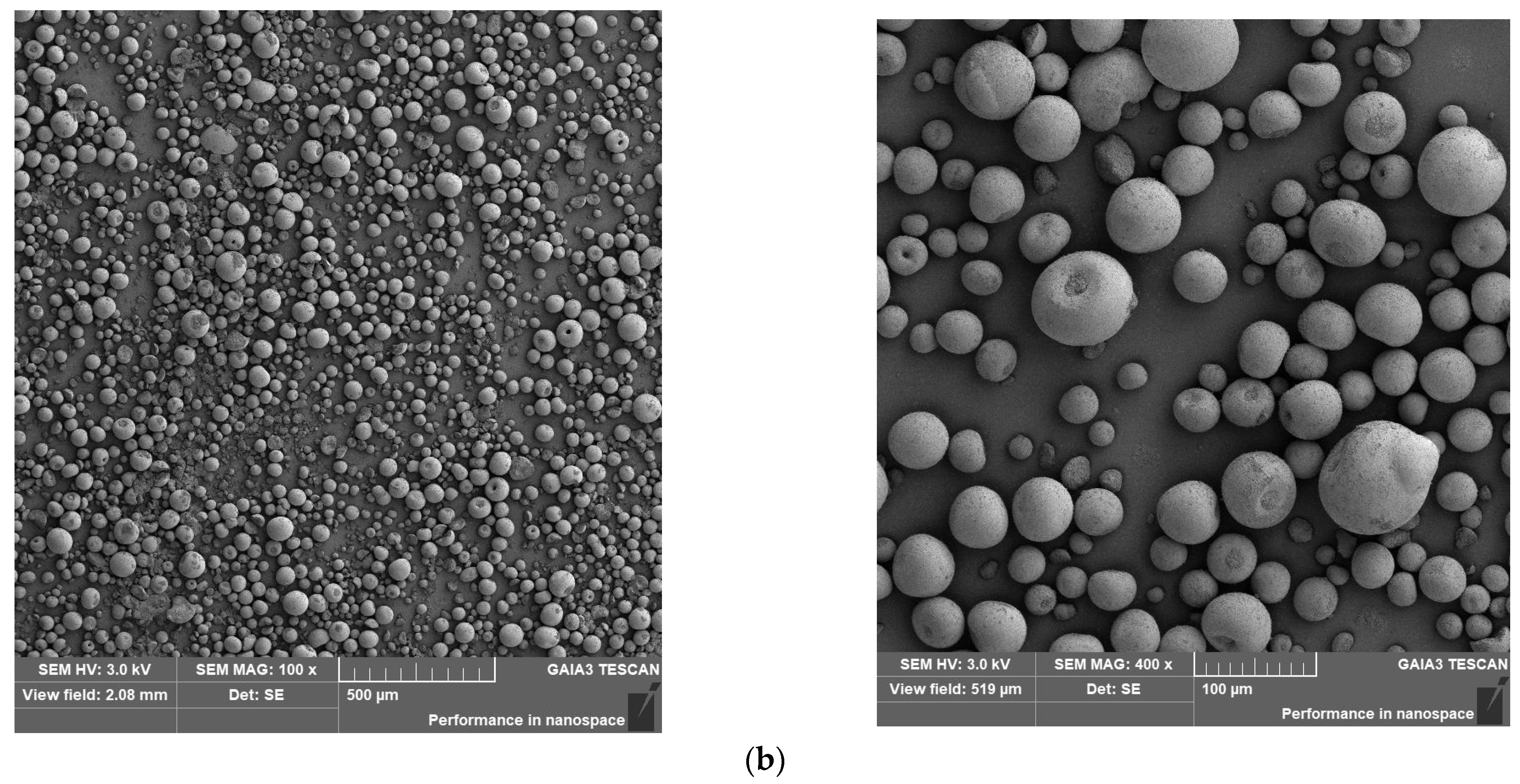
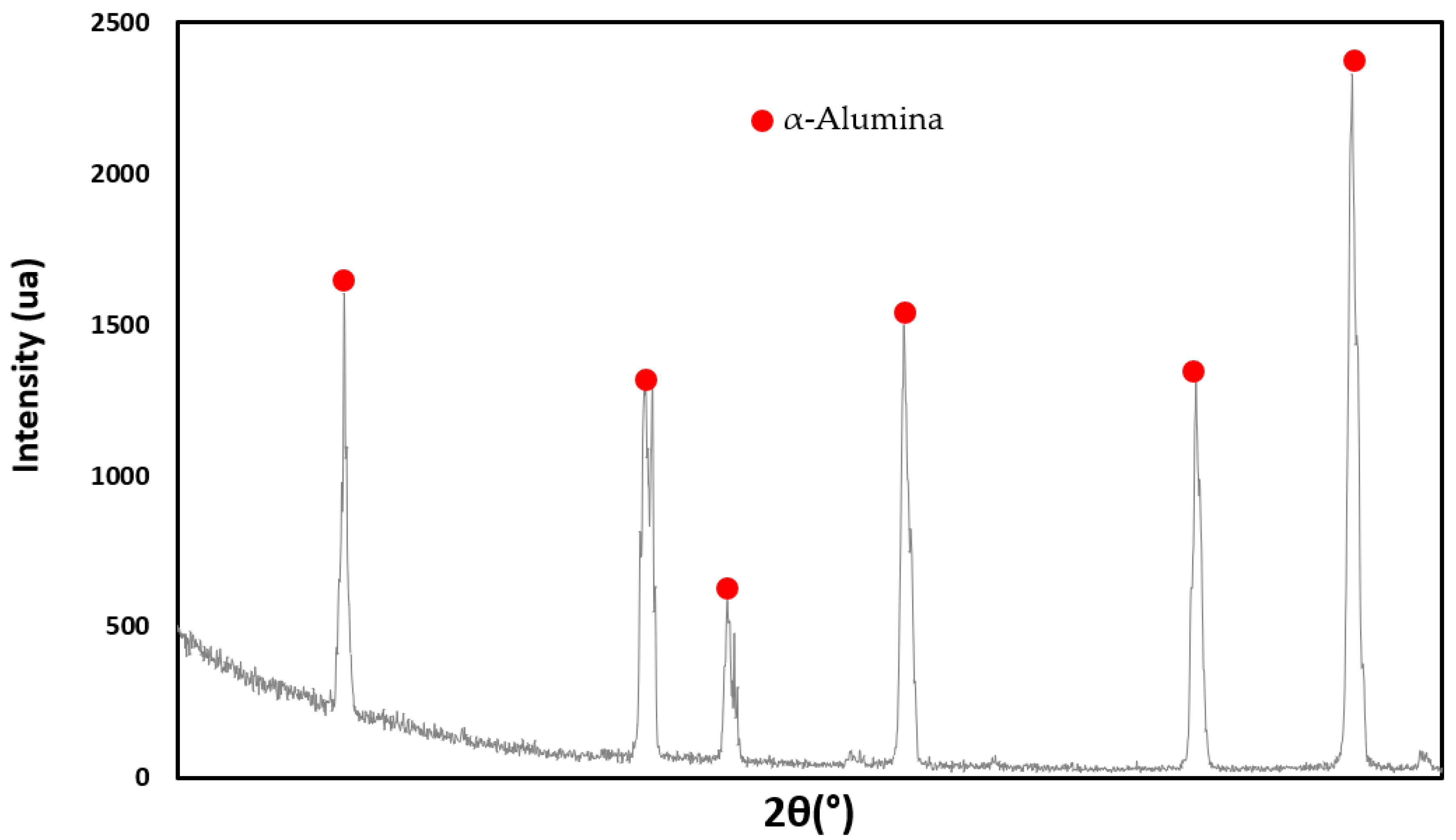
2.1.1. Feedstock Material

The alumina powder used in the present work is P172 LSB (α-alumina 99.7% purity) from Alteo. This raw powder was spray dried from a slurry containing 0.1 vol% of colloidal graphite to increase the powder interaction with the laser. The process used to obtain the alumina feedstock for PBSLP was described in previous work [26]. Flowable spherical powder with d50 = 39.8 μ m was obtained (Figure 2). Beside the optical coupling of the used powder, the fiber laser was enhanced due to the addition of the colloidal graphite [26].

2.1.2. Sample Preparation and Characterization

The Laser Beam-Powder Bed Fusion (LB-PBF) 125 printer manufactured by RENISHAW® and equipped with fiber laser (with a wavelength of 1070 nm, maximum power of 200 W, and a variable spot size) was used to print the alumina samples. The laser spot size of 70 μm and layer thickness of 100 μm were selected for all samples. Six scanning strategies were investigated in this study, as illustrated in Figure 3. An alumina-based material was used as a base plate. Cubic alumina samples (10 × 10 × 10 mm3) were printed to investigate the effect of scanning strategies.

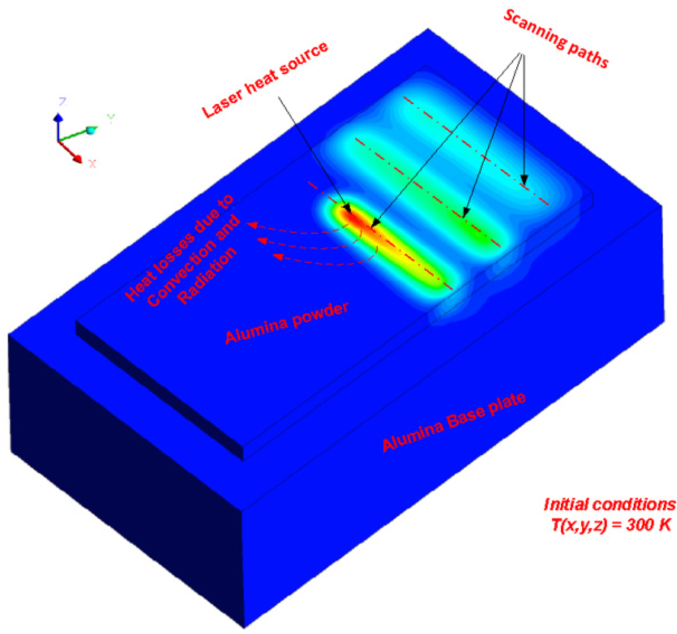
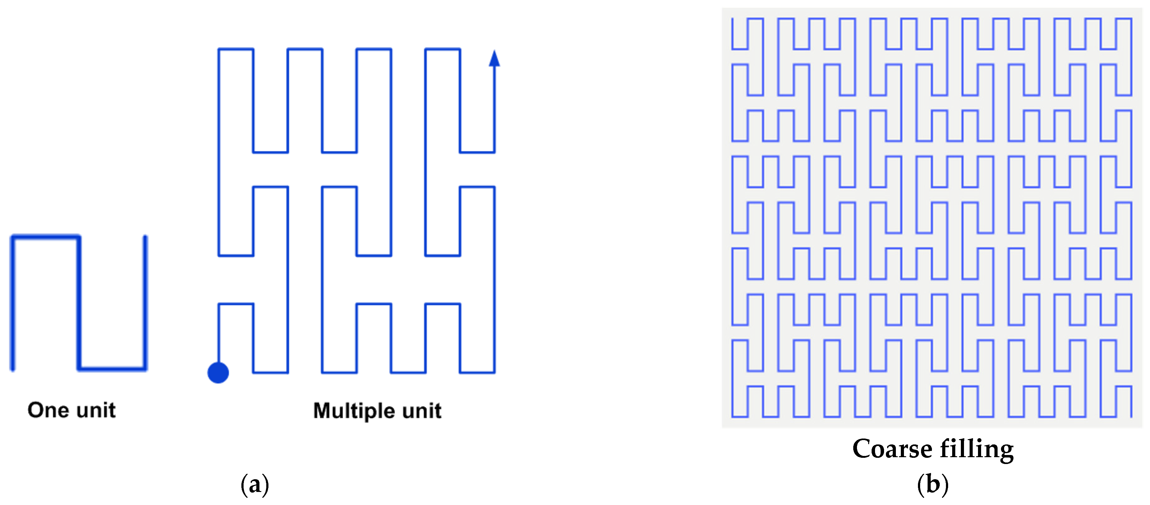
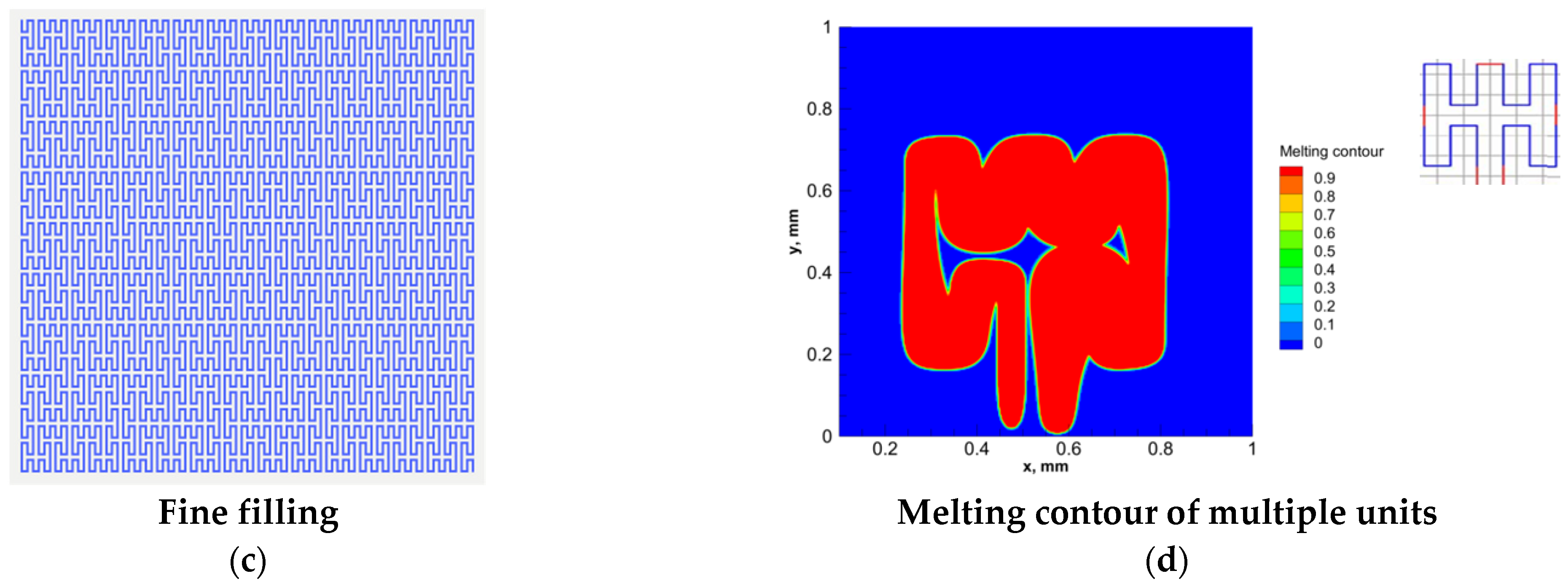
2.2. Numerical Procedures

When the laser beam scans the powder with specific power and speed, a part of the laser beam power is back-scattered into the printer chamber, and the powder absorbs the remaining laser beam to form the melt pool. The powder’s melting is considered a complex process, and it is a challenge to be mathematically modeled. Therefore, the following assumptions were considered: (1) the laser beam has a uniform heat distribution, (2) the molten pool has a flat top surface, (3) the powder bed has a homogeneous and continuous medium, (4) no heat loss due to evaporation. In PBSLP, there are three heat transfer mechanisms: thermal conduction, radiation, and convection. The developed thermal model considered all these mechanisms.

Numerical Model Development

When the laser beam scans the powder, heat is transferred to the powder, as described previously. The energy equation (Equation (1)) was used to model this heat transfer according to [34], where ρ ,   C p ,   T , k , and t are the density, specific heat, temperature, thermal conductivity, and time, respectively.
ρ C p T t = . ( k     T ) + S h
The term Sh in Equation (1) refers to the laser heat source per unit volume (W/m3) and a User-Defined Function (UDF) was developed, compiled, and solved using ANSYS FLUENT 2020R1 to model the laser source as described by Equations (2) and (3) according to [34].
S h = β I o α   exp ( α z )
( x     xs     v   t ) 2 + ( y     ys     v   t ) 2   < = R 2
where β, I o , α, v , and R are the material absorptivity, laser intensity, absorption coefficient, scanning speed, and laser radius, respectively. The xs and ys parameters in Equation (3) are the laser spot initial location on the powder bed and were used to control the laser beam movement on the powder bed (scanning strategies). The absorption coefficient was estimated according to [35]. The laser intensity can be calculated according to [34] as follows:
I o = P π   R 2
To model the nature of the laser modulated mode in the LB-PBF 125 printer, the developed UDF considered this mode where the scanning speed was calculated using the exposure time ( exp _ t ) and the point distance ( p d ) according to Equation (5).
v = p d exp _ t
The initial and boundary conditions applied in this study are shown in Figure 4 and described by Equations (6) and (7):
T ( x , y , z ) t = 0 = T O
k ( T z ) = S h ˙ h c o v ( T a T s ) σ ε ( T a 4 T s 4 )
where T a is the ambient temperature, T s is the powder surface temperature, σ is the Stefan–Boltzmann constant, ε is emissivity, h c o v is the convection coefficient.
Alumina material properties (the effect of colloidal graphite on the material properties was ignored since it is only 0.1 vol%) as a function of temperature (as described in Table 1) and other constants, according to [36], were considered in the developed numerical model and included in the developed UDF. Additionally, the UDF considered the phase transformation from solid to liquid and liquid to solid based on the latent heat of melting. User Defined Memory (UDM) available in ANSYS FLUENT was used to monitor the molten region during the movement of the laser.

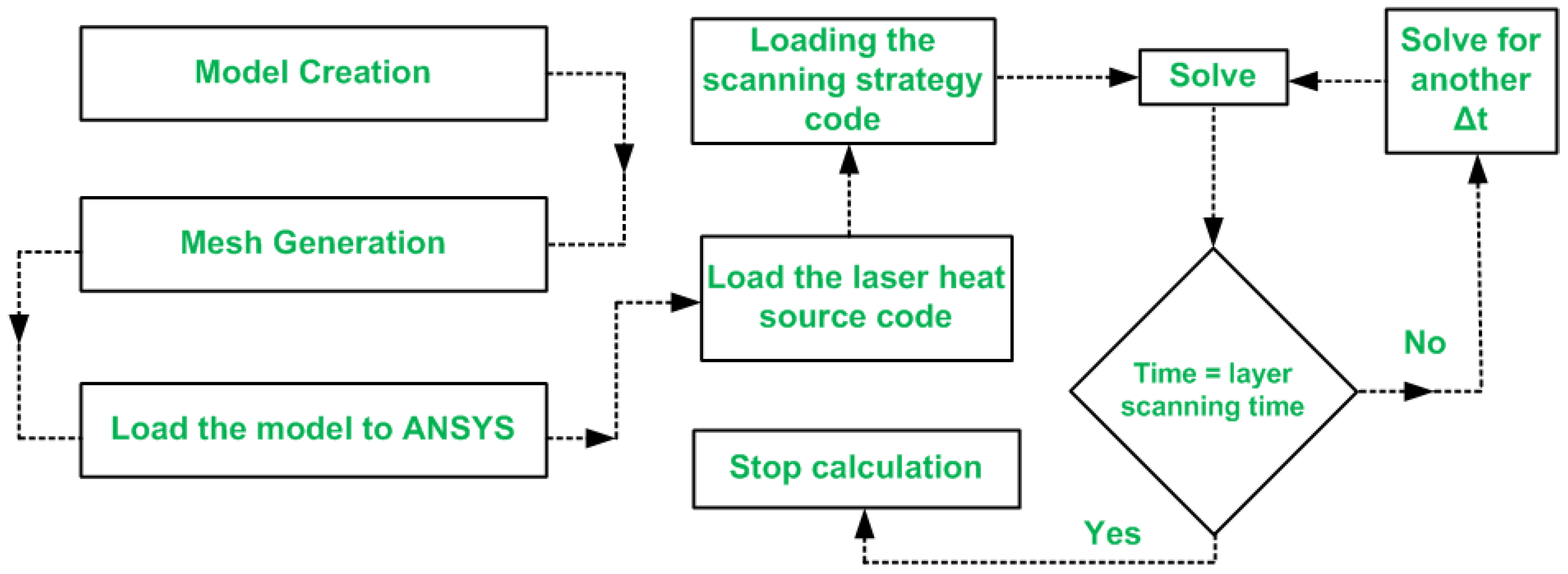
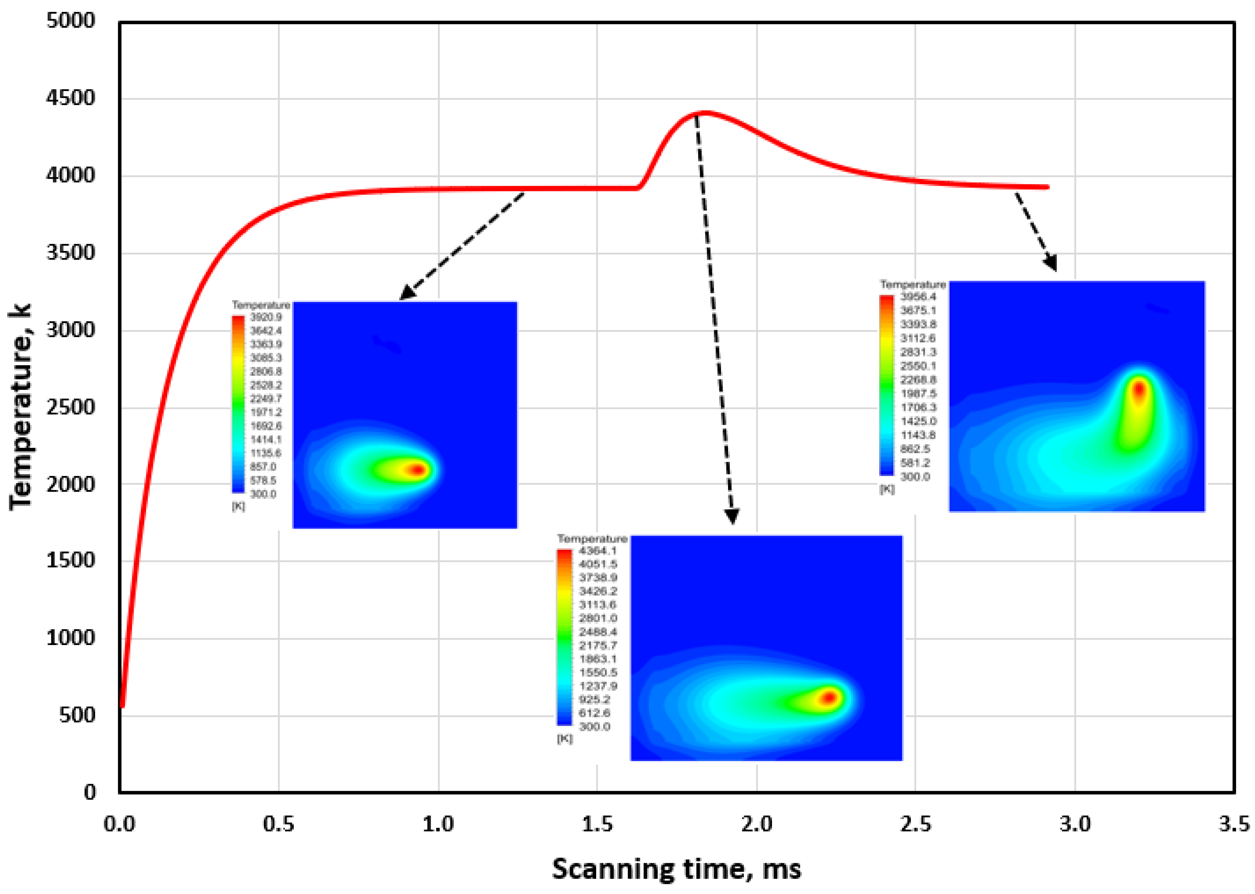
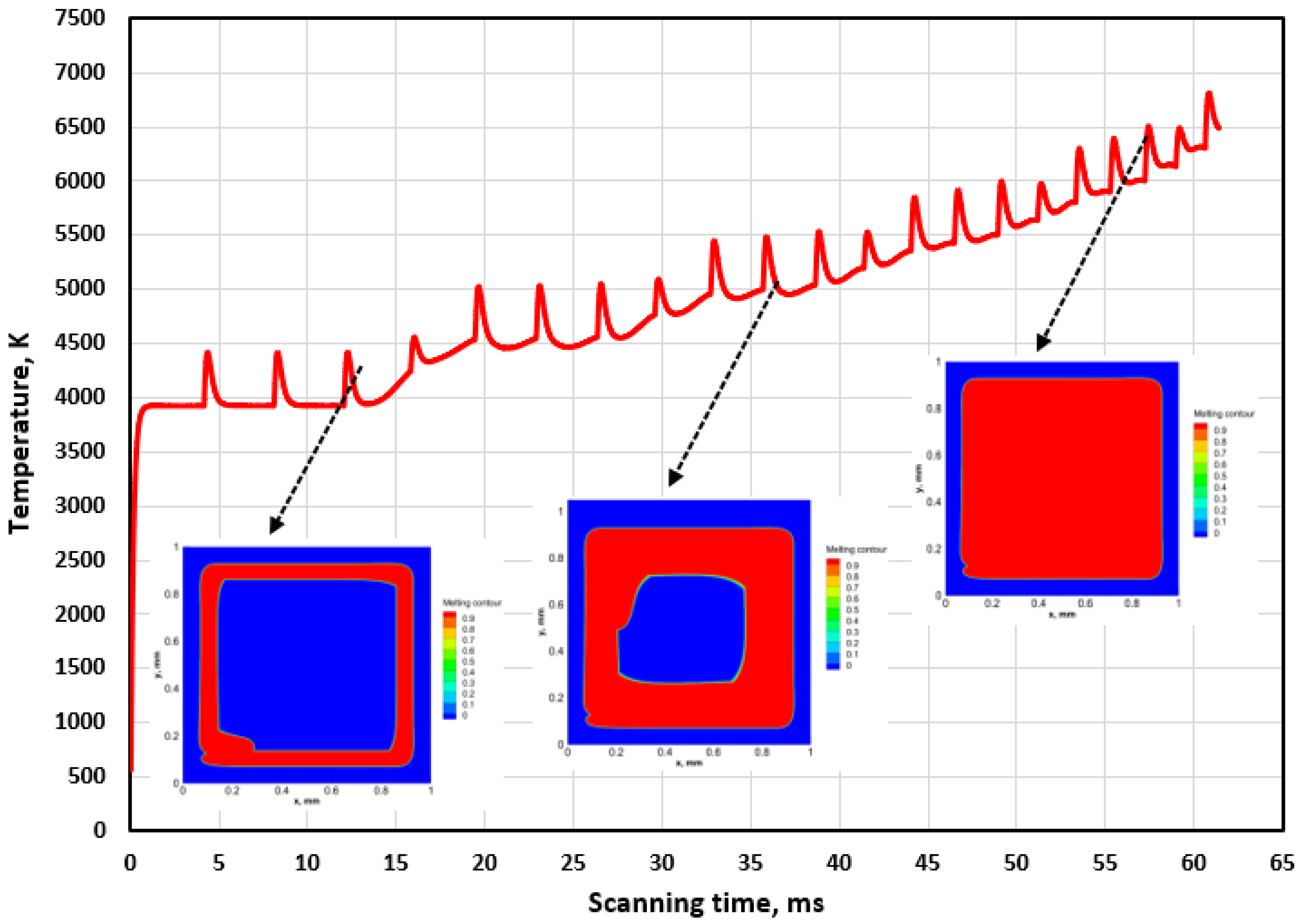
3. Numerical Solution

This section describes the model geometry, the computational domain used in this study, and the numerical solution procedures of the governing equations. Additionally, the verification of the results from the model with experimental data is shown.

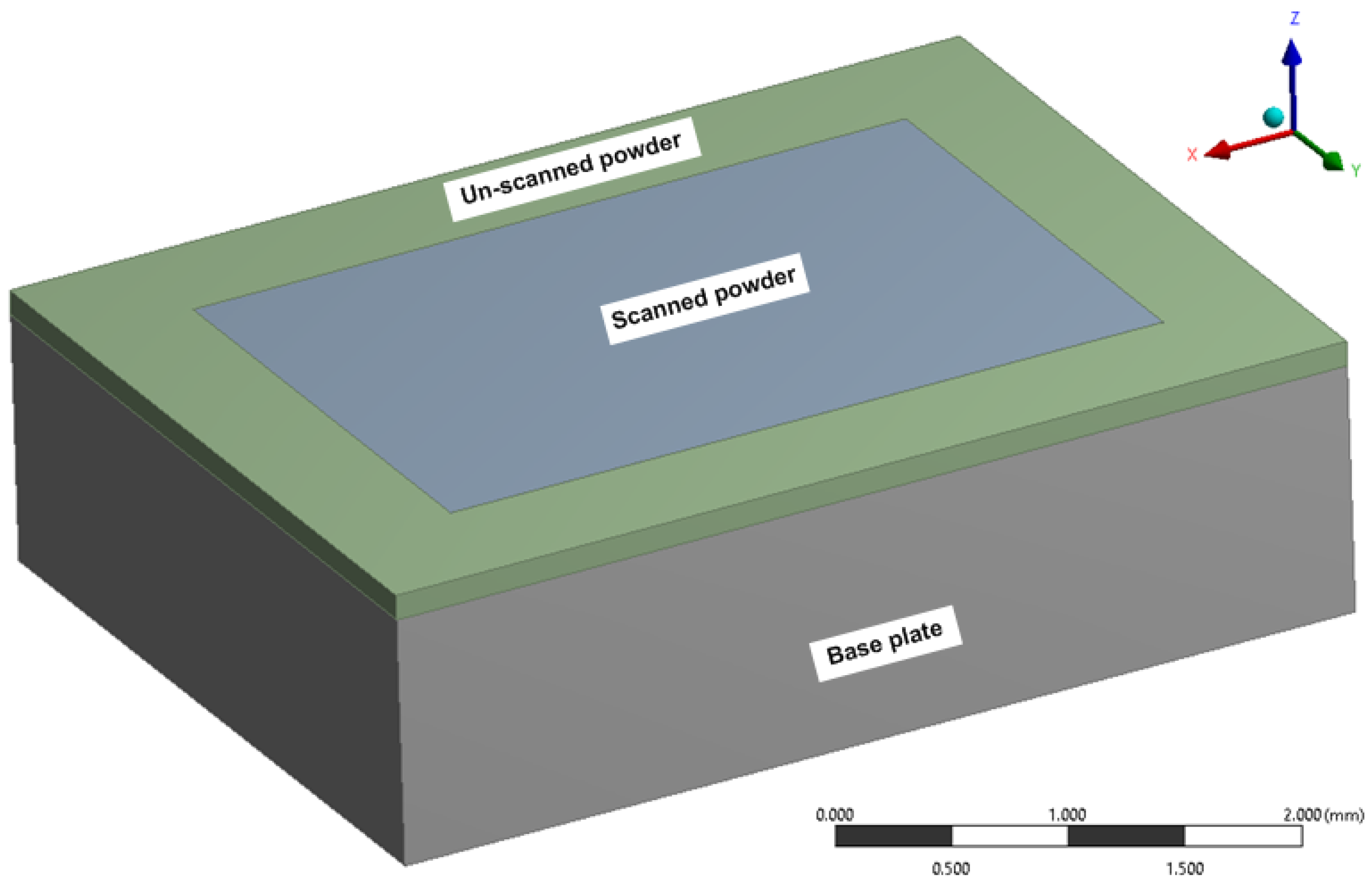
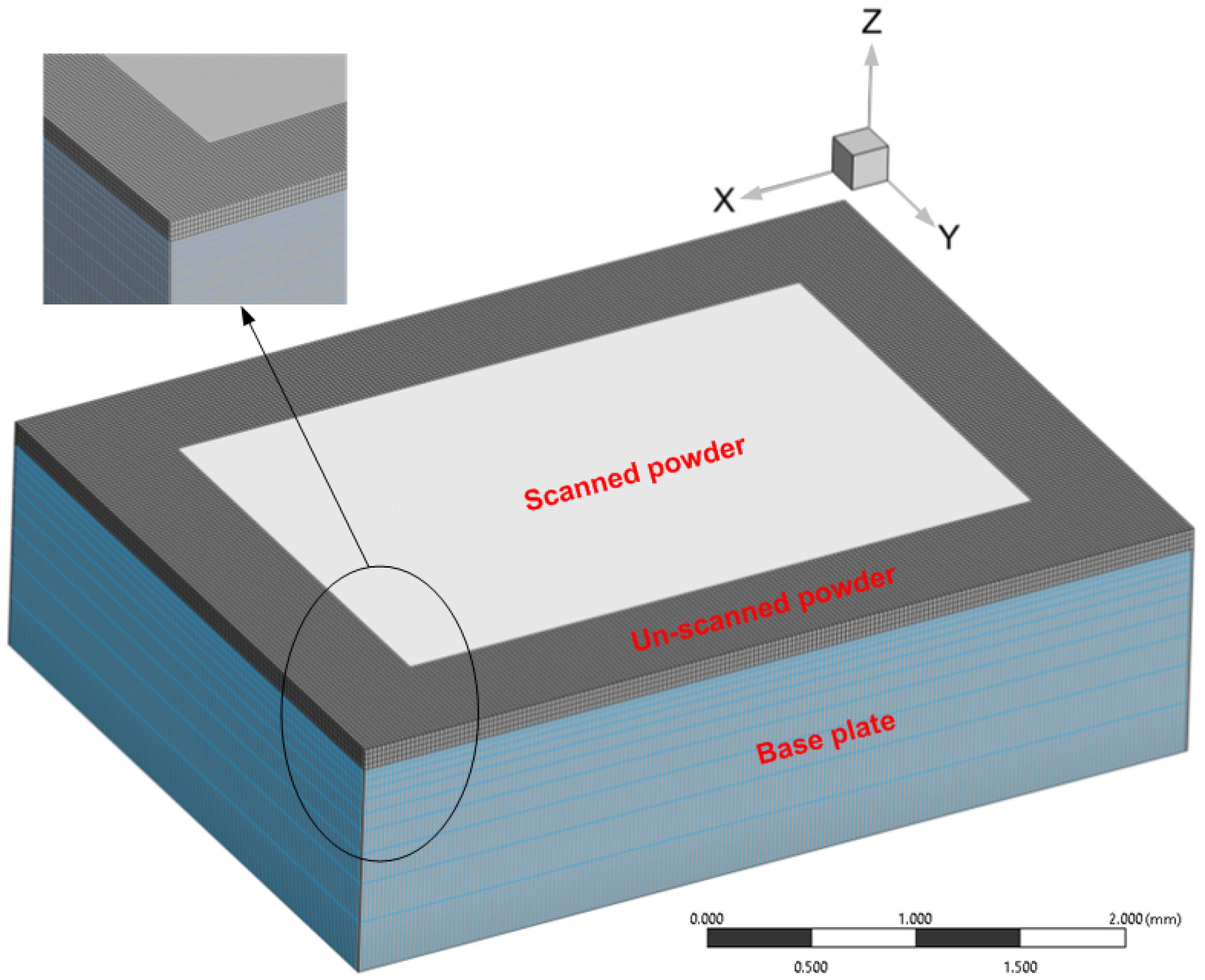
3.1. Model Geometry and the Computational Domain

The physical model used in this study is shown in Figure 5, and its dimensions are summarized in Table 2. The model consists of three main parts: the powder layer, baseplate, and the surrounding powder. The powder layer was assumed to be a homogeneous and continuous medium. In order to see the effect of the scanning strategies, only one layer was considered for the numerical simulation, as almost the same behavior would be repeated at the consecutive layers.
The governing equations described in Section 3 were modeled using UDF. All process parameters for alumina PBSLP were defined in the UDF. Figure 6 shows the numerical solution procedure followed during the solution of the numerical model. The mesh structure used in the numerical analysis was very fine discretization for the layer region, while the coarse mesh was chosen for the base plate and the surrounding powder, as illustrated in Figure 7. A mesh density analysis was carried out to avoid any error in the calculation or the results from bad mesh. The mesh density analysis was performed with four different mesh, with sizes of 10, 5, 3, and 2 µm, and the results are summarized in Figure 8. The maximum temperature and melting track depth and width measurements were used as an analysis criterion. It can be concluded from the mesh density analysis test that the temperature, track depth, and width is almost stable with any mesh size after 3 µm, and therefore mesh sizing of 2 µm was used in this study. Additionally, it is worth mentioning that all measurements were performed when the laser beam temperature became stable.

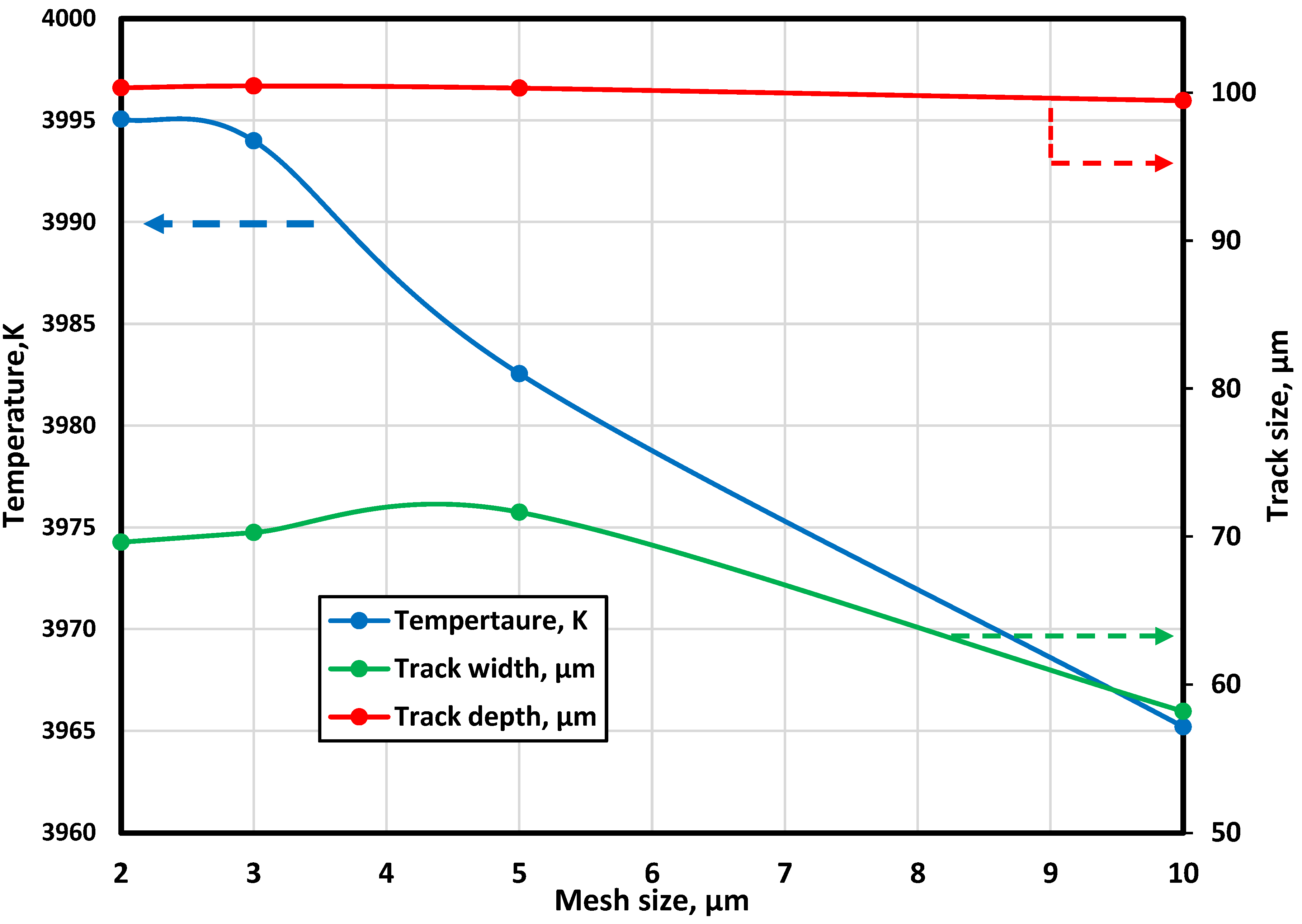
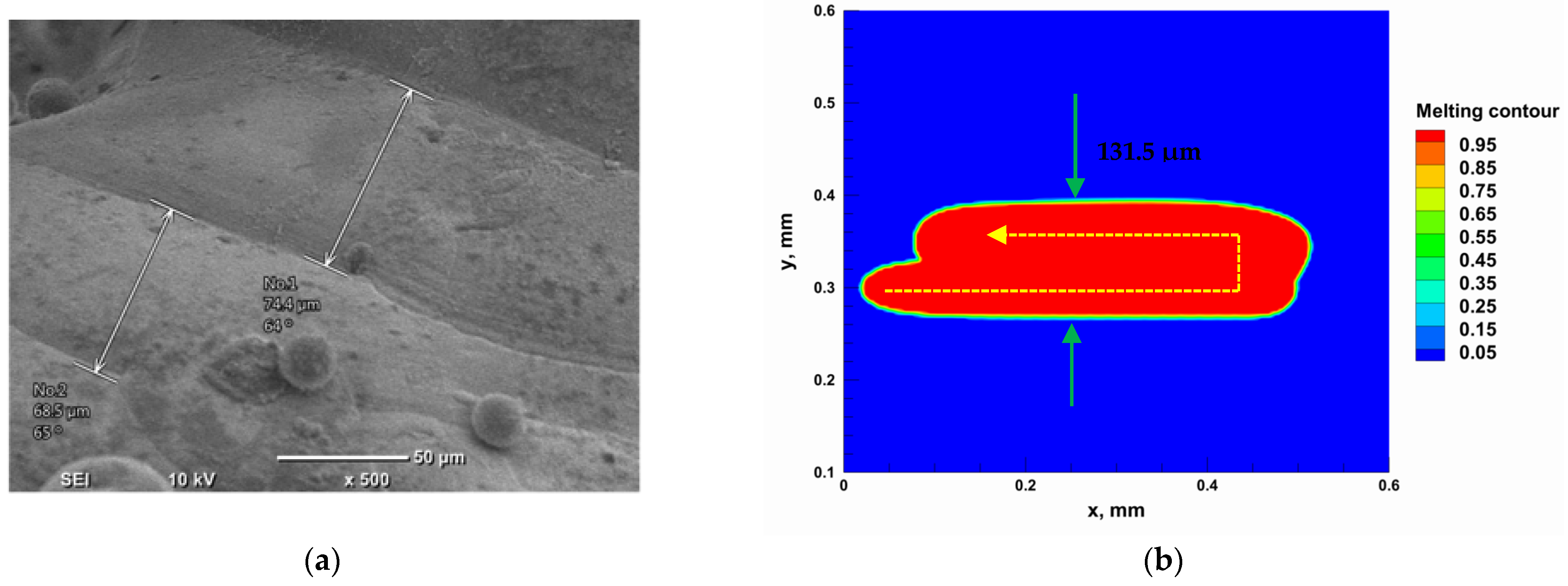
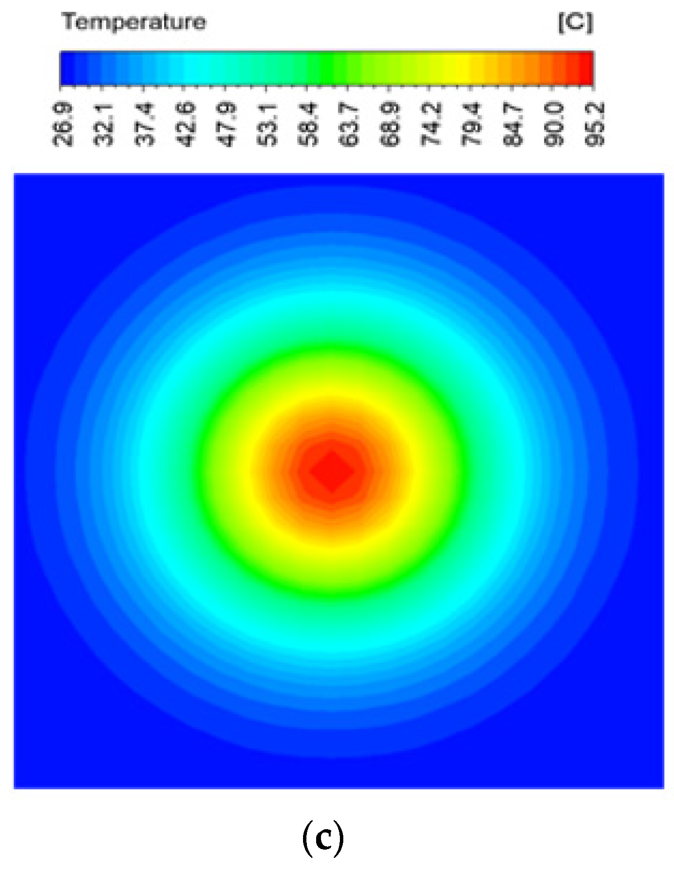
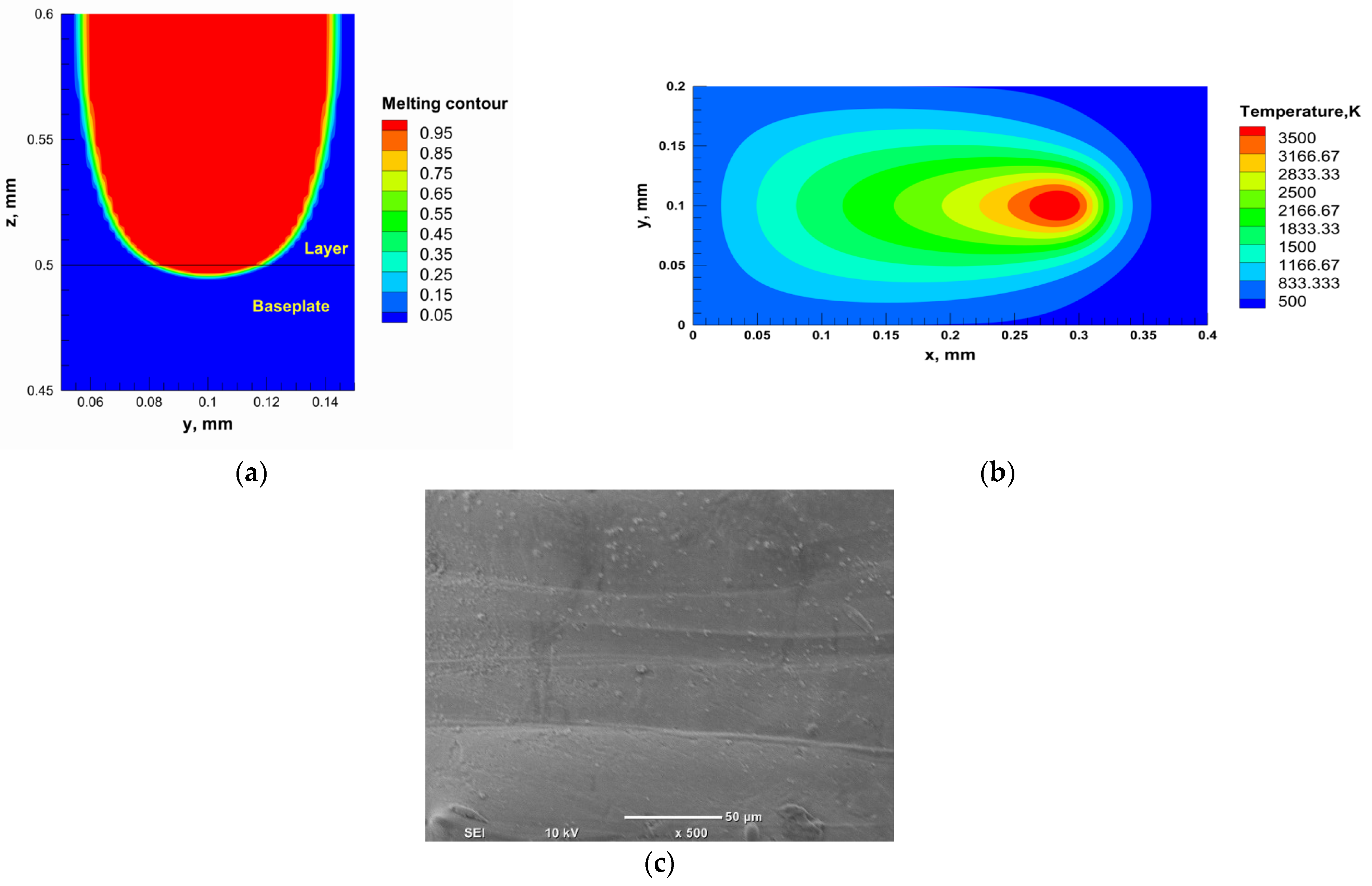
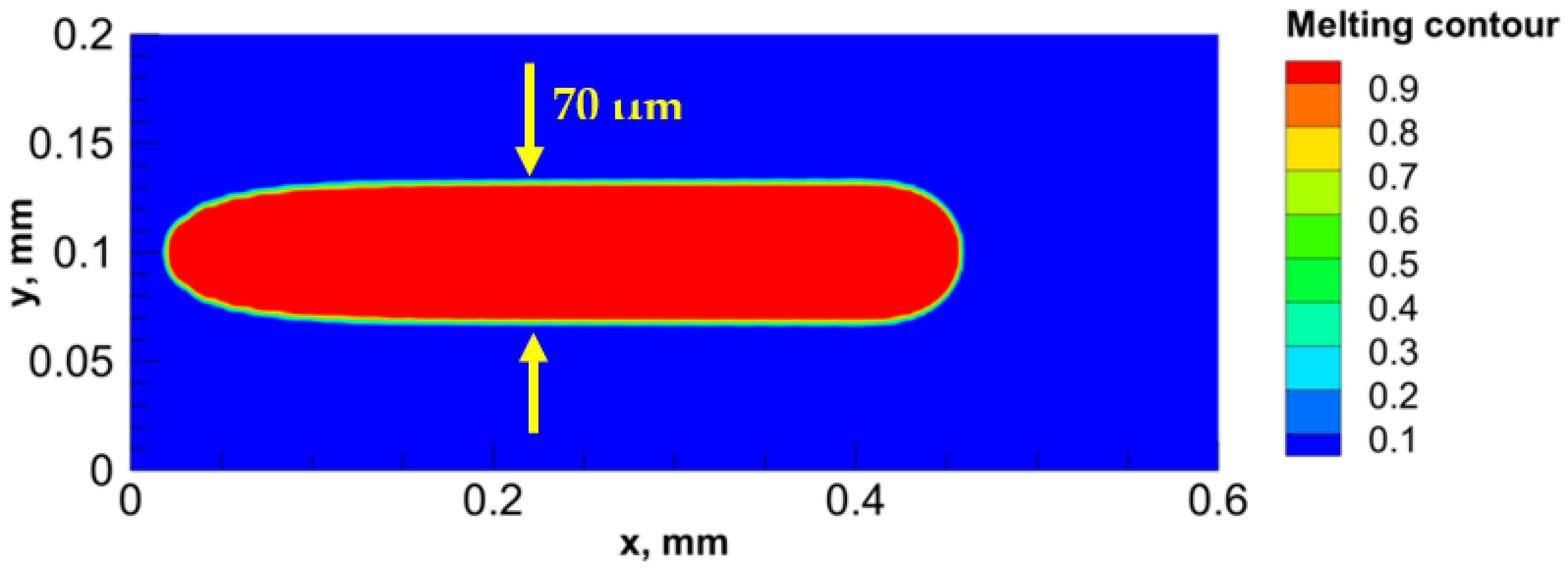
3.2. Model Validation

To ensure the numerical model was validated with experimental results, the numerical melting path width was compared with the experimental melting path width. Experimental and numerical stu1dies were carried out for validation by using 95 W laser power, 100 µm layer thickness, scanning speed 200 mm/s, 50 µm hatching distance (the process parameters used in the validation were initially obtained from the numerical model). Figure 9a,b shows the melt path width analyzed numerically with the same parameters as the melt path width measured in the SEM image of the experimentally produced sample.
Two adjacent melting path widths were measured using SEM analysis where it recorded 142.9 µm. The numerical model was run to make two adjacent paths using the same conditions, which were used experimentally. It gave a width of 131.5 µm for two adjacent melting paths which are close to the experimental results with a calculation error of 8%. It can be concluded that the numerical model is validated with experimental results and can give close results and be used in the analysis.
In addition, experimental and numerical studies were also confirmed by considering the temperature distribution. The temperature contour for the laser spot obtained from the simulation was compared with experimental data. This experimental data is a contour of temperature distribution for a laser spot. The spot was measured using a TVS-2300ST thermal camera manufactured by Avio Nippon Avionics Co., Ltd. [37,38]. The results indicated a perfect similarity between the two results with a calculation error of 1.24%.

4. Results and Discussion

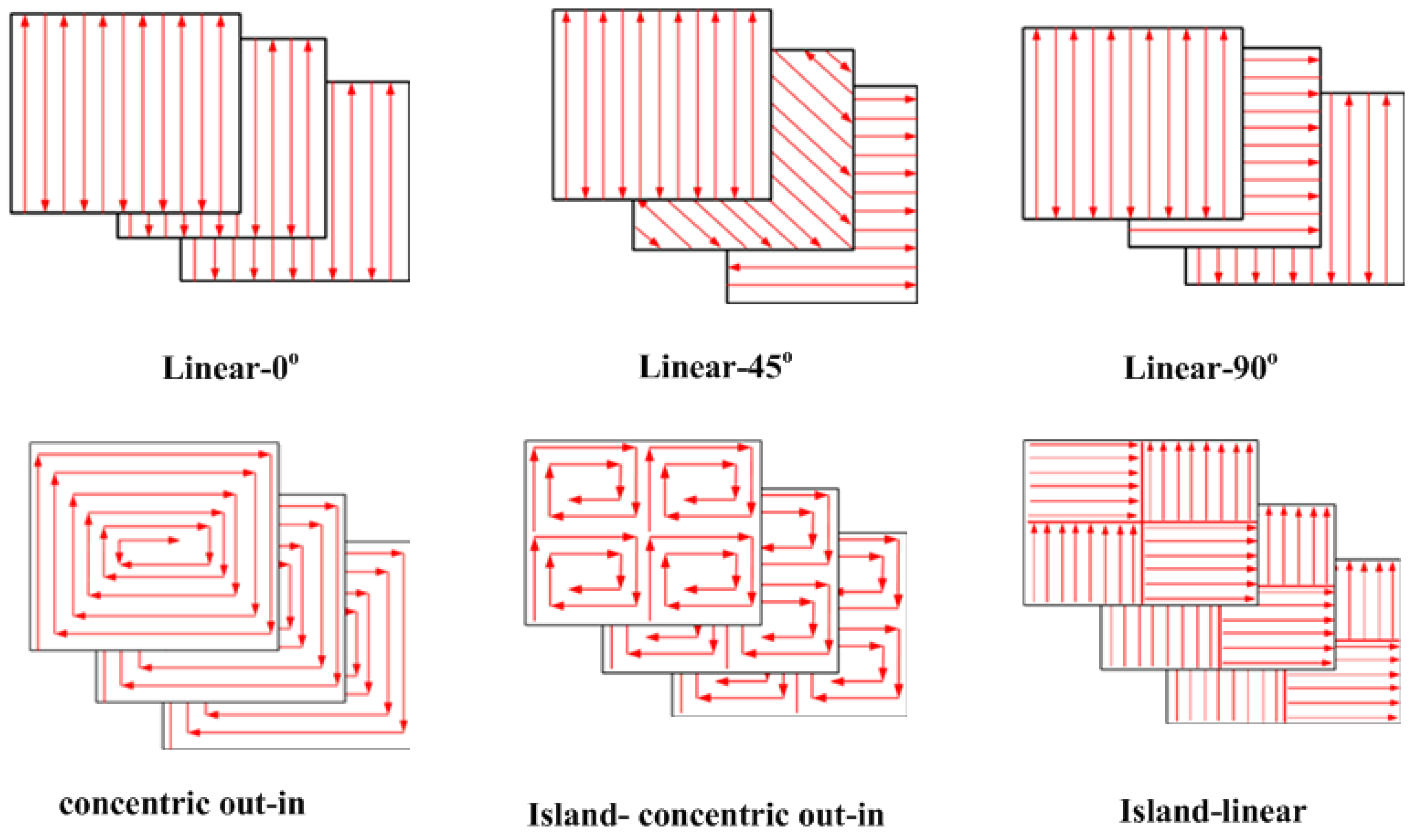
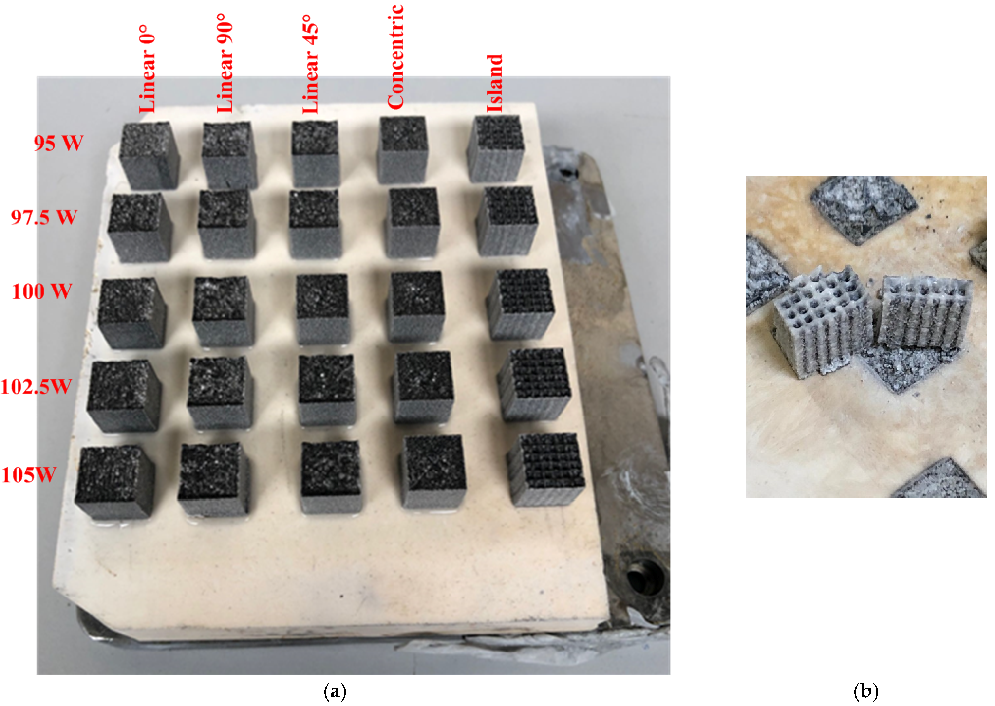
4.1. Process Parameters Selection

It is essential to select the laser power and scanning speed in the range that can melt the layer thickness and adhere it with the previously scanned layer to study the effect of scanning strategies properly. Additionally, at the same time, the generated temperature should be in the acceptable range above the melting point and not evaporate the entire scanning path. In this study, the developed numerical model was used to test different laser powers and scanning speeds until they reached the values that came up with the conditions mentioned earlier. Using laser power 95 W with scanning speed of 200 mm/s was found to melt the whole layer thickness (100 µm) and gave suitable temperature distribution that did not affect the top surface due to high excess heat input (Figure 10a,b). Figure 10c shows the SEM image of the alumina sample top surface printed using 95W and 200 mm/s where no defect can be seen due to high input heat. It was concluded that using a laser power of 95 W and a scanning speed of 200 mm/s is suitable for analyzing the effect of the scanning strategies.
Hatching distance is a critical process parameter as it controls the contact between the adjacent scanning paths and affects the mechanical and physical properties. Therefore, it is crucial to choose the most appropriate hatching distance for alumina’s PBSLP. It was concluded that hatching distance should be selected below 70 µm to ensure that adjacent paths are connected because the width of the melting path is about 70 µm measured numerically as can be seen in Figure 11. Thus, three different hatching distance cases were studied, such as 50, 40, and 30 µm, as shown in Figure 12. By using a hatching distance of 30 µm, it was found that the alumina specimen was destroyed entirely due to the high heat accumulation that resulted from a small hatching distance because the laser source, in this case, scans almost the same position two times. Alumina samples were produced when the 40 µm hatch distance was selected. However, high distortion occurred, especially at the sample base, due to the significantly increased thermal stress due to high temperatures. A full-size alumina sample was able to produce without any problems using a 50 µm hatching distance. Therefore, it is recommended to use a hatching distance of 50 µm. Otherwise, when a more considerable hatching distance is used, discrete scanning paths may occur.

4.2. PBSLP of Alumina Samples

Alumina samples were printed using 95 W laser power, 200 mm/s scanning speed, 50 µm hatching distance, 100 µm layer thickness for different scanning strategies as seen in Figure 13. The sample printed using island-linear strategy was unsuccessful and this was mainly due to the short and adjacent scanning paths that increased the temperature highly at the small island. All other samples have a precise cubic shape (10 × 10 × 10 mm3) with flat surfaces except the top surface. The top surface mirrors the used scanning strategy. The scanning strategies traces are significantly pronounced at the concentric strategy and island strategy. The concentric strategy has two crossed lines making an “X-shape” on the top surface, while the island strategy has small holes on the sample top surface distributed at each island center.
The top surface pattern for all scanning strategies except island-linear was investigated with a 3D microscope (KEYENCE VR-3000), as seen in Figure 14. An irregular structure was observed on the upper surface of all samples. This situation was attributed to the presence of regional densities resulting from different particle size distributions.
For the concentric in-out strategy, the developed numerical model was used to analyze the two crossed lines formed on the layer top surface. It was found that they were formed mainly due to the rotation of the laser beam because when the laser changed the direction, a sharp increase in the temperature occurred, as shown in Figure 15. The sharp increase in temperature is nearly sufficient to vaporize the material at the laser’s rotational position. In this strategy, the laser direction changes at four points per cycle, and the short scanning paths at the inner cycles cause the heat to be concentrated in a small area. As a result, two diagonal lines and a small hole in the center of the sample are formed. It was evaluated that this critical result can help LB-PBF printer manufacturers to make modifications that prevent the sharp return of the laser beam in such strategies.
For island-concentric out-in strategy, since it consists of a small concentric in-out strategy, small holes are formed in the top layer surface, mainly due to the heat concentration at the minimal area as described previously. Figure 16 shows the melting contour and the temperature history for a tiny island where the concentration of the heat led to high-temperature history at the end of the scanning.

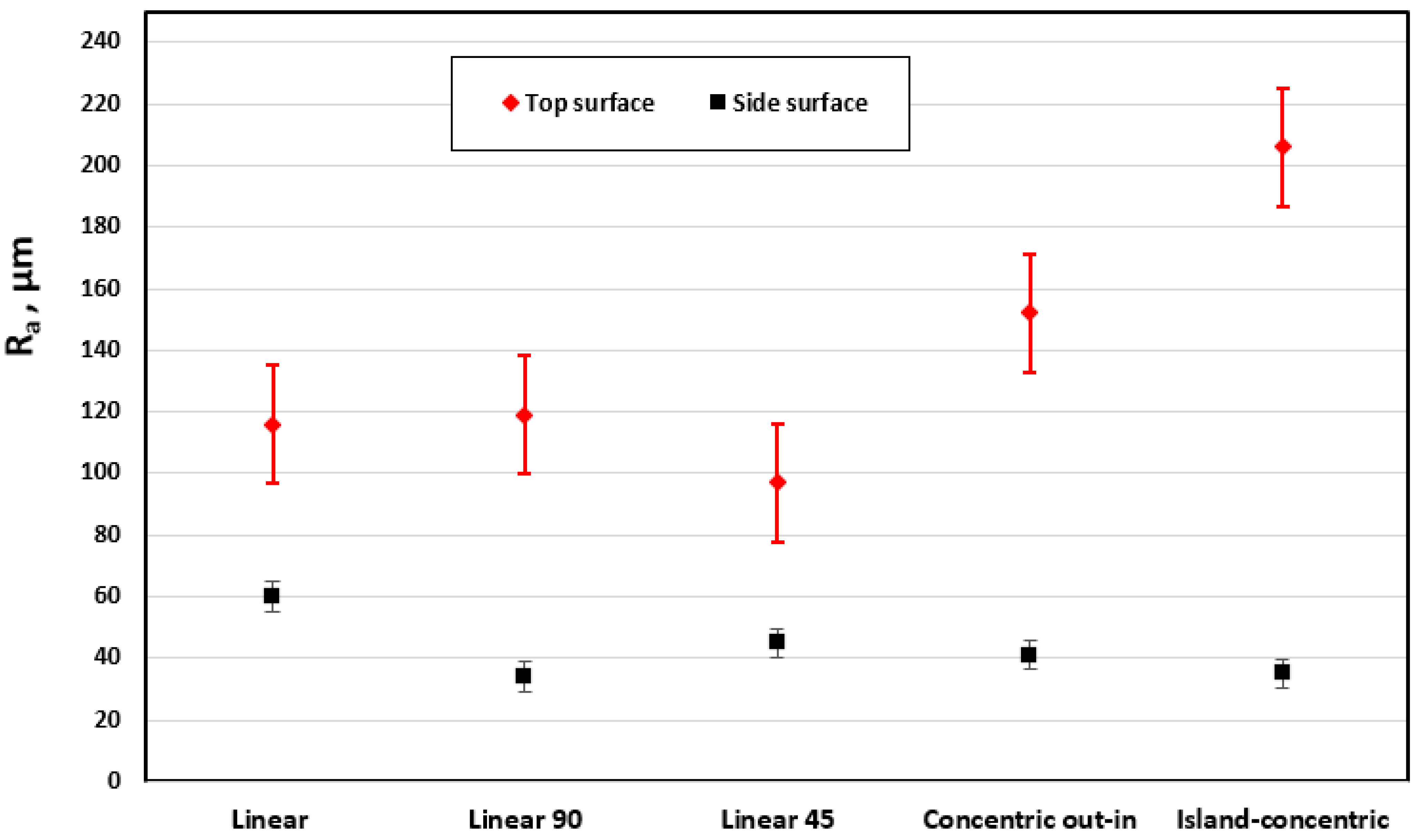
4.3. Surface Roughness

The average surface roughness (Ra) was measured for all samples in the top and side surfaces using the 3D microscope (KEYENCE VR-3000), considering different orientations, and the results are summarized in Figure 17. Generally, the surface roughness values at top surfaces are higher than the side surfaces, mainly due to characteristic patterns formed on the top surface by the scanning strategy paths. The linear strategies gave the lowest surface roughness for the top surface compared to the concentric and island strategies. The surface roughness of 116, 119, and 97 µm was achieved using linear-0°, linear-90°, and linear-45°, respectively. The concentric out-in strategy gave a surface roughness of 152 µm, while the island strategy gave a high surface roughness of 206 µm. The high surface roughness obtained using concentric and island strategies is mainly due to the unique characteristic pattern of the top surface, as described in Figure 14.
For side surface roughness, all scanning strategies gave close values, and the maximum was detected using the linear-00 strategy. Both concentric and island strategies gave low surface roughness, and this is because there is no change in the layer orientation during building (Figure 17).

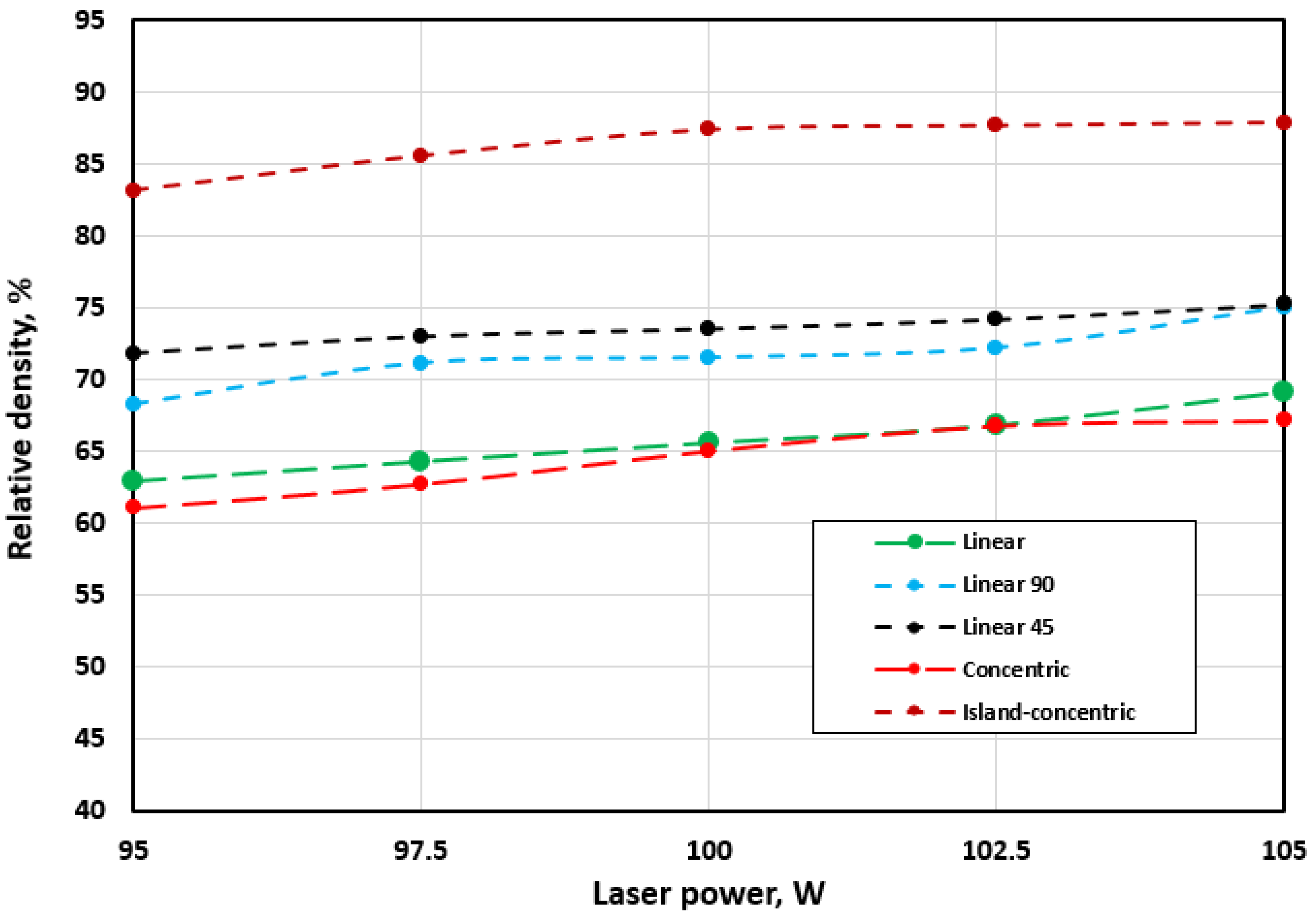
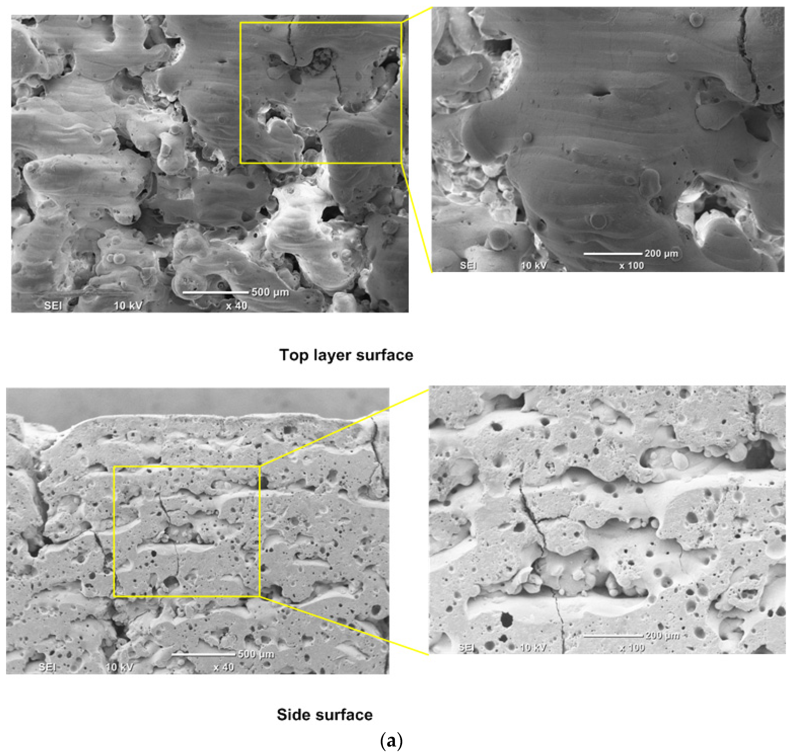
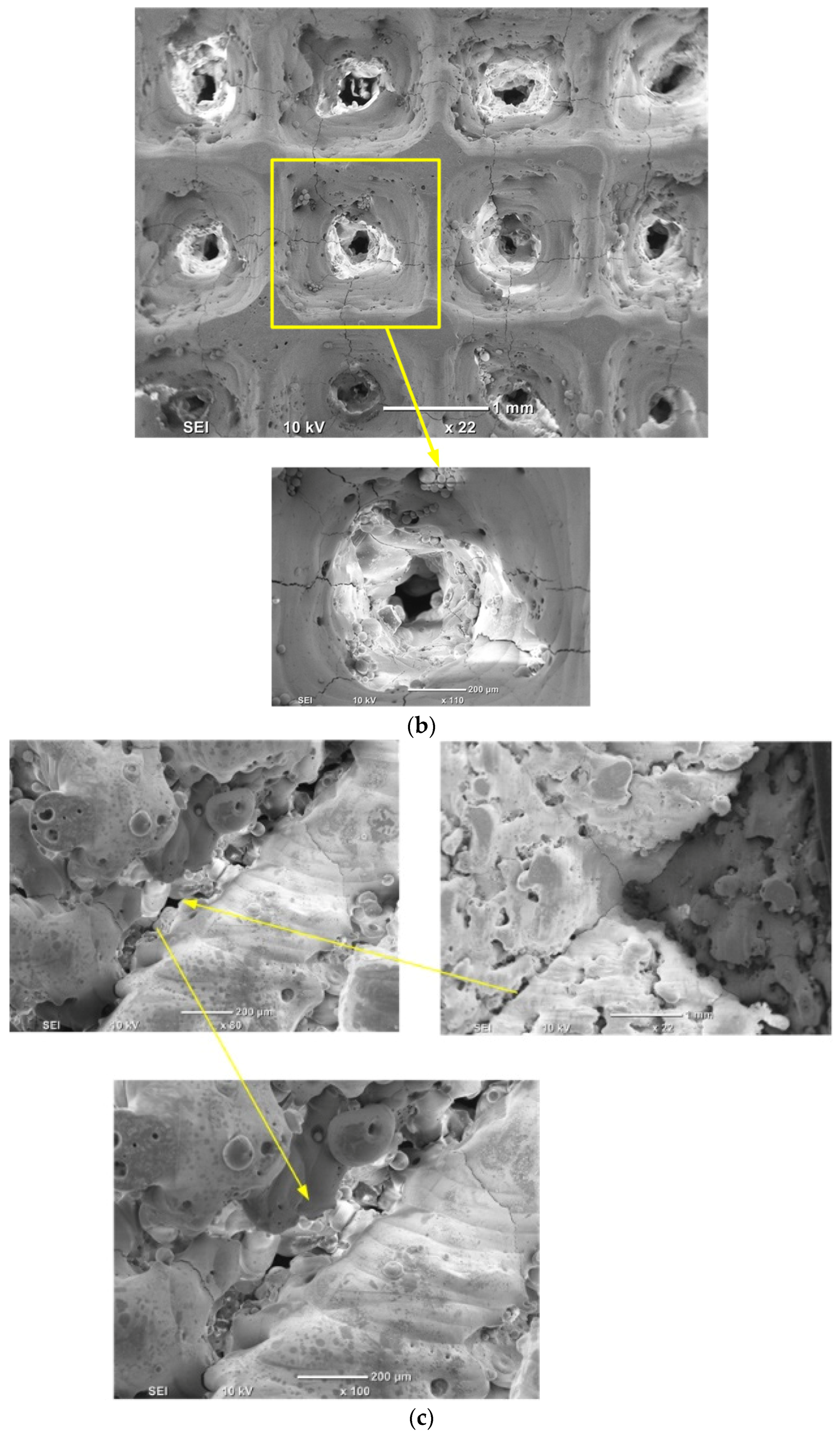
4.4. Relative Density and Microstructure

The Archimedes method was used to measure the relative density of alumina samples produced with different scanning strategies. Different alumina samples were printed using different laser power ranging from 95 W up to 105 W, 200 mm/s scanning speed, 100 µm layer thickness, and 50 µm hatching distance as shown in Figure 18a. Alumina samples have a black-colored surface resulting from the graphite which was added to increase the absorptivity of the powder.
It is worth mentioning that no alumina secondary phases were formed because of graphite addition, which was reported by Juste et al. [26]. For confirmation, XRD analysis was performed for the alumina sample, and that only the alpha-alumina phase existed (Figure 19). Figure 20 shows the relative density variation with laser power at a constant scanning speed of 200 mm/s and different scanning strategies. For the laser power of 105 W, the lowest relative density was obtained at linear-0° and concentric strategies, 69% and 67%, respectively, while for the island strategy, the highest relative density was 87.8 %. Both linear-90° and linear-45° resulted in an excellent relative density that reached 75%. The low relative density obtained using the linear-0° strategy can be explained by no change in the layer orientation, which led to a high porosity level inside the sample comparing to linear-90° and linear-45°. The low relative density obtained at the concentric strategy is the result of the evaporation of material during the laser rotation. The island strategy produced more dense alumina samples than with the other scanning strategies, although small round channels inside the sample as shown in Figure 18b. This can be explained by the high concentration of heat resulting from the short scanning paths in tiny areas (islands), which increased the densification. However, these small channels remain an obstacle for this strategy to be of practical usage for PBSLP of alumina, and modifications are needed to avoid these holes. Furthermore, it can be noted from Figure 20 that the relative density increases with the increase in the laser power due to high energy density, which leads to more dense alumina tracks.
Figure 21 shows the SEM images of the studied scanning strategies, using the same process parameters, such as linear 0°, concentric, and island-concentric out-in strategy. For linear-0°, as shown in Figure 21a, the consolidated particles were formed intermittently and unconnected to each other, and this explains the low relative density obtained using the scanning strategy. Many cracks formation can be seen on the layer top surface. These cracks are mainly formed due to thermal shocks, and the initiation of cracks was started from places that did not contain consolidated alumina (pores). The SEM images for the side surfaces also show periodically repeated defects along the build direction resulting from the lack of adhesion between layers in some locations. The SEM images for the island-concentric out-in strategy show the small holes formed at the center of each island (Figure 21b). Cracks starting and continuing from the center of the holes are also observed, which may affect the mechanical properties of the alumina samples. Figure 21c shows the SEM images of the concentric strategy where the two lines from the “X-shape” are apparent. As shown in Figure 21d, the piece was easily broken due to these split lines, which separated the alumina samples into four identical parts.

4.5. Next Generation Scanning Strategy

Based on this study, the island-concentric in-out strategy can be considered an effective scanning strategy, concerning the high obtained relative density provided that the small hole formation at the center of the islands is solved. Generally, the island-concentric in-out strategy uses short scanning paths in a minimal area (island) to concentrate the heat and increase the relative density. Therefore, this paper introduces a new generation of scanning strategy that depends on using small scanning paths but distributed over the powder layer to eliminate the occurrence of small holes formed using the island strategy. The next-generation scanning strategy is based on the space-filling mathematical curves to control the movement of the laser beam on the powder bed. The space-filling curve formed from the 2D unit square, as can be seen in Figure 22a, and the scanning strategy is formed by repetition of this 2D rectangular unit shown in Figure 22b,c. The study proposed this new strategy for future work because of the difficulty of modifying commercial LB-PBF printers’ built-in scanning strategies. Figure 22d shows the melting contour for the newly proposed scanning strategy. The laser makes a short scanning path over a wide area to avoid the concentration of heat in a minimal area, as is the case in the island strategy. Additionally, some missing scanned regions could be covered by controlling the long and short rectangular sides’ lengths.

5. Conclusions and Future Study

Six scanning strategies, linear with different orientations, concentric and island as available in commercial LB-PBF printers, were investigated in this study. The effect of the scanning strategy on the PBSLP of alumina was examined numerically and experimentally. The developed numerical model determined the value of the experimental parameters (laser power and scanning speed) used in this study. The laser power (95 W), scanning speed (200 mm/s), layer thickness (100 µm), and hatching distance (50 µm) were kept constant during the investigation. Full-size ceramic samples were produced. As a result of the detailed research, the following conclusions were reached:
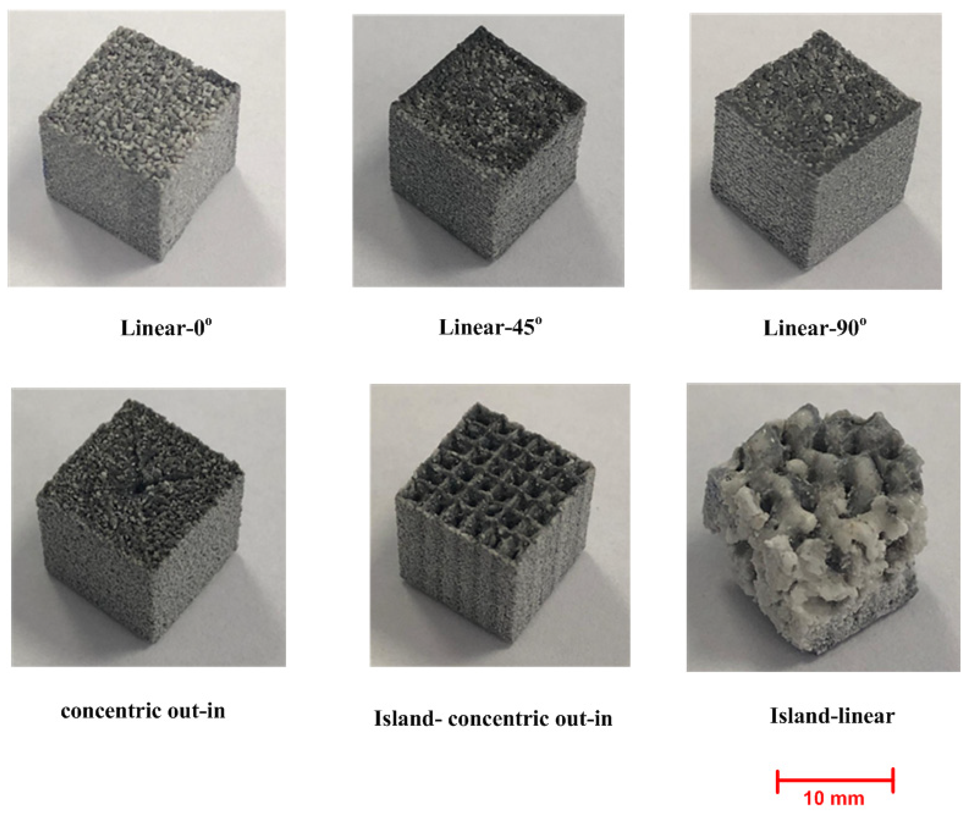
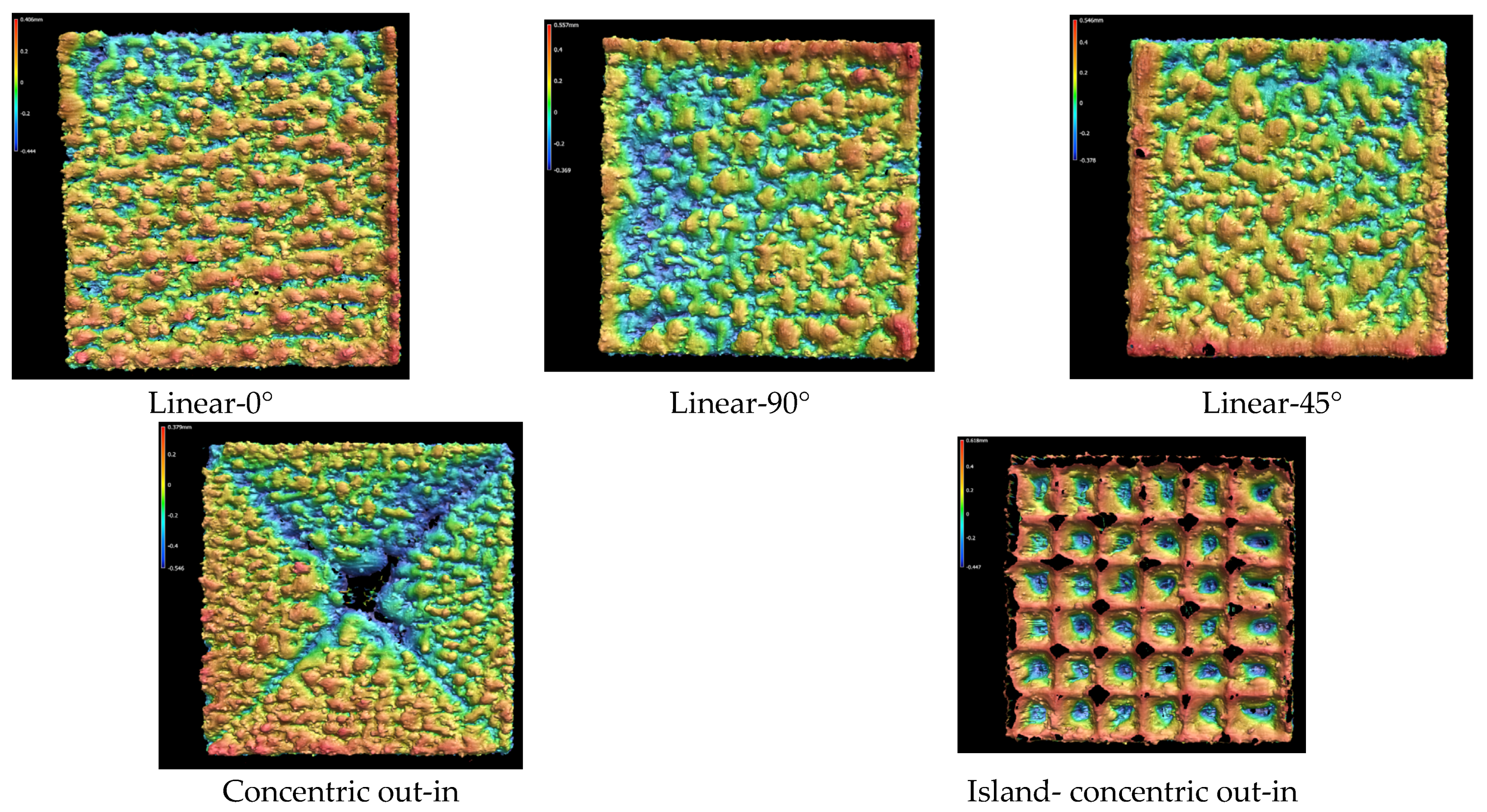
  • Both the island and concentric strategies formed a characteristic pattern on the layer top surface while the linear strategy produced a flat surface. These patterns are considered a problem as they affect the surface roughness significantly.
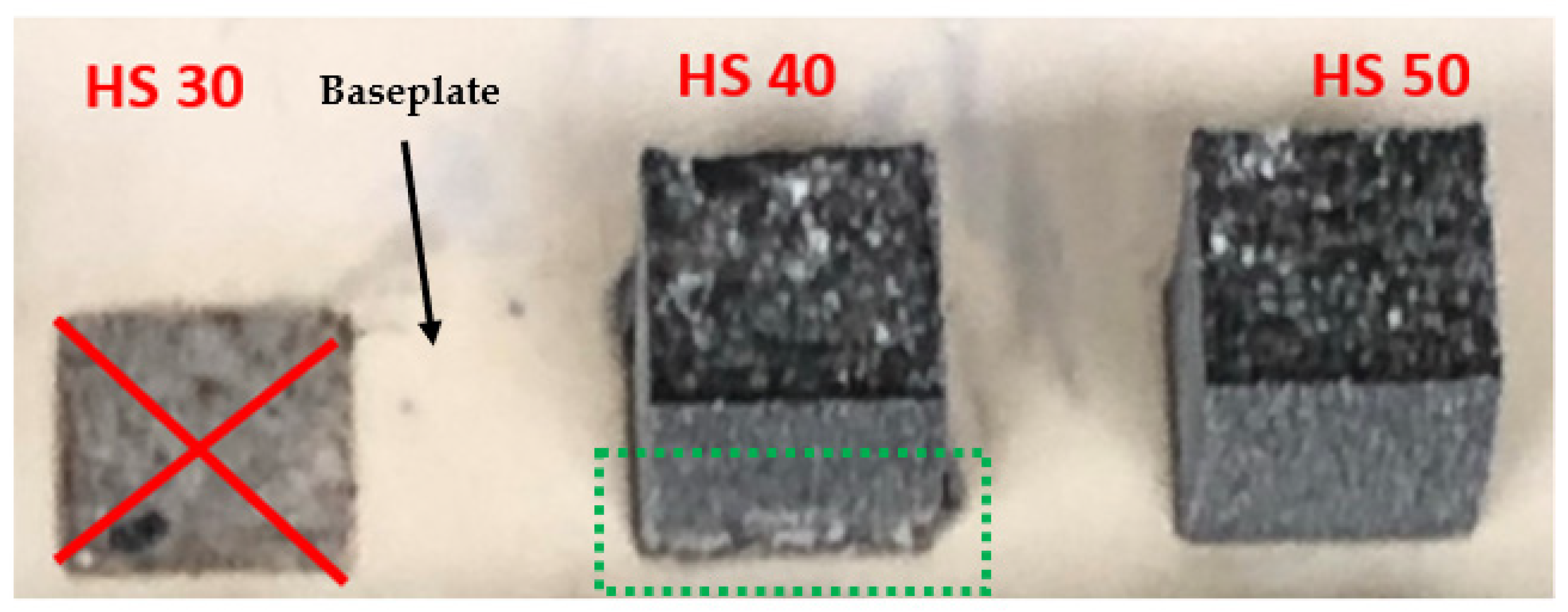
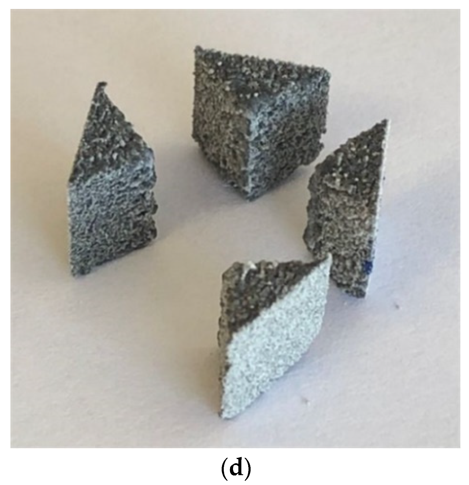
  • The island strategy gave the highest relative density (87.8%) compared to the other scanning strategies, although the round passages formed inside the alumina sample.
  • Linear-45° is considered the best scanning strategy as it succeeded in obtaining an excellent relative density with a flat top and side surfaces.
  • A new scanning strategy needs to be developed for ceramic materials, and this paper proposed a new strategy that may be effective for ceramic materials.
For future study, testing the new proposed scanning strategy should be performed experimentally to examine its effect on the PBSLP of alumina.

Author Contributions

Conceptualization, M.A., G.K., E.J. and F.P.; investigation, M.A.; writing—original draft preparation, M.A.; writing—review and editing M.A., G.K., E.J. and F.P.; supervision, G.K., E.J. and F.P.; project administration, G.K. and F.P. All authors have read and agreed to the published version of the manuscript.

Funding

This project has received funding from the European Union’s Framework Program for Research and Innovation Horizon 2020 (2014-2020) under the Marie Skłodowska-Curie Grant Agreement No. [764935].

Institutional Review Board Statement

Not applicable.

Informed Consent Statement

Not applicable.

Conflicts of Interest

The authors declare that they have no conflict of interest/competing interests.

Ethical Approval

All applicable international, national, and/or institutional guidelines for the care and use of research and materials were followed.

Consent for Publication

Authors give the Publisher the permission to publish the Work.

References

  1. Auerkari, P. Mechanical and Physical Properties of Engineering Alumina Ceramics; Technical Research Centre of Finland: Espoo, Finland, 1996; Volume 26. [Google Scholar]
  2. Fu, L.; Huang, A.; Gu, H.; Ni, H. Properties and microstructures of lightweight alumina containing different types of nano-alumina. Ceram. Int. 2018, 44, 17885–17894. [Google Scholar] [CrossRef]
  3. Hirashima, H.; Kojima, C.; Imai, H. Application of alumina aerogels as catalysts. J. Sol-Gel Sci. Technol. 1997, 8, 843–846. [Google Scholar] [CrossRef]
  4. Kim, J.-H.; Yoo, S.-J.; Kwak, D.-H.; Jung, H.-J.; Kim, T.-Y.; Park, K.-H.; Lee, J.-W. Characterization and application of electrospun alumina nanofibers. Nanoscale Res. Lett. 2014, 9, 44. [Google Scholar] [CrossRef] [Green Version]
  5. Bian, H.; Song, X.; Hu, S.; Lei, Y.; Jiao, Y.; Duan, S.; Feng, J.; Long, W. Microstructure Evolution and Mechanical Properties of Titanium/Alumina Brazed Joints for Medical Implants. Metals 2019, 9, 644. [Google Scholar] [CrossRef] [Green Version]
  6. Steyer, T.E. Shaping the Future of Ceramics for Aerospace Applications. Int. J. Appl. Ceram. Technol. 2013, 10, 389–394. [Google Scholar] [CrossRef]
  7. Alias, S.S.; Harun, Z.; Ismail, N.F. Microstructure and physical characterization of alumina-sintered body via hot isostatic pressing. J. Aust. Ceram. Soc. 2019, 55, 969–975. [Google Scholar] [CrossRef]
  8. Ananthakumar, S.; Menon, A.R.R.; Prabhakaran, K.; Warrier, K.G.K. Rheology and packing characteristics of alumina extrusion using boehmite gel as a binder. Ceram. Int. 2001, 27, 231–237. [Google Scholar] [CrossRef]
  9. Thomas-Vielma, P.; Cervera, A.; Levenfeld, B.; Várez, A. Production of alumina parts by powder injection molding with a binder system based on high density polyethylene. J. Eur. Ceram. Soc. 2008, 28, 763–771. [Google Scholar] [CrossRef]
  10. Tarõ, Á.G.; Ferreira, J.M.F.; Lyckfeldt, O. Infuence of the Stabilising Mechanism and Solid Loading on Slip Casting of Alumina. J. Eur. Ceram. Soc. 1998, 18, 479–486. [Google Scholar] [CrossRef]
  11. ASTM International. Additive Manufacturing—General Principles—Terminology; ISO/ASTM International 52900:2015; ASTM International: West Conshohocken, PA, USA, 2015. [Google Scholar]
  12. Montón, A.; Abdelmoula, M.E.; Küçüktürk, G.; Maury, F.; Grossin, D.; Ferrato, M. Experimental and numerical study for direct powder bed selective laser processing (sintering/melting) of silicon carbide ceramic. Mater. Res. Express 2021, 8, 045603. [Google Scholar] [CrossRef]
  13. Subramanian, K.; Vail, N.; Barlow, J.; Marcus, H. Selective laser sintering of alumina with polymer binders. Rapid Prototyp. J. 1995, 1, 24–35. [Google Scholar] [CrossRef]
  14. Shahzad, K.; Deckers, J.; Boury, S.; Neirinck, B.; Kruth, J.-P.; Vleugels, J. Preparation and indirect selective laser sintering of alumina/PA microspheres. Ceram. Int. 2012, 38, 1241–1247. [Google Scholar] [CrossRef]
  15. Meyers, S. Additive Manufacturing of Technical Ceramics: Laser Sintering of Alumina and Silicon Carbide; KU Leuven—Faculty of Engineering Science: Leuven, Belgium, 2019. [Google Scholar]
  16. Zheng, Y.; Zhang, K.; Liu, T.; Liao, W.; Zhang, C.; Shao, H. Cracks of alumina ceramics by selective laser melting. Ceram. Int. 2019, 45, 175–184. [Google Scholar] [CrossRef]
  17. Yves-Christian, H.; Jan, W.; Wilhelm, M.; Konrad, W.; Reinhart, P. Net shaped high performance oxide ceramic parts by selective laser melting. Phys. Procedia 2010, 5, 587–594. [Google Scholar] [CrossRef]
  18. Liu, Q.; Danlos, Y.; Song, B.; Zhang, B.; Yin, S.; Liao, H. Effect of high-temperature preheating on the selective laser melting of yttria-stabilized zirconia ceramic. J. Mater. Process. Technol. 2015, 222, 61–74. [Google Scholar] [CrossRef]
  19. Liu, R.-Z.; Chen, P.; Wu, J.-M.; Chen, S.; Chen, A.-N.; Chen, J.-Y.; Liu, S.-S.; Shi, Y.-S.; Li, C.-H. Effects of B4C addition on the microstructure and properties of porous alumina ceramics fabricated by direct selective laser sintering. Ceram. Int. 2018, 44, 19678–19685. [Google Scholar] [CrossRef]
  20. Shahzad, K.; Deckers, J.; Kruth, J.-P.; Vleugels, J. Additive manufacturing of alumina parts by indirect selective laser sintering and post processing. J. Mater. Process. Technol. 2013, 213, 1484–1494. [Google Scholar] [CrossRef]
  21. Deckers, J.; Meyers, S.; Kruth, J.; Vleugels, J. Direct Selective Laser Sintering/Melting of High Density Alumina Powder Layers at Elevated Temperatures. Phys. Procedia 2014, 56, 117–124. [Google Scholar] [CrossRef] [Green Version]
  22. Verga, F.; Borlaf, M.; Conti, L.; Florio, K.; Vetterli, M.; Graule, T.; Schmid, M.; Wegener, K. Laser-based powder bed fusion of alumina toughened zirconia. Addit. Manuf. 2020, 31, 100959. [Google Scholar] [CrossRef]
  23. Wilkes, J.; Hagedorn, Y.; Meiners, W.; Wissenbach, K. Additive manufacturing of ZrO2-Al2O3ceramic components by selective laser melting. Rapid Prototyp. J. 2013, 19, 51–57. [Google Scholar] [CrossRef]
  24. Cardon, L.; Deckers, J.; Verberckmoes, A.; Ragaert, K.; Delva, L.; Shahzad, K.; Vleugels, J.; Kruth, J.-P. Polystyrene-coated alumina powder via dispersion polymerization for indirect selective laser sintering applications. J. Appl. Polym. Sci. 2012, 128, 2121–2128. [Google Scholar] [CrossRef]
  25. Baitimerov, R.; Liberzon, A.; Mitin, V. Selective Laser Melting of Mixed EP648-Alumina Powder. Mater. Sci. Forum 2019, 946, 966–971. [Google Scholar] [CrossRef]
  26. Juste, E.; Petit, F.; Lardot, V.; Cambier, F. Shaping of ceramic parts by selective laser melting of powder bed. J. Mater. Res. 2014, 29, 2086–2094. [Google Scholar] [CrossRef]
  27. Liu, K.; Shi, Y.; He, W.; Li, C.; Wei, Q.; Liu, J. Densification of alumina components via indirect selective laser sintering combined with isostatic pressing. Int. J. Adv. Manuf. Technol. 2013, 67, 2511–2519. [Google Scholar] [CrossRef]
  28. Wang, W.; Liu, Y.X.; Fuh, J.Y.; Wang, P.J. Alumina-Zirconia-Silica Ceramics Synthesis by Selective Laser Sintering/Melting. Appl. Mech. Mater. 2011, 121-126, 2487–2491. [Google Scholar] [CrossRef]
  29. Zhang, K.; Liu, T.; Liao, W.; Zhang, C.; Zheng, Y.; Shao, H. Simulation of the Thermal Behavior and Analysis of Solidification Process during Selective Laser Melting of Alumina. 2018. Available online: http://utw10945.utweb.utexas.edu/sites/default/files/2018/149%20SimulationoftheThermalBehaviorandAnalysisof.pdf (accessed on 6 January 2022).
  30. Chen, Q.; Guillemot, G.; Gandin, C.-A.; Bellet, M. Three-dimensional finite element thermomechanical modeling of additive manufacturing by selective laser melting for ceramic materials. Addit. Manuf. 2017, 16, 124–137. [Google Scholar] [CrossRef] [Green Version]
  31. Mertens, R.; Clijsters, S.; Kempen, K.; Kruth, J.-P. Optimization of Scan Strategies in Selective Laser Melting of Aluminum Parts With Downfacing Areas. J. Manuf. Sci. Eng. 2014, 136, 061012. [Google Scholar] [CrossRef]
  32. Mugwagwa, L.; Dimitrov, D.; Matope, S.; Yadroitsev, I. Evaluation of the impact of scanning strategies on residual stresses in selective laser melting. Int. J. Adv. Manuf. Technol. 2019, 102, 2441–2450. [Google Scholar] [CrossRef]
  33. Song, J.; Zhang, L.; Wu, W.; He, B.; Ni, X.; Xu, J.; Zhu, G.; Yang, Q.; Wang, T.; Lu, L. Understanding processing parameters affecting residual stress in selective laser melting of Inconel 718 through numerical modeling. J. Mater. Res. 2019, 34, 1395–1404. [Google Scholar] [CrossRef]
  34. Li, Y.; Gu, D. Parametric analysis of thermal behavior during selective laser melting additive manufacturing of aluminum alloy powder. Mater. Des. 2014, 63, 856–867. [Google Scholar] [CrossRef]
  35. Lisitsyn, A.V.; Dombrovsky, L.; Mendeleyev, V.Y.; Grigorenko, A.V.; Vlaskin, M.S.; Zhuk, A.Z. Near-infrared optical properties of a porous alumina ceramics produced by hydrothermal oxidation of aluminum. Infrared Phys. Technol. 2016, 77, 162–170. [Google Scholar] [CrossRef]
  36. Fan, Z.; Lu, M.; Huang, H. Selective laser melting of alumina: A single track study. Ceram. Int. 2018, 44, 9484–9493. [Google Scholar] [CrossRef] [Green Version]
  37. Wiria, F.E.; Leong, K.F.; Chua, C.K. Modeling of powder particle heat transfer process in selective laser sintering for fabricating tissue engineering scaffolds. Rapid Prototyp. J. 2010, 16, 400–410. [Google Scholar] [CrossRef]
  38. Moser, D.; Fish, S.; Beaman, J.; Murthy, J. Multi-Layer Computational Modeling of Selective Laser Sintering Processes. In Proceedings of the ASME 2014 International Mechanical Engineering Congress and Exposition IMECE 2014, Montreal, QC, Canada, 14–20 November 2014; pp. 1–11. [Google Scholar]
Figure 1. Schematic representation of the PBSLP process.
Applsci 12 00764 g001
Figure 2. Spray dried alumina powder; (a) particle size distribution, (b) SEM images.
Applsci 12 00764 g002aApplsci 12 00764 g002b
Figure 3. Six scanning strategies investigated in this study.
Applsci 12 00764 g003
Figure 4. The boundary and initial conditions considered in the numerical modeling.
Applsci 12 00764 g004
Figure 5. The model geometry used in the analysis.
Applsci 12 00764 g005
Figure 6. Flowchart of the numerical model solution procedure.
Applsci 12 00764 g006
Figure 7. The computational domain (the mesh) used in the study.
Applsci 12 00764 g007
Figure 8. Mesh density analysis result.
Applsci 12 00764 g008
Figure 9. Comparison of the experimental data with the numerical model: (a) two adjacent melting paths width measured using SEM, (b) two adjacent melting path widths measured numerically, (c) temperature contour obtained using the numerical model [12].
Applsci 12 00764 g009aApplsci 12 00764 g009b
Figure 10. (a) The melting contour for the vertical section of the scanning path, (b) the temperature distribution for the layer top surface, (c) the SEM image of top layer surface.
Applsci 12 00764 g010
Figure 11. Melting contour achieved using laser power of 95 W and scanning speed of 200 mm/s.
Applsci 12 00764 g011
Figure 12. Alumina samples (10 × 10 × 10 mm3) printed with different hatching distances, laser power 95 W, and scanning speed 200 mm/s.
Applsci 12 00764 g012
Figure 13. Alumina samples (10 × 10 × 10 mm3) printed by different scanning strategies using 95 W laser power, 200 mm/s scanning speed, and 50 µm hatching distance.
Applsci 12 00764 g013
Figure 14. 3D microscopic analysis for the alumina samples (10 × 10 × 10 mm3) printed using different scanning strategies.
Applsci 12 00764 g014
Figure 15. The sharp increase in temperature due to the change in the laser direction.
Applsci 12 00764 g015
Figure 16. Temperature history of the small concentric in-out strategy.
Applsci 12 00764 g016
Figure 17. Top and side surface roughness of the printed sample using laser power of 95 W laser power and scanning speed of 200 mm/s.
Applsci 12 00764 g017
Figure 18. (a) Alumina samples (10 × 10 × 10 mm3) printed with different scanning strategies and laser power; (b) a broken alumina sample printed using island-concentric out-in strategy containing the round passages.
Applsci 12 00764 g018
Figure 19. XRD spectra of the alumina sample manufactured by PBSLP.
Applsci 12 00764 g019
Figure 20. Relative density of alumina samples printed with different scanning strategies using a scanning speed of 20 mm/s and different laser power ranging from 95 to 105 W.
Applsci 12 00764 g020
Figure 21. (a) SEM images for linear 0° strategy; (b) SEM images for the island strategy; (c) SEM images for the concentric strategy; (d) separation of alumina sample printed using the concentric strategy.
Applsci 12 00764 g021aApplsci 12 00764 g021bApplsci 12 00764 g021c
Figure 22. (a) Space filling curve one and multiple units; (b) coarse filling of the new proposed scanning strategy; (c) fine filling of the new proposed scanning strategy; (d) melting contour of multiple space filling cure unit.
Applsci 12 00764 g022aApplsci 12 00764 g022b
Table 1. Physical and thermal properties of alumina feedstock.
PropertyValueRef.
Density, kg/m33920Alteo
Specific heat
J/kg-k
3 × 10⁻¹³ T5 − 3 × 10⁻⁹ T4 + 5 × 10⁻⁶ T3 − 0.0073 T2 + 5.0097 T − 190.71, (T ≤ 2450)

1360, (T > 2450)
(T, temperature in K)
[36]
Thermal conductivity W/kg-k
(T, temperature in K)
−3 × 10⁻¹⁵ T5 − 3 × 10⁻¹¹ T4 − 10−7 T3 + 0.0002T2 − 0.203 T + 79.673, (T ≤ 2450)

5.5, (T > 2450)
(T, temperature in K)
Melting point, K2327
Latent heat of melting, J/kg1,137,900
Emissivity0.7
Stefan-Boltzmann constant, W/m2 K45.6704 × 10−8
Thermal convection coefficient, W/m2 K4200
Absorptivity0.5[26]
Table 2. Model dimensions.
ParameterBase PlatePowder Layer
Length (mm)43
Width (mm)2.51.5
Thickness (mm)10.1
Publisher’s Note: MDPI stays neutral with regard to jurisdictional claims in published maps and institutional affiliations.

