Review

Fast Variable-Temperature Cryogenic Blackbody Sources for Calibration of THz Superconducting Receivers

1
V. Kotelnikov Institute of Radio Engineering and Electronics of Russian Academy of Sciences (RAS), 103907 Moscow, Russia
2
Institute of Applied Physics of RAS, 603155 Nizhny Novgorod, Russia
3
P. Kapitza Institute for Physical Problems of RAS, 119334 Moscow, Russia
*
Author to whom correspondence should be addressed.
Appl. Sci. 2022, 12(14), 7349; https://doi.org/10.3390/app12147349
Submission received: 10 June 2022 / Revised: 14 July 2022 / Accepted: 20 July 2022 / Published: 21 July 2022
(This article belongs to the Special Issue Applied Superconducting Electronics)

Abstract

:

Featured Application

Infrared and millimeter-wave band astronomical superconducting receivers require precise sources for instrument monitoring and calibration inside the cryostat. A cryogenic microwave blackbody radiation source with variable radiation temperature is the main tool for calibrating superconducting detectors and mixers. To avoid 1/f noise, the thermal emitter should have fast electrical modulation speed for lock-in detector mode.

Abstract

An electrically heated blackbody radiation source comprising thin metal film on a dielectric substrate and an integrating cavity was designed, fabricated, and experimentally studied at frequencies from 75 to 500 GHz. Analytical and numerical modeling were performed to optimize the emissivity, spectral uniformity, and modulation frequency of the radiation source with the spherical integrating cavity and thin film absorber. The blackbody emissivity (absorptivity) increased from 0.3 to 0.5 for the bare thin film on dielectric substrate, and up to 0.95 when it was placed inside the integrating cavity. The fabricated source mounted at the 0.5 K stage was used to measure the response time of a few microseconds and for sensitivity measurement down to 10−18 W/Hz1/2 of the superconductor–insulator–normal metal–insulator–superconductor (SINIS) detector at 100 mK.

1. Introduction

In developing and calibrating cryogenic receivers in the terahertz and sub-terahertz frequency range, illumination from an ideal source (blackbody, BB) with exactly known power spectral density is required. The need for a submillimeter-wave photon source with a 10% fractional bandwidth cannot be met by using a room temperature source with attenuation to the required power level, since the process requires the suppression of thermal background radiation and the setting of the radiation temperature with high accuracy. These tasks can be addressed by using a reference absorber mounted inside the cryostat to decrease losses and reflections. The simplest solution to this problem may be to use thin resistive metal film in the input aperture of the receiver or corner reflector with radio absorption coating. A fairly extensive overview of the materials (black surfaces) used in space IR instruments with different purposes is given in [1]. Nowadays, the “blackest” material is Vantablack [2], with absorption of 99.965% in the optical range, comprising specially grown arrays of nanotubes. However, the price of such material is rather high, its temperature cannot be electrically modulated, and its operation at temperatures below 1 K is unpredictable. A simple and cheap method of creating a compact cooled BB is to deposit a thin film on a dielectric substrate. For example, a calibrator developed as a submillimeter radiation source made of nichrome thin film on a sapphire substrate is presented in [3,4]. For bulk sources, a suitable material is silicon or silicon carbide. Such a device comprises a pyramidal moth-eye structure [5]. Ferrite is another option, but both silicon carbide and ferrite are bulky, heavy, and slow to change temperature.

2. Development of Thin Film Blackbody Radiation Source

The thermal radiation of a blackbody can be a photon source at any frequency. According to the Planck equation for radiation power in a single frequency band and one spatial mode, the power is
P b b ( f ) = h f e x p ( h f k T b b ) 1
This equation approaches the Nyquist formula, with PN = kT at low and high frequencies, while taking into account quantum corrections using the Callen-Welton formula
P C W ( f ) = h f 2 + h f e x p ( h f k T ) 1
where the first term describes zero fluctuations. The radiation power can be transferred to another matched load only by the second term. The blackbody radiation can be easily controlled by changing its electron temperature; in this case, a thin film resistor can be used as a source of radiation of hot photons.
It seems reasonable to create such a blackbody as a thin metal film with resistance on the order of that of free space (Z0 = 377 Ω). It is important to keep in mind that the thickness of such a film is small compared to wavelength and skin depth. In the case of different dielectrics with refractive indexes n1 and n2 adjacent to film, film conductivity per square is σ = 1/R, the transfer matrix element is T12 = 0.5 (1 + n1/n2 + σZ0/n2), and the absorption coefficient is A = 4 Z0σ/(n1 + n2 + σZ0)2. In the case of vacuum on both sides of the film with a refractive index n = 1, the coefficient of absorbance for a normally incident wave is A = 4 σZ0/(2 + σZ0)2. The maximum value of the absorption coefficient that can be achieved is Amax = 0.5 with resistance per square 1/σ = R = Z0/2 = 188 Ω. For an arbitrary value of the refractive index of the second material n2, the absorption coefficient will be A = 4 σZ0/(1 + n2 + σZ0)2. It approaches the maximum value of Amax = 1/(n2 + 1) if the resistance of the film is R = Z0/(n2 + 1). For thick silicon substrate, the optimal value is R = 84 Ω and Amax = 0.2. This is one of the important conclusions of our research. At first glance, it seems that square resistance should be equal to Z0 for perfect matching. However, such a film is very thin compared to the skin depth, it is semitransparent, and increasing resistance towards Z0 will just increase transmission and reduce absorption. On the other hand, reducing resistance leads to increasing reflection that, again, reduces absorption.
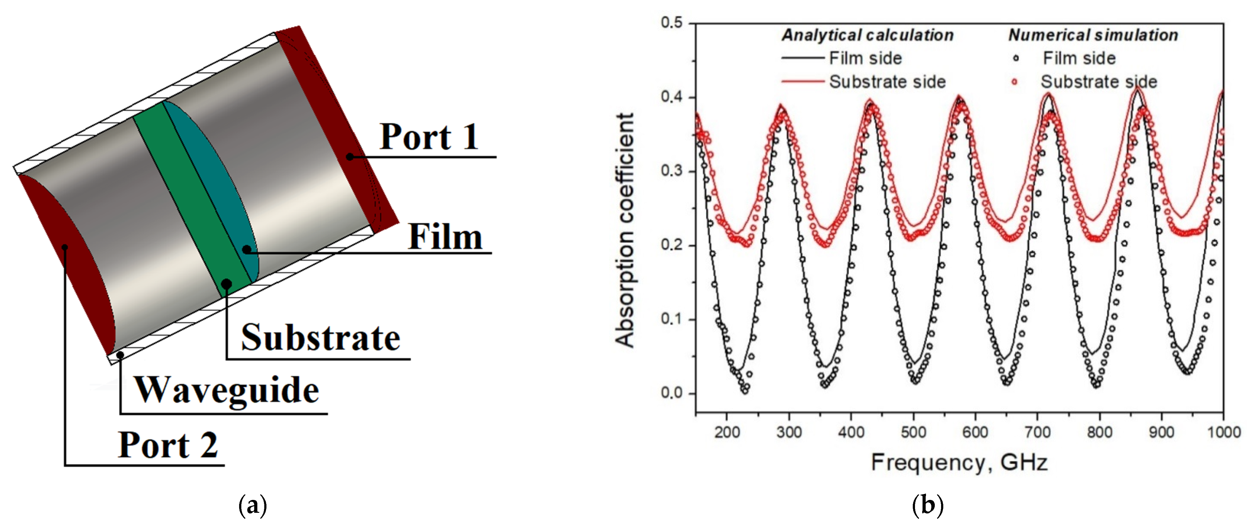
To model the absorption coefficient of thin film, CST Studio Suite was used. A schematic image of the project is presented in Figure 1a. Thin film on a substrate of the chosen material was placed inside the wave guiding structure (circular waveguide), and the two waveguide ports (377 Ω) were placed on both sides of the guiding structure to generate/receive the signal and determine S-parameters. The main feature of modelling such projects in CST is that when considering the film’s characteristics (skin depth and film thickness), the material of the metallic film must be determined as a “thin panel”, and the TLM module (in T-solver) is used for calculation. In the opposite case, the thin film will be treated as a “thick” metal surface, and regardless of the thickness (even zero), the transmittance coefficient will be zero. The absorption coefficient is calculated from S-parameters by the following formulas:
A 1 = 1 S 11 2 S 21 2   and   A 2 = 1 S 22 2 S 12 2
where A1 and A2 are the absorption coefficients in case of irradiation from the film side and the substrate side, respectively. The guiding structure is required because the waveguide port positioning should be used for calculation in this module. The results of modeling in CST with numerical calculation from [6] for film with a sheet resistance of 550 Ω/□ on sapphire substrate (340 μm thick) (Figure 1b) was compared to check the method. The modeling of films with different resistance values (Ω/□) is presented in Figure 2. The largest absorbance was observed for films with resistance of 188 Ω/□.
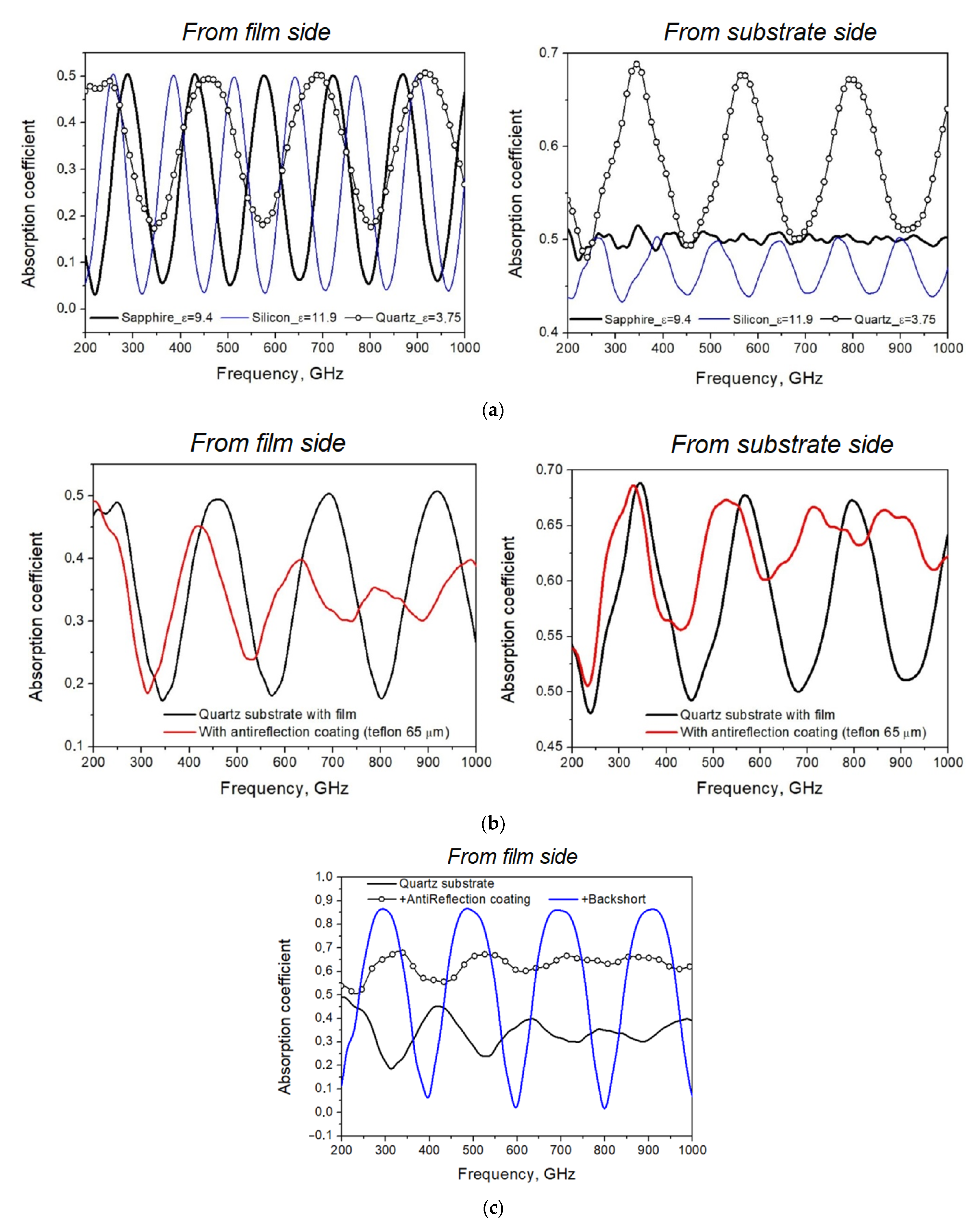
The bare dielectric substrate with refractive index n at both sides should have a reflection coefficient R = [(n − 1)/(n + 1)]2, so for silicon with n = 3.4, R = 0.3. Antireflection coating with electrical thickness of one-quarter wavelength and refractive index na = n0.5 can be used to decrease reflections in the relatively narrow band. The modeled absorption coefficients of film with resistance of 188 Ω/□ on different 340 μm substrates (sapphire, quartz, silicon) and on substrate with additional antireflective coating are presented in Figure 3.
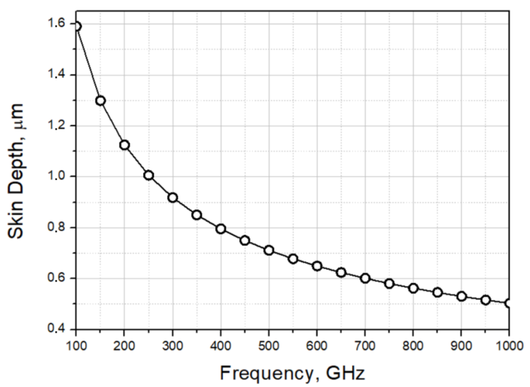
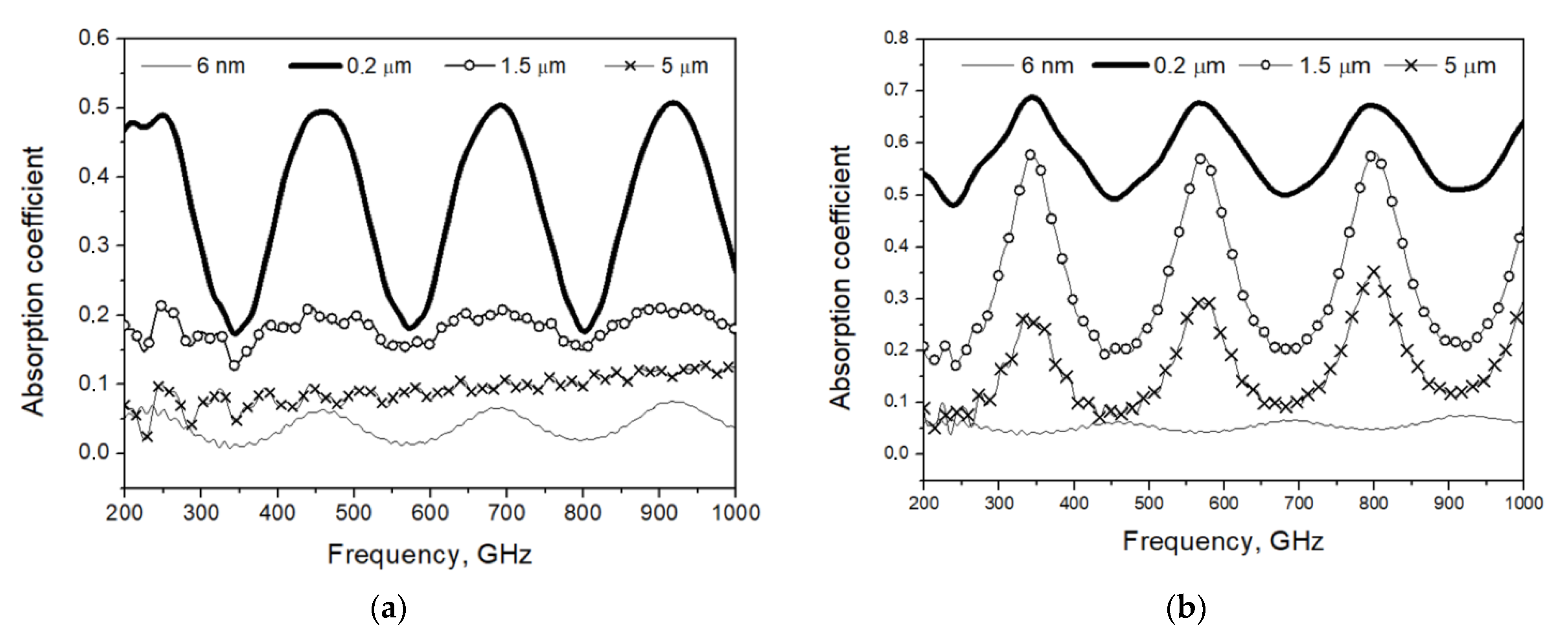
When using a substrate of finite thickness, the absorption spectrum becomes more complex because the periodic spectrum of the Fabry–Perot dielectric resonator is superimposed on the smooth dependence. This dependency is shown for the case of a resistive thin film with resistance per square of 30–300 Ω/□, which is too thin compared to the skin depth. So, for NiCr film with resistivity ρ = 10−6 Ωm, the resistance per square is 180 Ω/□ if the film thickness is 6 nm, but the skin depth of such film at f = 100 GHz is Δ = 503(ρ/f)0.5 = 1.5 μm. The calculated dependence of the skin depth on frequency is shown in Figure 4. This means that more than 90% of power is transmitted through the substrate (see Figure 5).
To increase the emissivity of a flat BB absorber, it is favorable to use relatively thick free-standing foil instead of an absorber comprising thin film on a dielectric substrate. For constantan with resistivity of 0.5 μΩ m at a signal frequency of 350 GHz, the skin depth is 0.6 μm, so 50 μm-thick foil is definitely opaque. In [
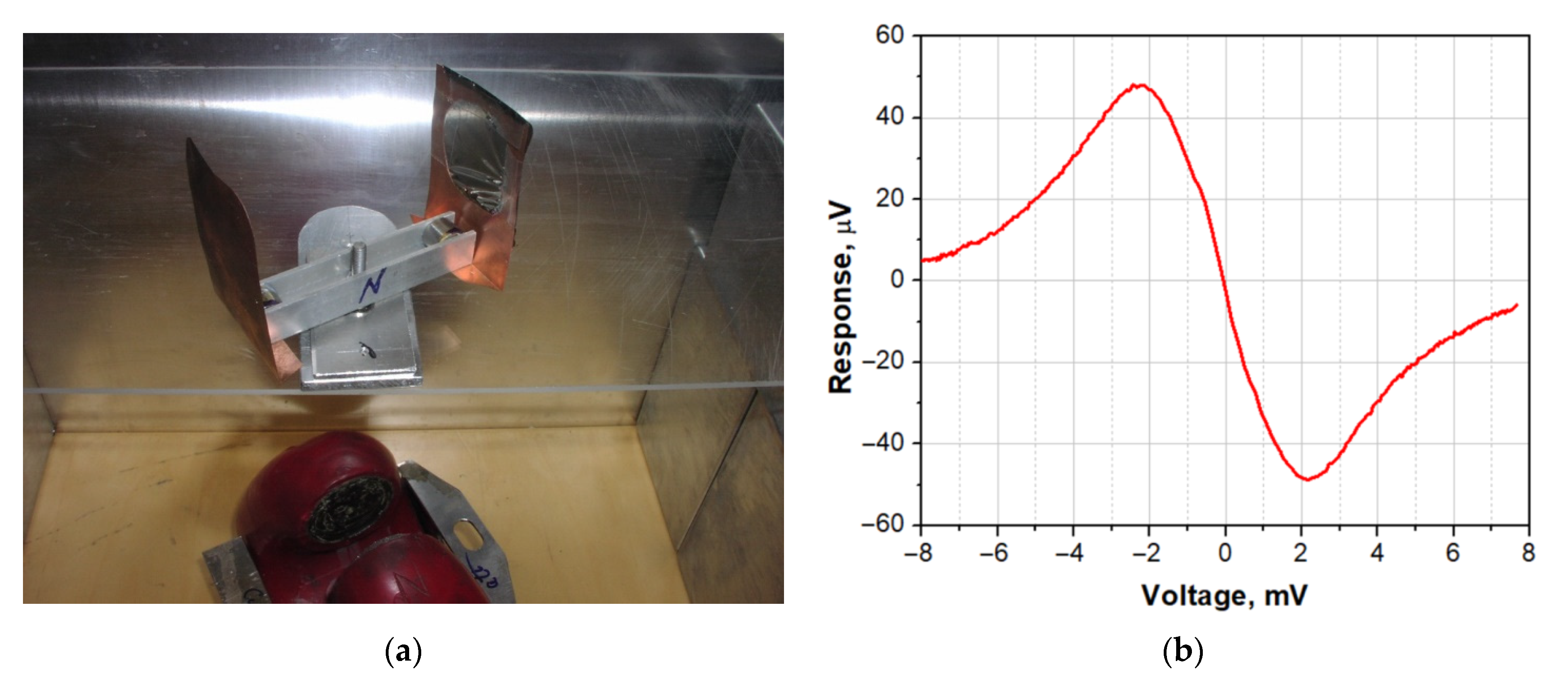
7], 50 μm constantan foil was mounted (glued by black thermally conductive STYCAST epoxy on copper foil to equalize the temperature) at a temperature stage of 0.4 K. On the reverse side, two resistors were glued to the copper carrier, one to measure the temperature and one for heating, and a miniature permanent magnet was mounted on this rotatable holder. The reflectance coefficient of the foil at a frequency of 350 GHz was measured by a BWO spectrometer/reflectometer; it was 0.7 ± 0.05, meaning that the blackness was k = 0.3 ± 0.05. Since such a source has high inertia, cold aperture switching was used for remote switching from cold to hot load by the external permanent magnet [8,9]. The whole assembly, which is fixed on an axle, can be rotated by the external magnet, and in this way, the hot or cold emitter appears in the aperture of the immersion lens. A demonstration of the room-temperature model of rotating cryogenic absorber and reflector is presented in Figure 6.
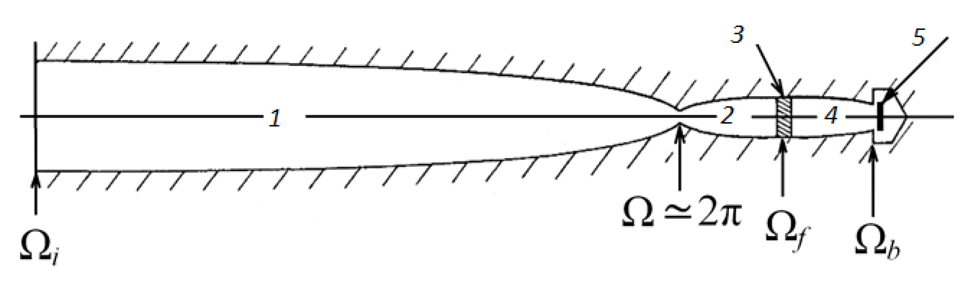
Using an integrating cavity in which the radiation is multiply reflected from the walls, accompanied by absorption in the semi-transparent film, can be a more effective method for increasing the absorption. Examples of devices with integrating cavities are shown in Figure 7, Figure 8 and Figure 9.
A series of samples on silicon substrate (24 × 5 × 0.5 mm) with different thicknesses of NiCr thin film was made to investigate the influence of film resistance and location on the efficiency of integrating cavity. The samples were mounted inside a spherical copper integrating cavity 33 mm in diameter with a 3.6 × 1.8 mm waveguide port, Figure 9b. The sample with thin film was glued at an angle of 10° in the middle of the sample holder. The reflectance coefficient was measured using a P2-69 reflection and transmission spectrometer in the frequency range of 52–80 GHz. At a frequency of 70 GHz for film with 100 Ω/□ resistance, the reflectance coefficient was −6.5 dB, indicating that the blackness was about 80%.
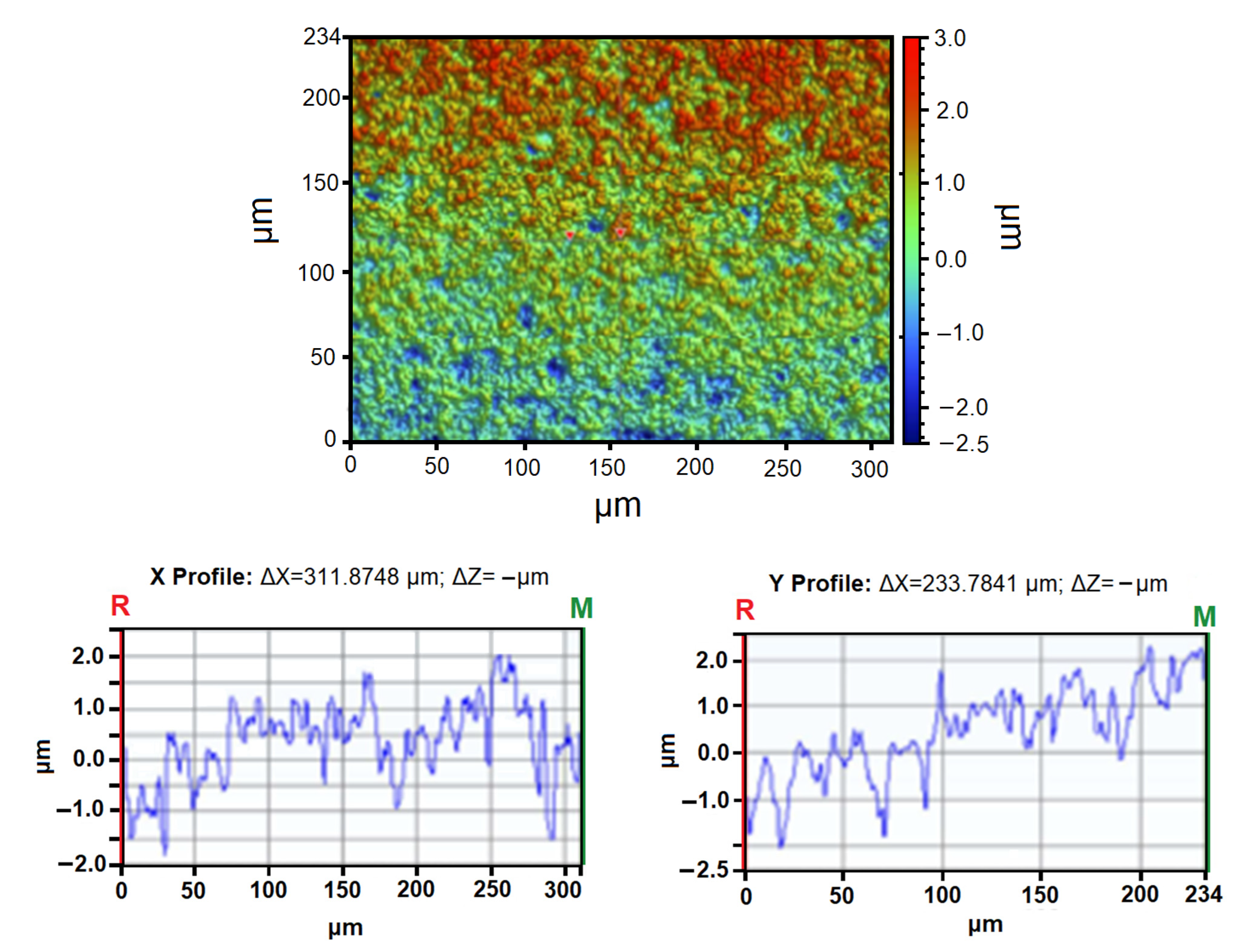
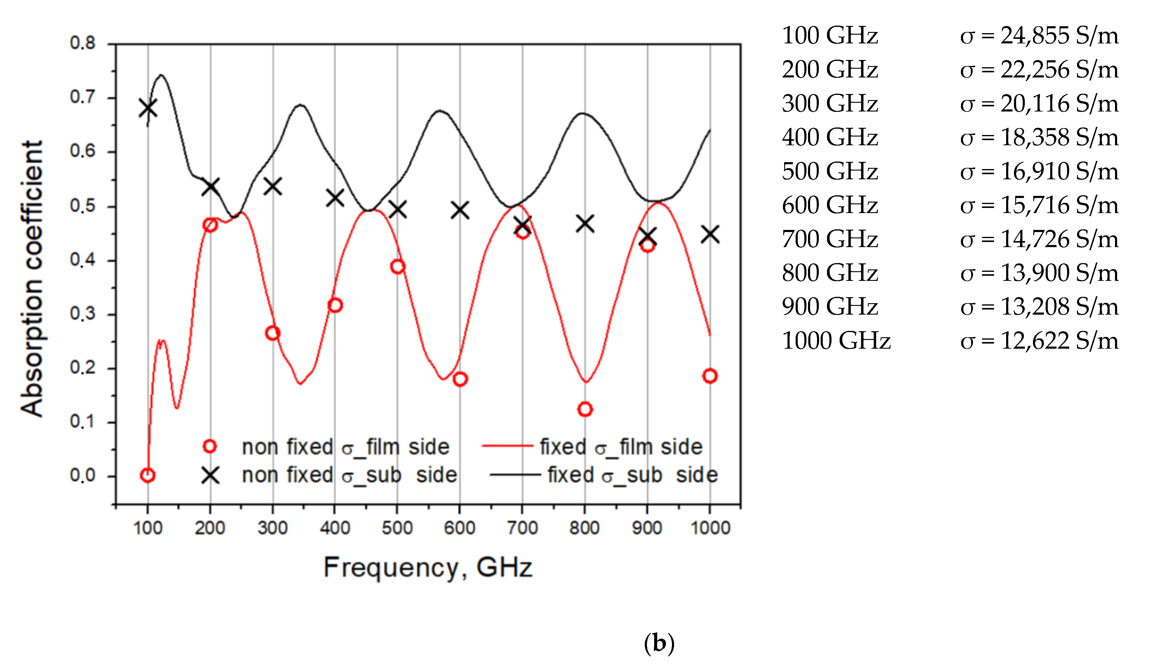
To increase scattering in the integrating cavity, the second type of sample was deposited on unpolished Si substrate 32 mm in diameter, which completely filled the middle of the cavity (a photo of the film surface and its profile are shown in 
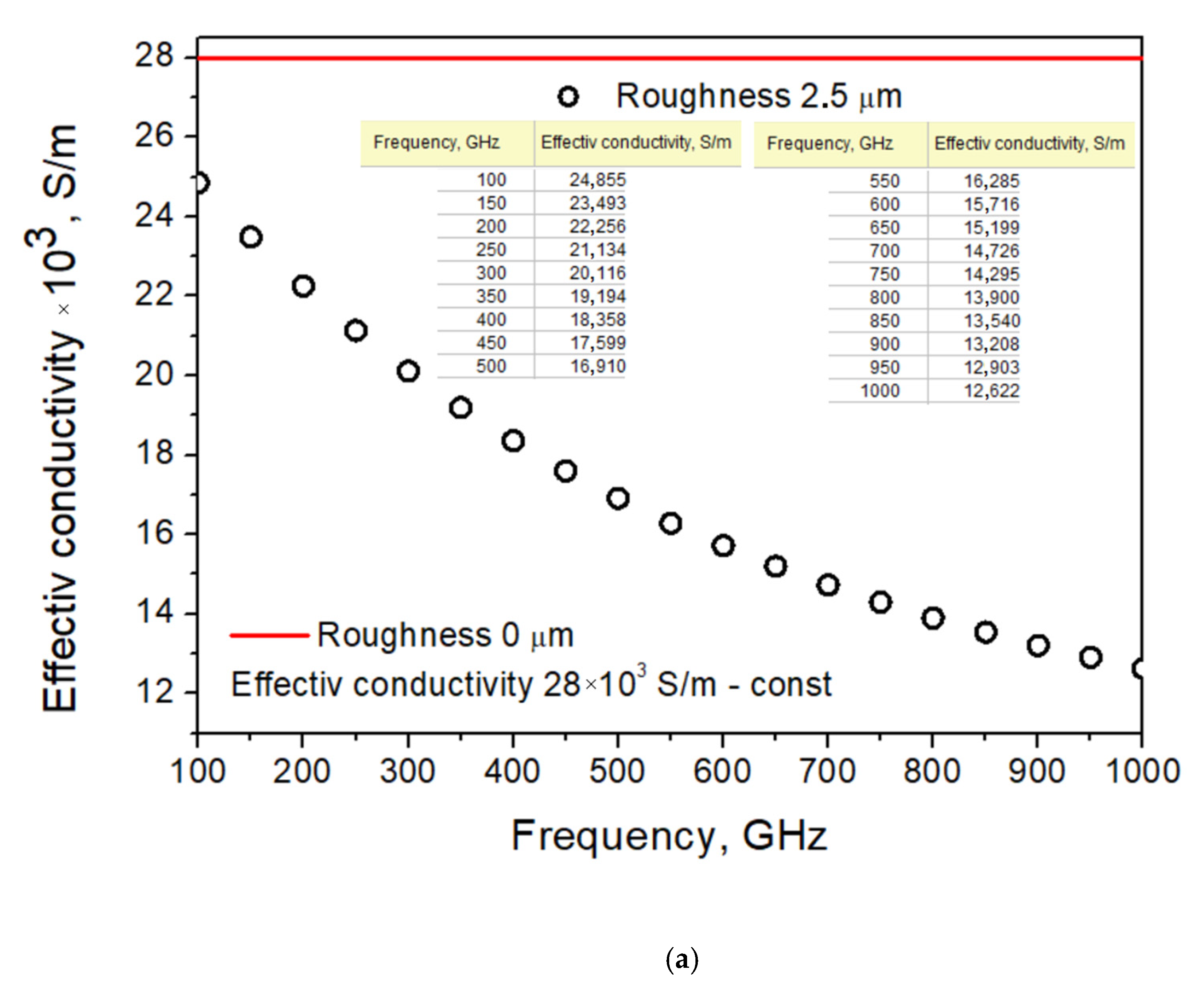
Figure 10). In this case, the blackness was more than 85%. The roughness of the surface was more than 1 μm, and resistance of NiCr thin film was 200 Ω/□, in contrast to the film on polished substrate (20 Ω/□), which was deposited by the same process as the film on unpolished substrate. The calculated dependence of effective conductivity on frequency for film roughness of 2.5 μm is presented in Figure 11a, and a comparison of absorption coefficients for perfect (with negligible roughness and fixed conductivity) and “real” substrate is presented in Figure 11b.

3. Fast Electrical Modulation of Radiation Temperature of Cryogenic Source

For measurements of SINIS detector optical response, a source of thermal blackbody radiation inside the cryostat was used in [12]. Thin nichrome film on a sapphire or silicon substrate was used as such source. At the sides of the NiCr film, gold contact pads were made to apply the heating current. The source was suspended on thin wires for thermal and electric insulation from the copper stage at a temperature of 0.5 K. The heating current was applied through the wires connected to the Au contact pads. DC current of a few mW provided heating up the BB source to 10–15 K. The temperature of the source was measured by an RuO2 thick-film resistor thermometer glued to the back side of the substrate. The radiation from the thermal source illuminated the detector through the mesh filters with 350 GHz central frequency and 70 GHz bandwidth. A hemispherical sapphire lens was used to focus the radiation onto the detector. The radiation power was calculated using Planck’s formula, taking into account the frequency band of filters. The relative value of power at different temperatures of the source depended only on the accuracy of temperature measurements.
To investigate the dynamic characteristics of the detector, a pulse of radiation with a sharp front was used. This pulse was formed by heating the blackbody source on a sapphire substrate. The heat capacity of sapphire is Csapphire = 29 × T3 nJ/K. The heat capacity of nichrome film and gold contacts with thickness less than 1 μm is low compared to the heat capacity of sapphire substrate. Applying an electrical pulse with energy of 1 μJ heats the source to ~3.5 K, and after that, the source holds this temperature up to a hundred milliseconds. The test measurements with pulse heating of sources on silicon substrates show that the response time of the RuO2 thermometer is about 200 microseconds. For estimation of the temperature and power of the source on sapphire substrate, depending on the applied power under DC current, we compared the detector response with the measured response of the BB source on silicon substrate.
For estimation of the radiation power variation over time, we modeled the process of thermal dynamics in the source before and after heating by current pulse. A two-dimensional thermal conductivity equation was solved by the finite element method. We used the value of 0.253 T mJ/g K [13] for a specific heat capacity of NiCr. The thermal conductivity of sapphire in such calculations was taken of 3.5 × T3 W/(m K).
The temperature difference between the nichrome film and the sapphire substrate at T = 4 K was less than 0.2 K and changed with temperature as T−3. Such estimation used the Kapitza resistance at the indium–sapphire interface [14], which is larger compared to the nichrome–sapphire clean interface. Based on this, the Kapitsa resistance was not taken into account in the calculation. Examples of such calculations are shown in
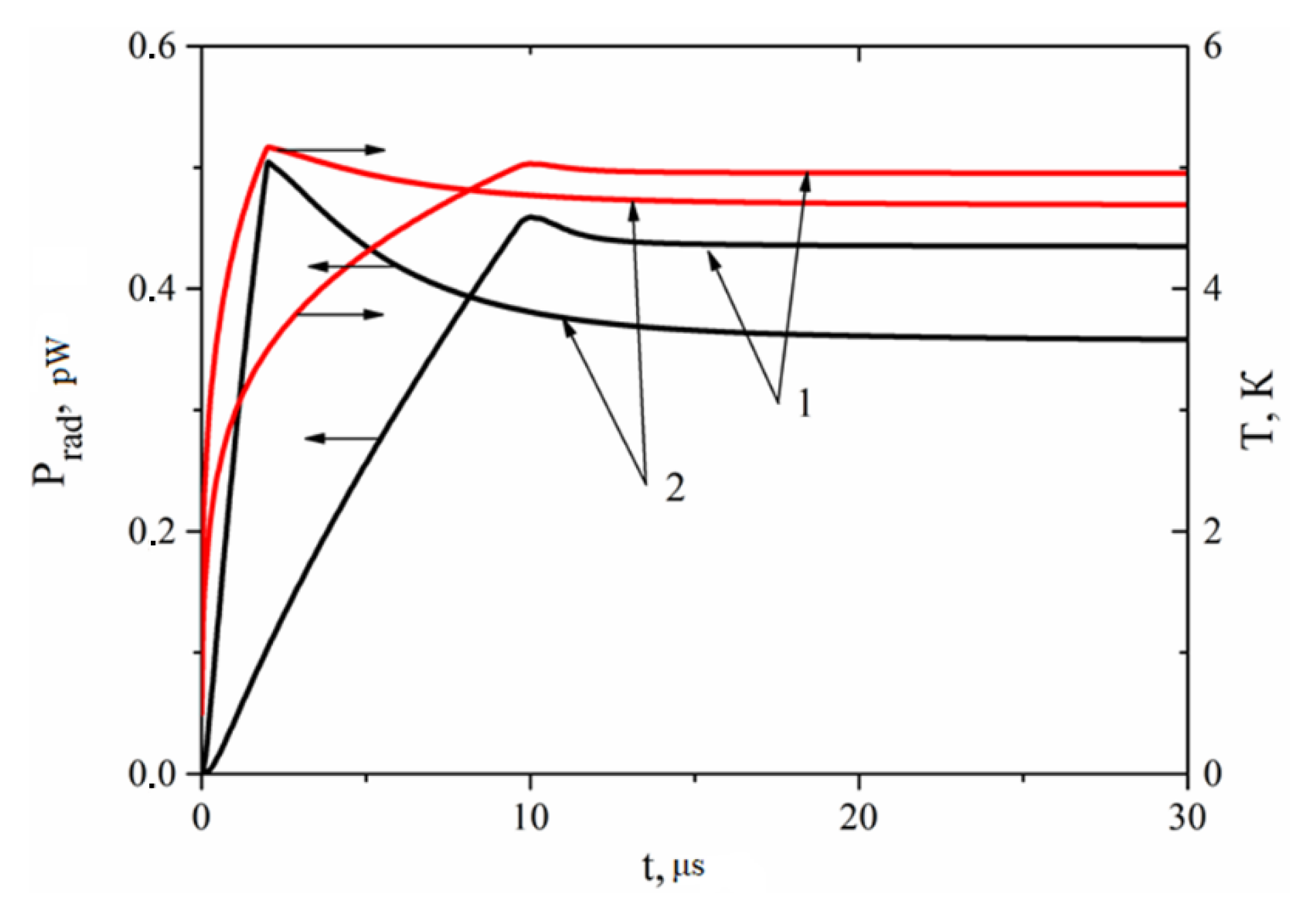
 Figure 12.
At the end of the pulse, the radiation power approaches maximum and then exponentially decreases with a time constant of ~4 μs. This decay corresponds to heat redistribution from the heating area to the area under the 2–3 mm-wide gold contact pads.
The BB source was heated by current pulses of 5–90 V from the pulse generator. The output signal of the preamplifier was applied to one of the inputs of the 2-channel oscilloscope Tektronix TDS 1012B operating in waiting mode. The heating pulses were fed through 1:10 or 1:100 dividers to the second input of the oscilloscope. The amplitude of these pulses had to be reduced because a noticeable parasitic interaction was found between the oscilloscope channels, affecting the detector; the electrical signal caused additional heating of the absorber. In order to reduce the electrical pulse interference penetrating into the registration system and bypass the detector, measurements were made in the bias reversal mode of the detector. The response to radiation was obtained by subtracting the signals at positive and negative bias voltages. Adding them together brings the level of interference. The results were averaged during 1024 cycles. The period between cycles was up to 5 s depending on the level of source heat, in order to ensure cooling of the source between heating pulses.
We estimated the time constant of preamplifier τamp and twisted pair τRC. The measured capacitance in the feed line is 
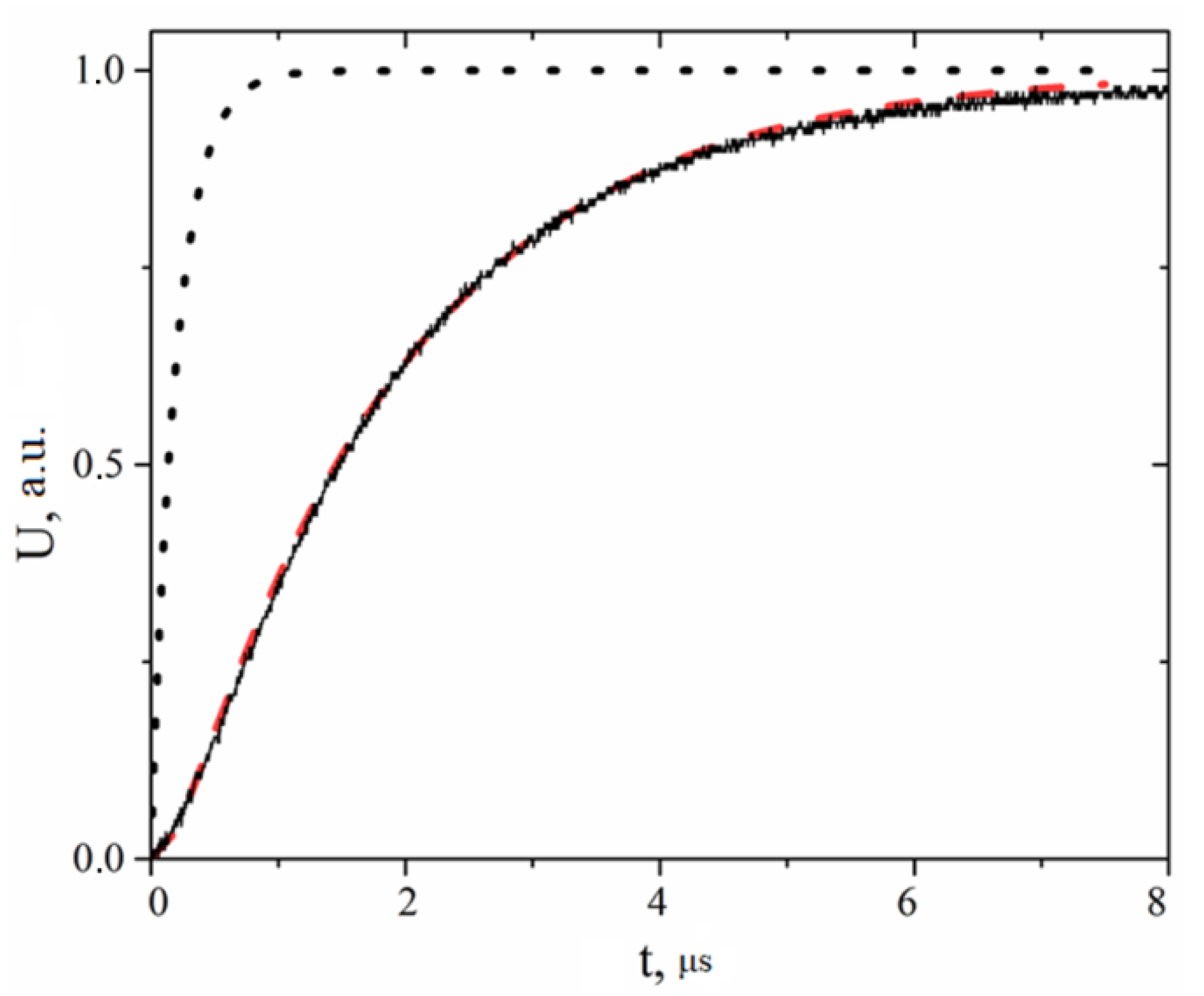
C = 80–100 pF, and the dynamic resistance of the detector at the working point is in the range from tens to hundreds of kΩ, so the time constant of such RC circuit is up to 10 μs. Some measurements of the time constant of the whole system were carried out at room temperature using an optocoupler pair instead of a detector. A pulse from the heater generator was applied to the LED of the pair. The photodiode of the optocoupler was connected in series with a resistor R (from 1 to 100 kΩ) to the input of the transmission line. A simulated output signal with R = 14 kΩ is shown in Figure 13. It can be described by an exponent, and for the case shown in the figure, the time constant is 1.8 μs.
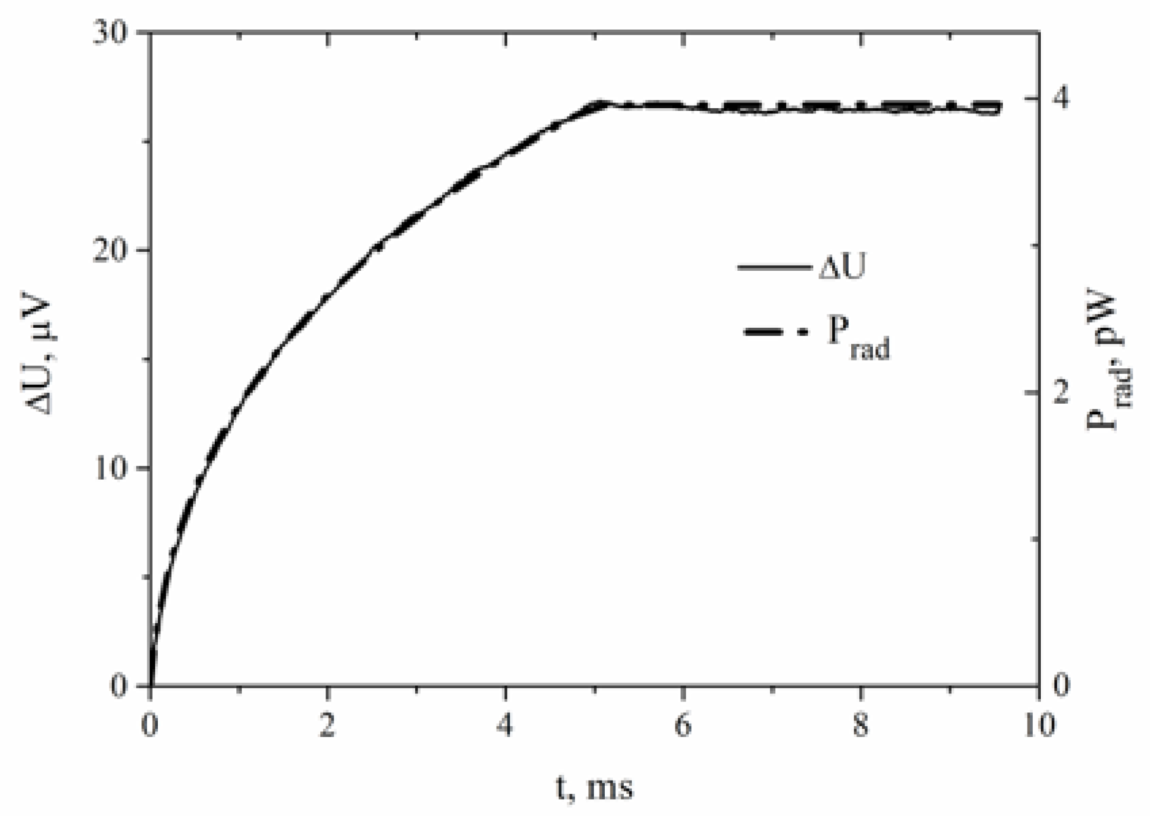
The performance of the BB source is tested by the detector response when millisecond heating pulses of moderate voltage are applied (see Figure 14). The temperature of the source is calculated by its thermal capacity and applied pulse energy. The power of radiation is calculated from the equation for a single mode SINIS detector. The detector response is proportional to the calculated radiation power, which confirms the correctness of the described procedure for estimation of the radiation power. The radiation power after applying pulses with front duration of 1 ms was estimated in the same way.
The measurement results of a SINIS detector response time presented in Figure 15. Unlike the previous cases, for this measurement, the voltage pulses had higher amplitude but shorter duration. As shown in Figure 15, the pulse duration and amplitude were chosen so that the total heat power of the pulses would be close in both cases. The main feature of the presented data is the noticeable difference between the detector response and the output signal rise time of 1.8 μs. Agreement with the experiment is achieved if we take into account the proper response time of the detector τdet. For 10 μs heating pulses, tbol = 1.8 ± 0.5 μs. At such values, the standard deviation of δU in the experiment is minimal at 0.19 μV, which practically coincides with δU in the constant signal level region and is less than the value of 0.33 μV without taking into account the detector’s own time constant.
For 2 μs pulses using the same procedure of operating the detector time, the response is tdet = 0.8 ± 0.3 μs (Figure 15b). Apparently, this discrepancy is due to a greater overheating of the emitting nichrome film relative to the sapphire substrate than was calculated, which led to a faster increase in the response at the beginning of the process. This is clearly seen in Figure 16, which shows the results for heating pulses with a duration of 0.4 μs and an amplitude of 90 V. In this case, the dependence ΔU(t) shows a maximum at t = ~3 μs, which is much later than the end of the heating pulse. Obviously, at this time, the intensity of radiation corresponds to the actual response value and is 1.3–1.4 times greater than the asymptotic value at t = ~7 μs. According to the simulation, this difference may only be 5–6%. It is not possible to achieve agreement with the experiment by changing the parameters of the model in a wide range. The overheating of the film may be due to the poor thermal conductivity of the surface layer of sapphire. According to the results shown in Figure 15, with heating pulses of 20 V and 10 μs, the overheating of the film is too small, and the estimation tdet = 1.8 ± 0.5 μs is close to the true value of the detector’s response time.

4. Discussion

This paper presents an analysis of the performance of a simple blackbody source comprising a thin metal film on a dielectric substrate, demonstrating that emissivity even in the best case is in the range of 0.3–0.5, which leads to overestimation of incident power. The practical solution to improve the accuracy of the BB radiation source is to place it in the integrating cavity, which can be spherical with waveguide output or back-to-back horn for a quasioptical beamguide. Fast electric modulation of radiation temperature can be managed by deposition of such absorber/heater on sapphire substrate with a proper heat sink that provides modulation frequency up to 1 kHz.

5. Conclusions

The calculations and measurements presented in this paper demonstrate that using a simple blackbody radiation source in the form of a thin film on a silicon or sapphire substrate can lead to overestimation of the level of received radiation. The experimental values of emissivity were in the range of 0.2–0.5. A thin metal film with square resistance of 30–300 Ω was too thin relative to the skin depth. This means that more than 90% of the power passes through the film and is reflected from two boundaries of the vacuum–substrate and substrate–vacuum interface. A practical method of increasing absorption (emission) could be to use an integrating cavity in which there are multiple reflections of radiation from the conducting walls, accompanied by multiple absorption in semitransparent film. Such a blackbody source could be used for internal calibration of superconducting receivers. Compared with a massive corner reflector, the power of such a source could be modulated with a frequency up to 1 kHz, which makes it possible to use lock-in detection and significantly increase the signal-to-noise ratio and accuracy of measurement at the ultimate low-signal level.

Author Contributions

Conceptualization, M.T. and V.E.; methodology, M.T.; software, A.G.; validation, M.T., A.C. and M.S.; resources, M.T.; data curation, V.E.; writing—original draft preparation, M.T.; writing—review and editing, A.G.; visualization, A.G.; supervision, V.E.; project administration, M.T.; funding acquisition, M.T. All authors have read and agreed to the published version of the manuscript.

Funding

Numerical calculations and modeling were supported by a grant from the Russian Science Foundation 21-42-04421. The manufacture of blackbody samples with NiCr film was carried out as part of the state assignment of the IRE RAS № FFWZ 2022-0005 using the equipment of USU “Cryointegral”, which is supported by a grant from the Ministry of Science and Higher Education of the Russian Federation, agreement No. 075-15-2021-667. Low-temperature experiment was carried out within state assignment of the IAP RAS (No. 0030-2021-0005).

Institutional Review Board Statement

Not applicable.

Informed Consent Statement

Not applicable.

Data Availability Statement

Not applicable.

Acknowledgments

The authors acknowledge valuable advice from S. Lemzyakov, G. Bogomolov and V. Zavyalov.

Conflicts of Interest

The authors declare no conflict of interest.

References

  1. Persky, M.J. Review of black surfaces for space-borne. Rev. Sci. Instrum. 1999, 70, 2193–2217. [Google Scholar] [CrossRef]
  2. Surrey Nanosystems. Vantablack Coating Technology. Available online: https://www.surreynanosystems.com (accessed on 31 May 2022).
  3. Hargravea, P.; Wasketta, T.; Limb, T.; Swinyardb, B. Performance of flight-model on-board calibration sources on Herschel-SPIRE. In Proceedings of the SPIE Astronomical Telescopes + Instrumentation, Orlando, FL, USA, 24–31 May 2006; Volume 6275. [Google Scholar] [CrossRef]
  4. Pisano, G.; Hargrave, P.; Griffin, M.; Collins, P.; Beeman, J.; Hermoso, R. Thermal illuminators for far-infrared and submillimeter astronomical instruments. Appl. Opt. 2005, 44, 3208–3217. [Google Scholar] [CrossRef] [PubMed]
  5. Parmar, N.; Sinha, A.; Pathak, S.K.; Kshatriya, A.J. Design and simulation of high temperature black body source for calibration of Michelson interferometer ECE diagnostic. Fusion Eng. Des. 2021, 172, 112752. [Google Scholar] [CrossRef]
  6. Lemzyakov, S.A. Interaction of Submillimeter Wave Radiation with SINIS Structures. Ph.D. Thesis, P. Kapitza Institute for Physical Problems, Moscow, Russia, 2021. [Google Scholar]
  7. Tarasov, M.; Kuzmin, L.; Edelman, V.; Kaurova, N.; Fominsky, M.; Ermakov, A. Optical response of a cold-electron bolometer array. JETP Lett. 2010, 92, 416–420. [Google Scholar] [CrossRef]
  8. Tarasov, M.A.; Kuzmin, L.S.; Kaurova, N.S.; Otto, E.A.; Yassin, G.; de Bernardis, P. Cold-electron bolometer array integrated with a 350 GHz cross-slot antenna. In Proceedings of the 21 International Symposium on Space Terahertz Technology, Oxford, UK, 23–25 March 2010; pp. 256–261. [Google Scholar]
  9. Tarasov, M.; Kuzmin, L.; Edelman, V.; Mahashabde, S.; de Bernardis, P. Optical response of a cold-electron bolometer array integrated in a 345 GHz cross-slot antenna. IEEE Trans. Appl. Supercond. 2011, 21, 3635–3639. [Google Scholar] [CrossRef]
  10. Nishioka, N.S.; Richards, P.L.; Woody, D.P. Composite bolometers for submillimeter wavelengths. Appl. Opt. 1978, 17, 1562–1567. [Google Scholar] [CrossRef] [PubMed]
  11. Tarasov, M.A.; Chekushkin, A.M.; Yusupov, R.A.; Gunbina, A.A.; Edelman, V.S. Matching of radiation with array of planar antennas with SINIS bolometers in an integrating cavity. J. Commun. Technol. Electron. 2020, 65, 60–68. [Google Scholar] [CrossRef]
  12. Lemzyakov, S.A.; Tarasov, M.A.; Edelman, V.S. Investigation of the Speed of a SINIS Bolometer at a Frequency of 350 GHz. J. Exp. Theor. Phys. 2018, 126, 825–832. [Google Scholar] [CrossRef]
  13. Lemzyakov, S.A.; Edelman, V.S. The use of RuO2 resistors as broadband low-temperature radiation sensors. Instrum. Exp. Tech. 2016, 59, 621–626. [Google Scholar] [CrossRef]
  14. Tomaru, T.; Suzuki, T.; Uchiyama, T.; Yamamoto, A.; Shintomi, T.; Taylor, C.T.; Yamamoto, K.; Miyoki, S.; Ohashi, M.; Kuroda, K. Maximum heat transfer along a sapphire suspension fiber for a cryogenic interferometric gravitational wave detector. Phys. Lett. A 2002, 301, 215–219. [Google Scholar] [CrossRef]
Figure 1. Methods of modeling absorption coefficient: (a) schematic image of modeled project (cross-section); (b) results of modeling for film with resistance of 550 Ω/□ on 340 μm sapphire substrate and comparison with calculation of same film from [6] (Reprinted with permission. Copyright 2021 Lemzyakov, S.A.).
Applsci 12 07349 g001
Figure 2. Modeled absorption coefficient for films with different resistance values (Ω/□): (a) irradiation from film side; (b) irradiation from substrate side.
Applsci 12 07349 g002
Figure 3. Modeled absorption coefficient of film with resistance of 188 Ω/□ on different substrates: (a) sapphire, silicon and quartz 340 μm substrates, irradiation of film side (left) and substrate side (right); (b) quartz 340 μm substrate with antireflection coating made of 65 μm-thick Teflon, irradiation from film side (left) and substrate side (right); (c) comparison of results of modeling absorption coefficient of thin film on quartz substrate without and with antireflection coating and with additional backshort behind antireflection coating.
Applsci 12 07349 g003
Figure 4. Dependence of skin depth on frequency for film with resistance of 180 Ω/□.
Applsci 12 07349 g004
Figure 5. Calculated absorption coefficient of films with different thickness. Irradiation from (a) film side and (b) substrate side.
Applsci 12 07349 g005
Figure 6. (a) Room-temperature demonstration model of rotating cryogenic absorber and reflector and (b) measured voltage response of SINIS detector to switching of aperture from reflector to thin film 10 dB absorber made on Kapton.
Applsci 12 07349 g006
Figure 7. Construction of integrating cavity (reprinted with permission from ref. [10], Figure 4, Copyright 1978 The Optical Society): (1) Winston concentrator determining throughput AΩ; (2) second concentrator; (3) bandpass filter; (4) third cone; (5) directly irradiating bolometer in third cavity.
Applsci 12 07349 g007
Figure 8. (a) Schematic view of matching horn device (1) with integrating cavity (2) of Planck space observatory surveyor satellite and (3) incoming radiation, and (b) our construction of back-to-back horn (4) and flat backshort (7) with array of annular planar antennas (6) with SINIS detectors on silicon substrate (5) (Reprinted with permission from Ref. [11]. Copyright 2020 Pleiades Publishing, Ltd.).
Applsci 12 07349 g008
Figure 9. (a) Integrating cavity with NiCr film on sapphire substrate at 2.8 K stage in cryostat with the sample (left) at 280 mK stage; (b) photo of spherical integrating cavity for measurements with P2-69 SWR meter.
Applsci 12 07349 g009
Figure 10. Images of rough silicon substrate with deposited NiCr 280 nm film.
Applsci 12 07349 g010
Figure 11. Calculated dependence of film characteristics on surface roughness: (a) dependence of effective conductivity on frequency for film with roughness of 2.5 μm; (b) absorbance coefficient of thin film at different frequencies depending on value of effective conductivity.
Applsci 12 07349 g011aApplsci 12 07349 g011b
Figure 12. Calculation of changing temperature (T, red curves) and radiation power (Prad, black curves) at applied pulse of 10 μs (1) and 2 μs (2) and 20 and 40 V starting at t = 0. Pulse power applied to nichrome film is 0.19 and 0.75 W/cm2. Graph from [12] with permission, Copyright 2018 Pleiades Publishing, Ltd.
Applsci 12 07349 g012
Figure 13. Output signal (solid line) dependence on time for voltage applied to optocoupler (dot) through 14 kΩ resistor. Dashed line indicates exponent with τ = 1.8 μs, see also [12] (Reprinted with permission, Copyright 2018 Pleiades Publishing, Ltd.).
Applsci 12 07349 g013
Figure 14. Solid line indicates detector response to source radiation when 7 V pulse was applied for 5 ms. Dashed line indicates calculated radiation power, Reprinted with permission from Ref. [12], Copyright 2018 Pleiades Publishing, Ltd.
Applsci 12 07349 g014
Figure 15. Detector response to pulses applied to BB source: (a) Urad = 26 V, 10 μs; (b) Urad = 40 V 2 μs. Curve 1: measured detector response. Curve 2: calculated response taking into account dependencies of Prad(t) and registration time τ = 1.8 μs with τdet = 0. Curve 3: calculation taking into account detector response time τdet = 1.8 μs (a) and τdet = 0.8 μs (b), see also [12] (Reprinted with permission, Copyright 2018 Pleiades Publishing, Ltd.).
Applsci 12 07349 g015
Figure 16. Detector response for pulse amplitude Urad = 90 V, duration 0.4 μs, applied to BB radiator.
Applsci 12 07349 g016
Publisher’s Note: MDPI stays neutral with regard to jurisdictional claims in published maps and institutional affiliations.

