Article

Factor Design for the Oxide Etching Process to Reduce Edge Particle Contamination in Capacitively Coupled Plasma Etching Equipment

Department of Mechanical Engineering, National Yang Ming Chiao Tung University, Hsinchu City 30010, Taiwan
*
Authors to whom correspondence should be addressed.
Appl. Sci. 2022, 12(11), 5684; https://doi.org/10.3390/app12115684
Submission received: 28 April 2022 / Revised: 26 May 2022 / Accepted: 27 May 2022 / Published: 3 June 2022
(This article belongs to the Topic Advanced Systems Engineering: Theory and Applications)

Abstract

:
During the oxide layer etching process, particles in capacitively coupled plasma etching equipment adhere to the wafer edge and cause defects that reduce the yield from semiconductor wafers. To reduce edge particle contamination in plasma etching equipment, we propose changes in the voltage and temperature of the electrostatic chuck, plasma discharge sequence, gas flow, and pressure parameters during the etching process. The proposed edge particle reduction method was developed by analyzing particle maps after wafer etching. Edge particle adherence in plasma etching equipment can be reduced by decreasing the voltage and temperature changes of the electrostatic chuck and generating a plasma sheath with a continuous discharge sequence of radio-frequency plasma. The gas pressure and flow rate also affect the number of wafer edge particles. Experimental results were used to optimize the equipment parameters to reduce edge particle contamination and improve edge wafer defects after dry etching.

1. Introduction

Plasma etching is a key processing technology that is widely used in the semiconductor industry. Particle contamination in the plasma etching process can cause defects on the wafer surface [1,2,3,4,5,6,7,8]. In the plasma etching process, the particles per wafer pass test is periodically performed to reduce chamber contamination. If the number of particles exceeds a predefined threshold, the chamber must be wet-cleaned [9]. In situ particle monitors have been used in the semiconductor industry for many years to monitor chamber conditions before and after preventative maintenance [10]. Controlling particle defects is key for achieving the high-yield requirements of semiconductor manufacturing [11]. The generation and behavior of particles in etching systems were demonstrated to be related to the operating characteristics of the etching equipment [12] and can be monitored using the laser scattering method [13]. Particles may be generated from chamber walls; consumables, or electrostatic chucks in the chamber [14,15,16,17]; or from related process recipes, including process characteristics or imperfect process design [18,19]. Particle contamination persists [20] despite regular chamber cleaning and maintenance activities, including circulating the chamber, wiping the electrostatic chuck (ESC), and replacing the consumable parts of the chamber. A particle contamination analysis and ESC inspection revealed that the deposition of by-products generated during the etching process during the ESC discharge step is the root cause of particle generation. Therefore, the deposition of suspended particles on the ESC during discharge steps is the main source of particle contamination, and the modification of discharge steps can reduce the rate of defect formation caused by suspended particles [21]. Gas viscous forces or electrostatic forces generated during the etching process, the shock wave generated by the applied voltage, and radio-frequency (RF) discharge cause particles comprising silicon, carbon, oxygen, fluorine, or aluminum to be suspended in the wafer or stick on wafer [22] (Figure 1). This deposition frequently occurs during the process steps or when chamber by-products are insufficiently cleaned [23]. Particle maps generated after the oxide layer etching process reveal that the particle distribution on the edge of the wafer is a major problem [24,25]. We analyzed a mechanism that may generate edge particles during the wafer etching process and optimized the process conditions with an experiment to reduce edge particle deposition on the wafer and improve edge defects in the plasma dry etching process.
The rest of this paper is organized as follows. Section 2 introduces the basic parameters of plasma and the theory of dust in the plasma sheath. Section 3 describes the main experimental equipment and methods. Section 4 describes the effects of different process parameters on the wafer particles in the dry etching equipment. Finally, Section 5 presents the conclusions of this study.

2. Basic Principles of Particle Transport in Plasmas

This section describes the theory used to design our method. The proposed approach involves optimizing RF plasma parameters on the basis of plasma sheath theory. The effect of the force acting on the charged dust particles in a suspended plasma sheath is described.

2.1. RF Plasma

RF plasma is one of the types of application technologies commonly used in semiconductor manufacturing. RF plasma is generated by applying a high frequency (MHz) sinusoidal voltage, which creates an electric field in which charge carriers are accelerated and participate in the ionization of the gas. Because this study was performed using capacitively coupled plasma (CCP), the plasma is created by applying an electric field between two electrodes. In an RF CCP discharge, while the plasma is nearly equipotential, it forms a sheath with the transition region between adjacent dielectrics (including vacuum chamber walls, electrodes, substrates, etc.). This sheath is characterized by large potential changes and low electron density. There is a strong electrostatic field in the sheath; the direction is from the plasma area to the electrode surface. The electric field of the sheath can confine electrons to a certain extent, accelerating positive ions to attack the electrode plates. Another critical part of an RF plasma source is the matching network. The matching network allows an impedance of 50 Ω between the generator and the load impedance (plasma) and creates resonance in the power transfer from the generator to the plasma to reduce the occurrence of power losses.

2.2. Debye Length

In this section, we introduce the key parameters used to define plasma. Not all particles in plasma are ions; many particles are neutral. The characteristic distance of electrostatic interactions in plasma is called the Debye length. The Debye length for electrons and ions ( λ D e , i ) is defined as follows:
                λ D e , i = ε 0 k T e , i e 2 n
where ε 0 is the dielectric constant in vacuum, k is the Boltzmann constant, T e , i is the electron and ion temperature, e is the electron charge, and n is the plasma density. In a typical low-pressure capacitively coupled RF plasma, the electron temperature is T e ≈ 3 eV, the ion temperature is T i ≈ 0.03 eV, and the plasma density is n = 5 × 10¹⁵ m−3.

2.3. Dust in the Plasma Sheath

In capacitively coupled RF plasma, negatively charged particles are affected by electrostatic forces. Gravity also affects plasma particles. In the plasma sheath, ions accelerate toward the electrode because of the electrostatic field [26]. These moving ions exert a force called ion resistance on the dust particles. Plasma typically contains gas flow that produces neutral resistance. Even without gas flow, neutral resistance still acts on the moving particles in plasma.

2.3.1. Gravity

Every dust particle in plasma is subject to gravitational force. For spherical particles, this force is defined as follows:
F g = m p g = 4 3 π r p 3 ρ g
where m p is the dust particle mass, g is the gravitational acceleration, ρ is the particle density, and r P is the particle radius. The gravitational force acts downward on the particles and has a cubic dependence on the particle radius.

2.3.2. Electric Force

The dust particles in the plasma are negatively charged. For the electric force acting on such particles, which causes the trapping of the dust particles in the plasma, the expression is
F E = Q P E
where Q P is the dust particle charge, and E is the applied electric field. The electric force is directed inward (i.e., toward the plasma glow) and traps dust particles within the plasma. The electric field mainly refers to radio frequency plasma and electrostatic field, including radio frequency power and ESC voltage output.

2.3.3. Gas Viscous Force

Gas viscous force causes particles to suspend when they continuously collide against gas molecules. Resuspended particles are accelerated in the direction in which the gas is flowing. The gas viscous force is expressed by the following equation
  f n = ρ · υ n · m n · υ R · π r p 2
where υ n is the thermal velocity of a gas molecule, m n is the mass of the gas molecule, υ R is the relative velocity between a particle and the gas, and r p   is the radius of the particle. Gas-induced particle resuspension is therefore not only due to shock waves, but also to gas viscous forces [18].

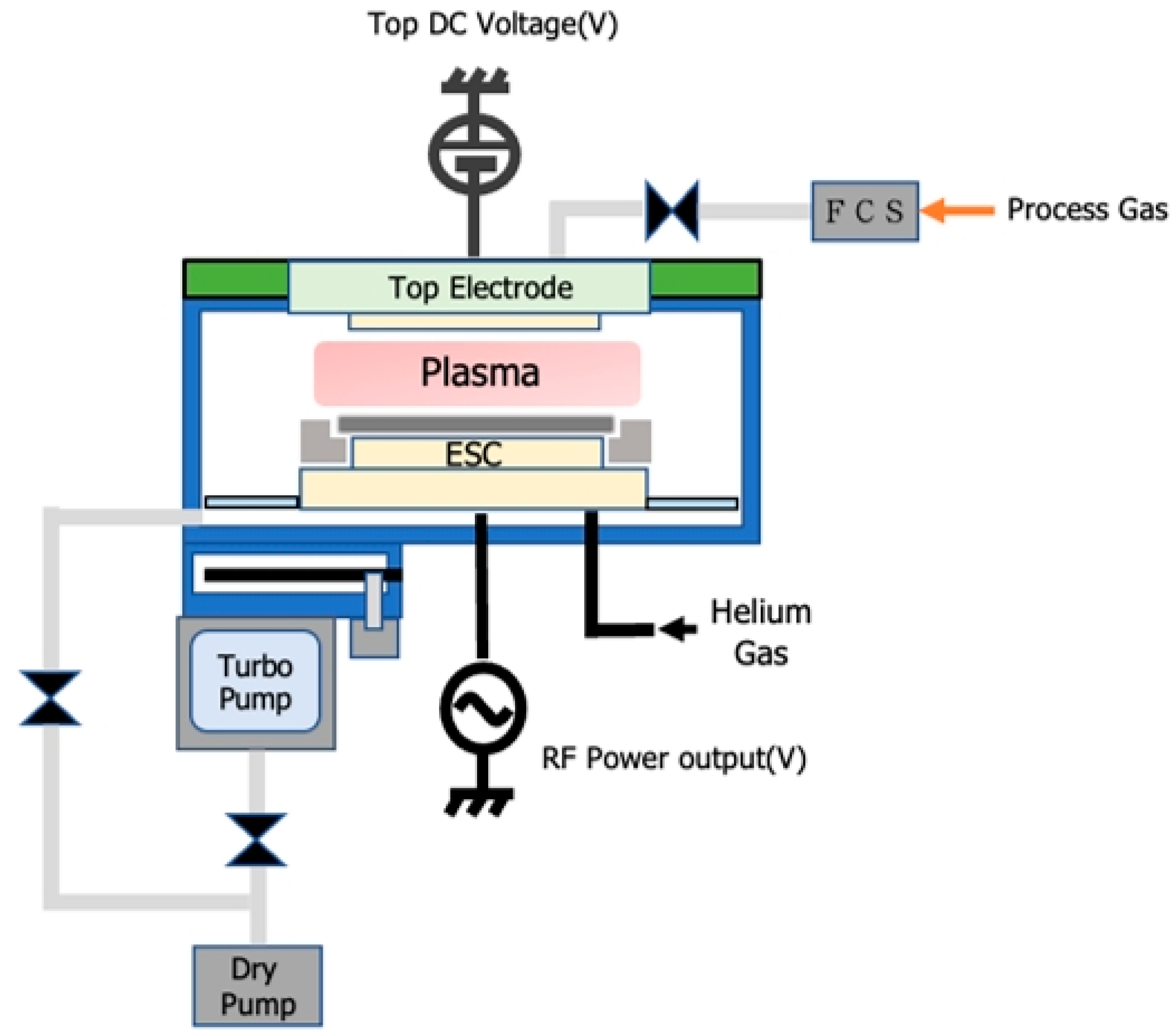
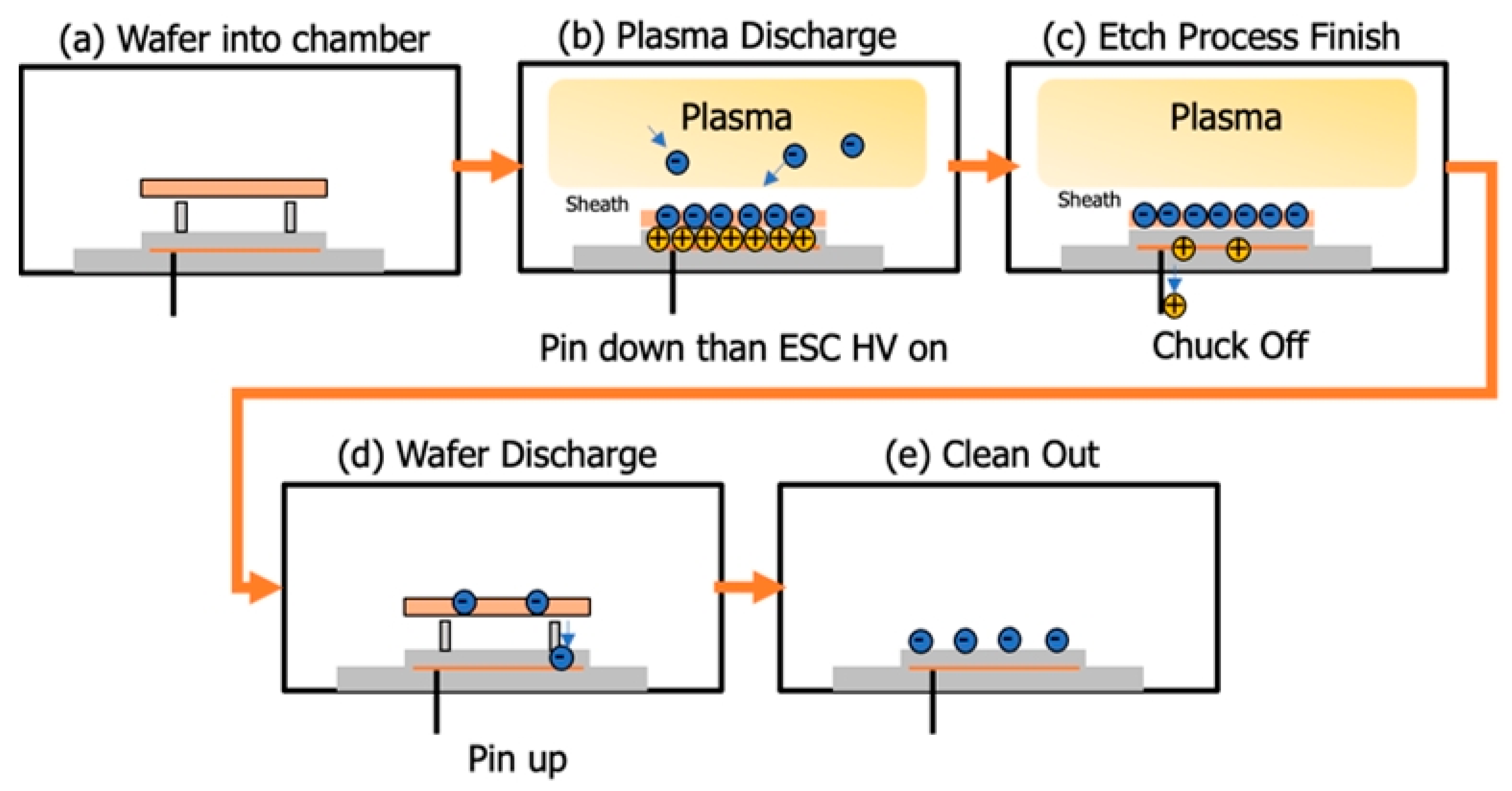
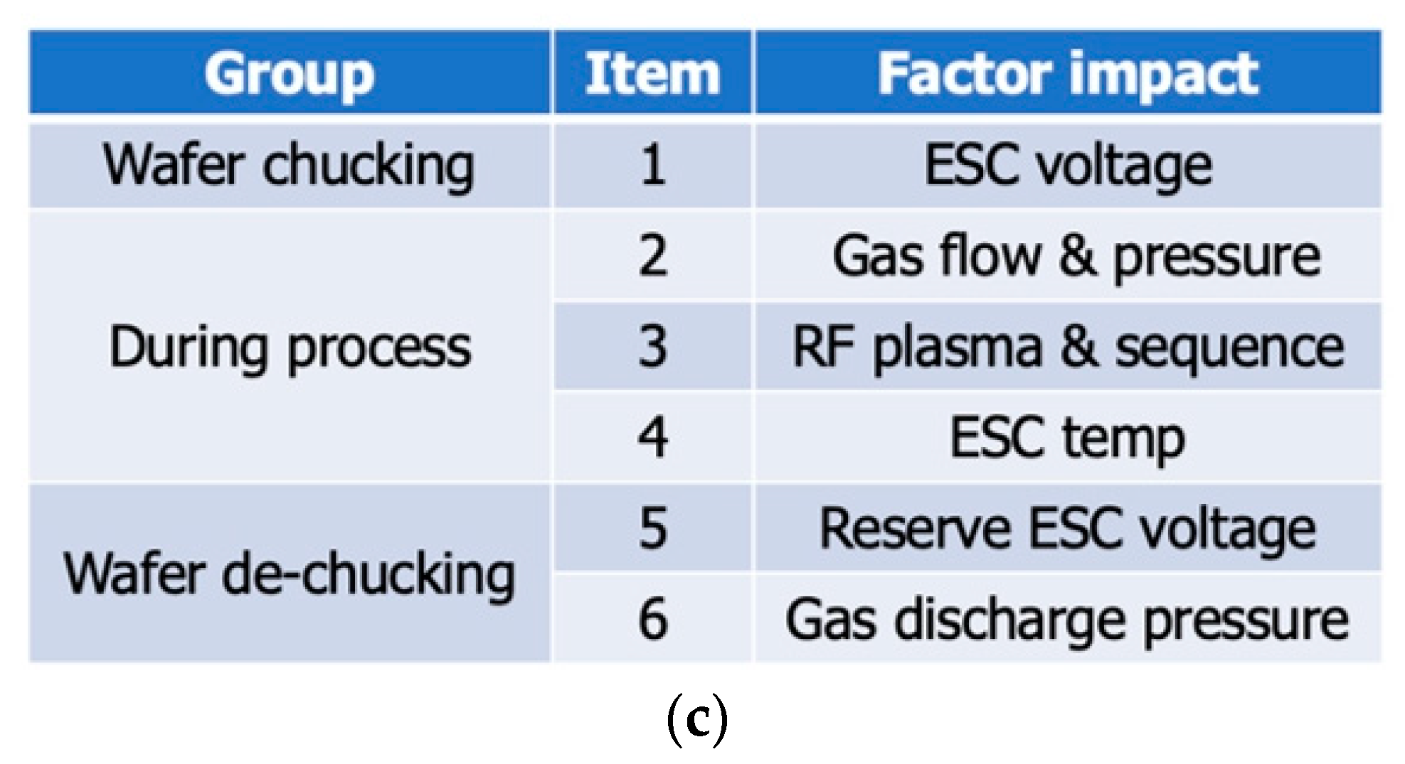
3. Control Strategy and Experiment

A CCP etching system was used in the experiments conducted in this study. This system could generate high-density plasma and free radicals for dry etching. The bottom electrode was connected to an RF power output to generate plasma for the etching process and to control the acceleration of ions on the wafer surface. The upper electrode was applied with a DC voltage, and the plasma density was controlled by adding the DC voltage (Figure 2).
The operating range of the chamber pressure was 10 to 800 mTorr. The pressure was regulated by controlling the gas flow from a gas diffusion plate by using a flow control system. The temperature of the top electrode could be set to a maximum value of approximately 150 °C. As shown in Figure 3, an ESC was used to fix the wafer during the dry etching process, and an electrode plate with a high DC voltage was used to generate the chucking force. Helium gas was allowed to flow through holes distributed on the surface of the ESC into the back side of the wafer to control the wafer’s temperature. A liquid flowing through the ESC cooling path was used for external temperature control to regulate the process temperature.
The chucking force is a key factor affecting the performance of the ESC. This force is influenced by the voltage applied to the ESC, the properties of the dielectric layer of the ESC, and the geometric structure of the ESC. The Coulomb force of the ESC (i.e., the chucking force) is expressed as follows:
F = 1 2 ε 0 A ( kU h ) 2
where A is the electrode area, ε 0 is the permittivity of free space, k is the relative permittivity, U is the applied voltage, and h is the distance between the bottom surface of the wafer and the top surface of the ESC [27]. The distance h is equal to the combined thickness of the dielectric layer d with a relative permittivity of kd and the gas layer g with a relative permittivity of kg. The sandwich structure formed by these layers can be considered as a structure containing two capacitors connected in series. By substituting for h in Equation (5), the chucking force can be expressed as follows:
F = 1 2 ε 0 A ( k d k g U k g d + k d g ) 2
where kg ≈ 1 if g d , which occurs in most cases. By using this approximation, the following equation is derived:
F = 1 2 ε 0 A ( k d U d + k d g ) 2
Equation (7) reveals that the chucking force is directly dependent on the properties of the dielectric material (kd) and the layer thickness (d). Thinner dielectric layers can be used to achieve a higher chucking force.
In the conducted experiments, the effects of polluting particle sources and driving forces were investigated. We first opened the chamber with the most wafer particles for maintenance to identify the parts of the chamber in which particle sources caused deposition. Powder was then collected from the by-products in the turbo pump exhaust line, as shown in Figure 4a. Next, we sprayed powder (fluorine and titanium) on the surfaces of related parts (i.e., the top electrode, edge ring, chamber wall, exhaust plate in the chamber, and other parts) to simulate a worst-case particle deposition scenario. A silicon wafer was used to check the particle contamination in the chamber. The wafer experiment method was performed through the wafer transfer only condition, and then using the following process parameter conditions as an N2 gas flow rate of 200 sccm (wafer chucking step using gas), a maximum RF power of 500 W, and an ESC voltage of 2500 V (Figure 4b). In all conditions except that involving the wafer transfer only condition, the chamber pressure was adjusted to 50 mTorr within 60 s through gas flow control. The process was then performed in the etching chamber for approximately 10 s, the effects of the number of particles caused by gas flow on the wafer surface, a high ESC voltage, and the RF plasma driving force were verified over more than 200RFhrs in the chamber (Figure 4c). After the wafering process was completed, the number of particles on the silicon wafer was measured using an optical wafer surface inspection device (KLA-Tencor Surf-scan SP2). The particle measurements were set as 0.06 µm.

4. Results and Discussion

The results obtained in eight experimental procedures under 12 particle test conditions are described in the following text.

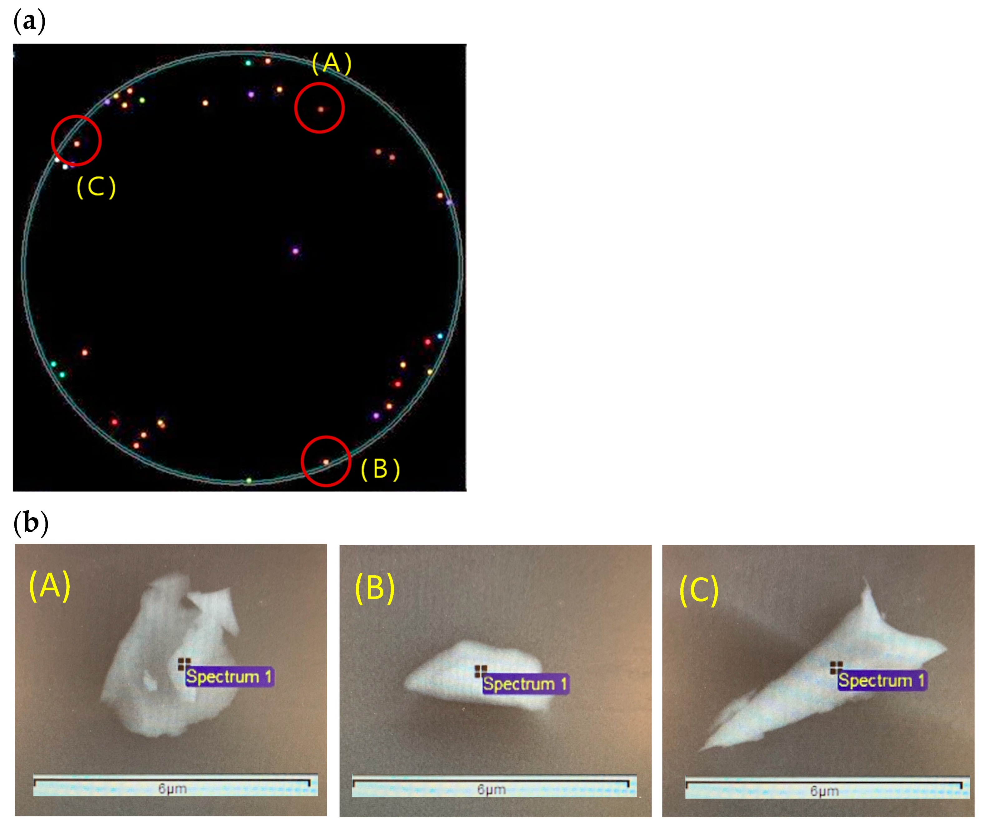
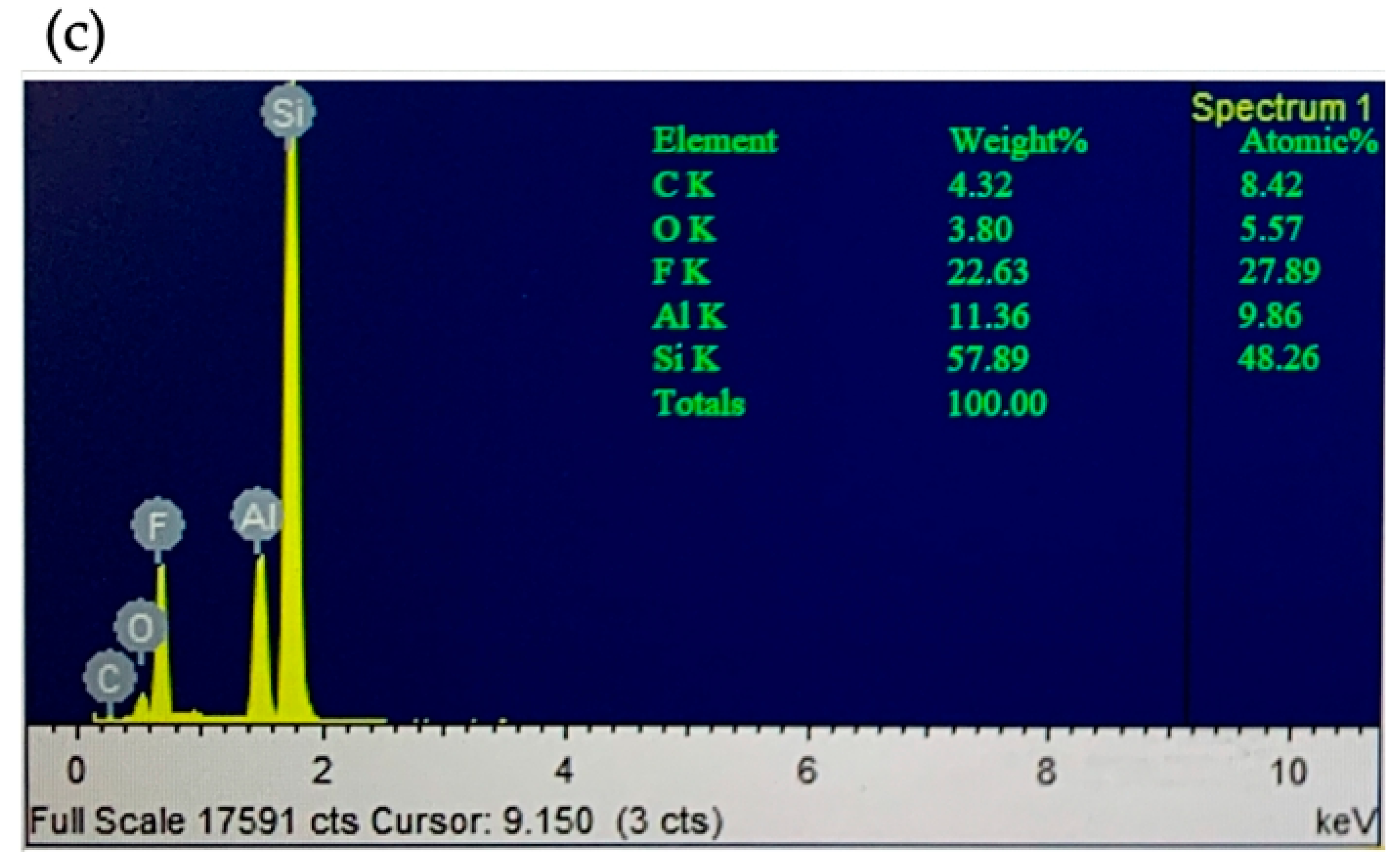
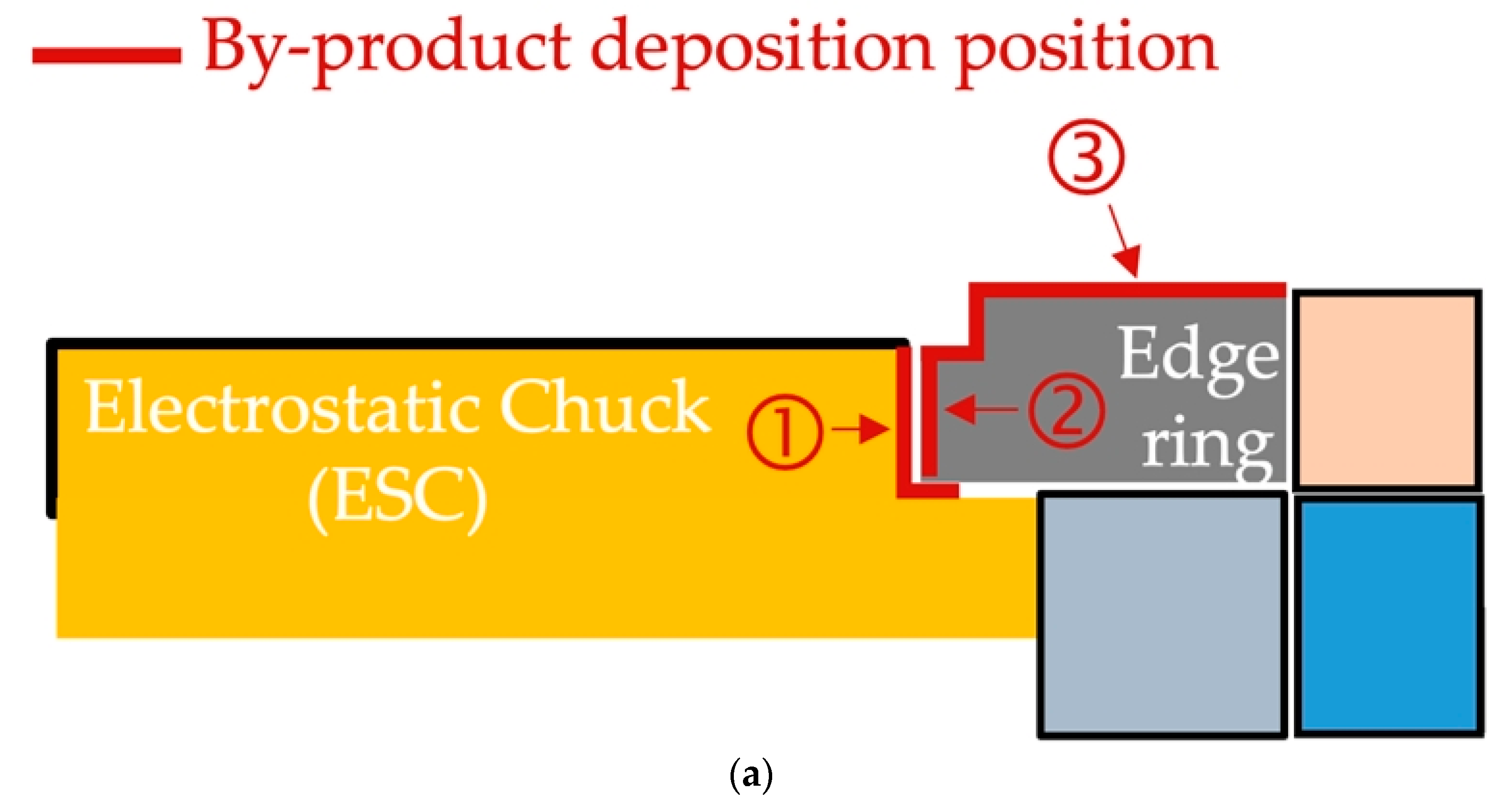
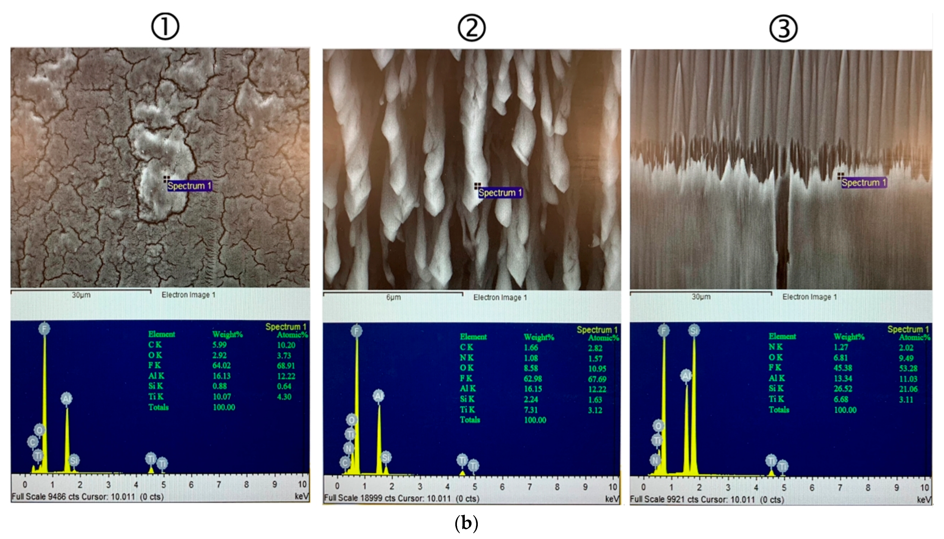
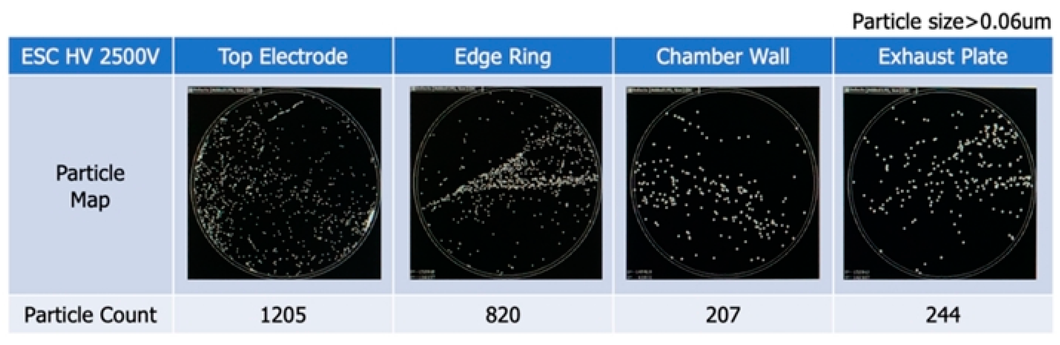
4.1. Particle Sources Verified through Chamber By-Product Deposition Analysis

Figure 5a presents the chamber by-products deposited around the ESC and edge ring after 225 h in the RF chamber. The deposited chamber by-products were analyzed through scanning electron microscopy (SEM) and energy-dispersive X-ray spectroscopy (EDX), as displayed in Figure 5b. Surface deposition areas from 6 to 30 μm could be detected through SEM. The EDX spectra were used to analyze the percentage concentration of each element in the deposition. In Figure 5, the y-axis indicates the number of X-rays, and the x-axis indicates the energy of the X-rays. The EDX spectra contained yellow peaks corresponding to all the elements in the deposited by-products. The positions of the peaks revealed that fluorine, aluminum, and oxygen were present in the deposited by-products, and the peak heights were used to determine the concentration of each element. The composition of the deposited by-products was similar to the edge particle composition. We determined that the particles originated from the deposition occurring at the ESC side wall and edge ring.

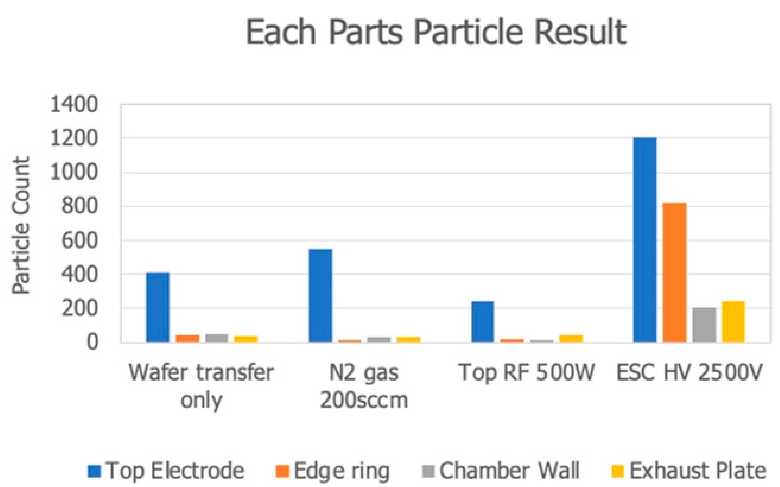
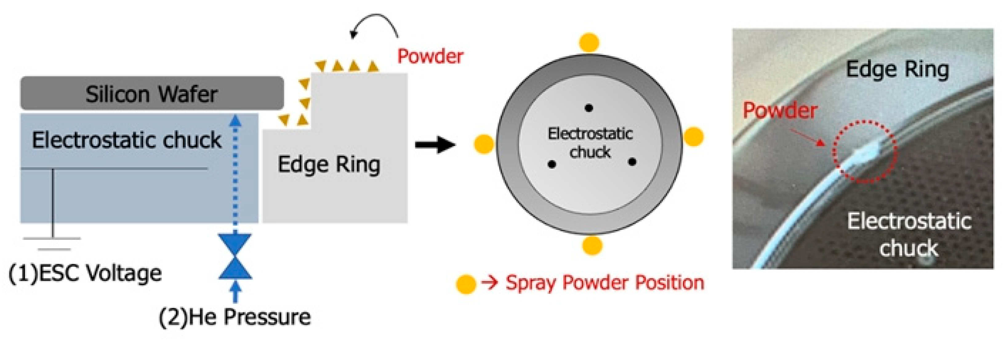
4.2. Particle Results for Each Wafer Test Condition in Which Powder Was Placed on the Surface of Each Part in the Chamber

Figure 6 reveals that numerous wafer particles were formed under the wafer transfer only, an N2 gas flow rate of 200 sccm, a maximum RF power of 500 W, and an ESC voltage of 2500 V when powder was sprayed on the top electrode’s surface. Particles were suspended and fell onto the wafer because of the turbulence of the flow field caused by the gas, or the electric field generated by the RF plasma and ESC. For powder sprayed on the surface of any part in the chamber, the number of wafer particles produced when the ESC voltage was 2500 V was higher than that produced under any other condition. The particle and edge maps revealed a random particle distribution when the ESC voltage was 2500 V. The ESC voltage appeared to affect the movement of particles to the wafer surface. As presented in Figure 7, the maximum particle count on the wafer was 1205 when the ESC voltage was 2500 V.

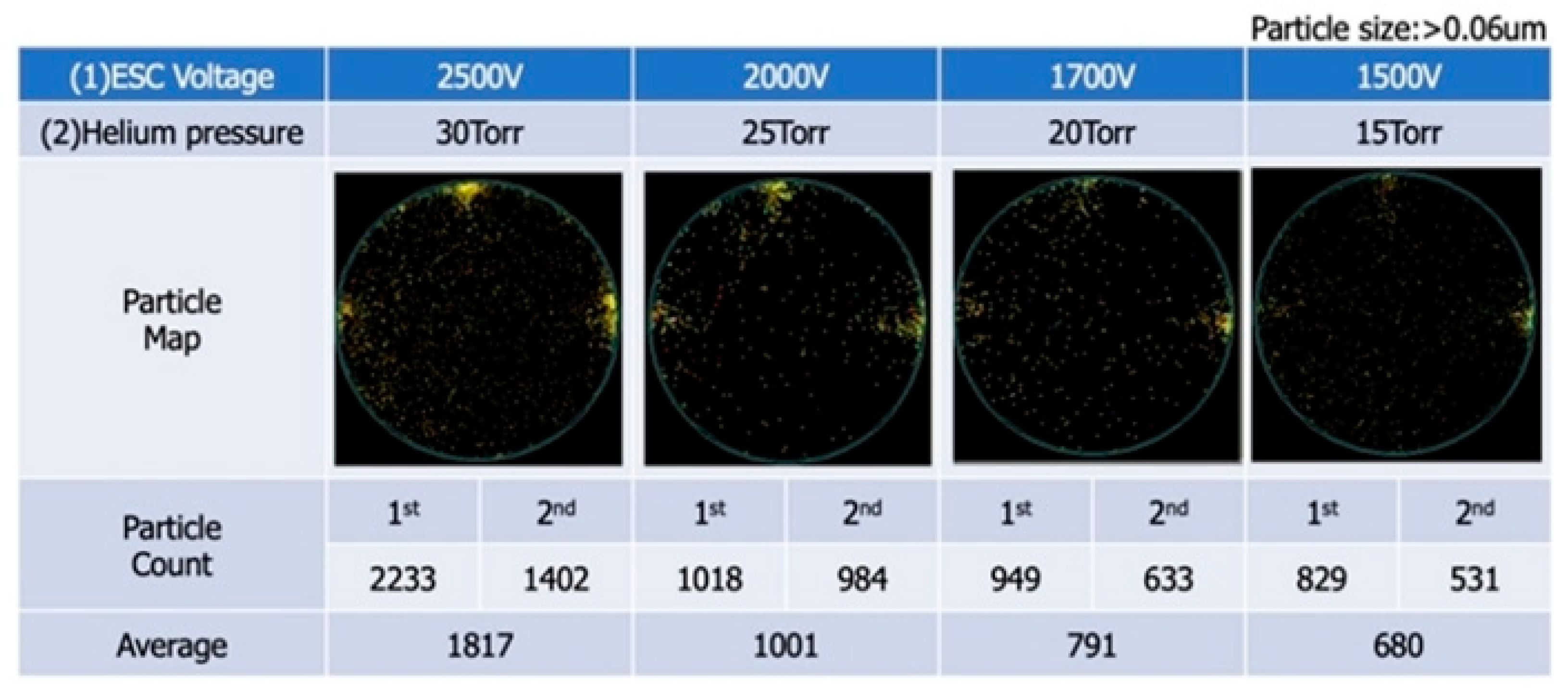
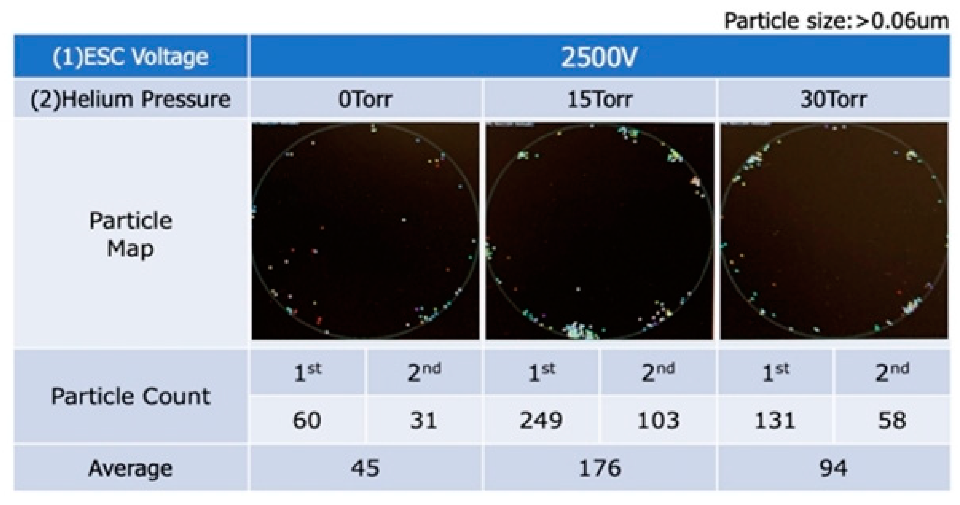
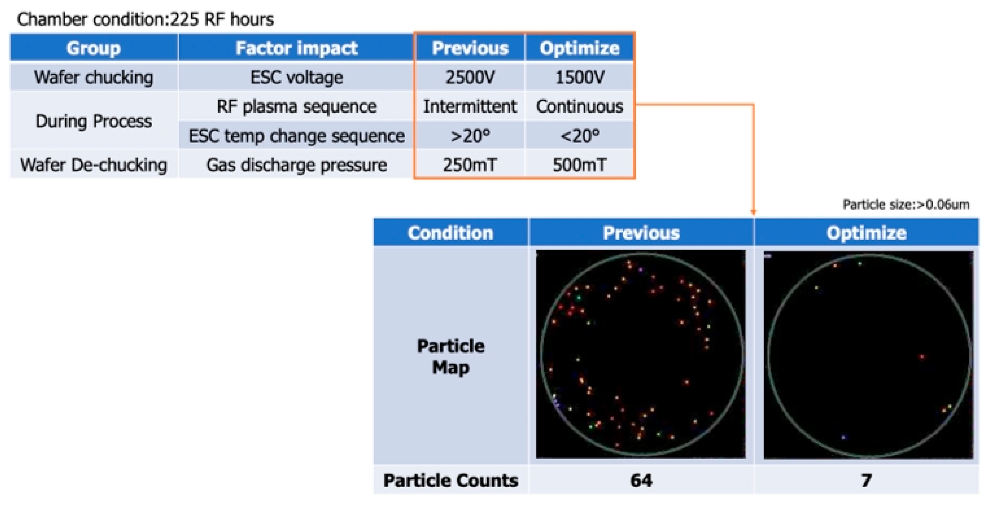
4.3. ESC Voltage and Helium Pressure Control

To verify that the ESC voltage caused a large number of particles to be generated on the wafer surface, we sprayed powder on the surface of the edge ring around the ESC to simulate worst-case particle deposition conditions. In the experimental process, the ESC voltage was set to four conditions of 2500 V, 2000 V, 1700 V, and 1500 V to reduce the chucking force of the wafer to analyze and verify the number of particle contamination, as shown in Figure 8. The experimental results are shown in Figure 9. As the setting of the ESC voltage output parameter decreased, the particle contamination on the wafer also reduced. Therefore, the electric field, which varies with the ESC voltage output, is closely related to the number of suspended particles. Therefore, not only the electric field generated by the radio frequency discharge will cause the particles to be suspended. In the case of the ESC output voltage, particles also caused a suspension mechanism. On the other hand, in order to verify whether the number of particles is also related to the helium pressure of the ESC voltage, we performed experiments at the same ESC voltage of 2500 V using helium pressures of 0, 15, and 30 Torr. From the particle map results in Figure 10, it is shown that the size of the helium pressure does not affect the number of particles. Therefore, using a lower ESC voltage (i.e., lower chucking force) during wafer processing can reduce particle deposition on the wafer.

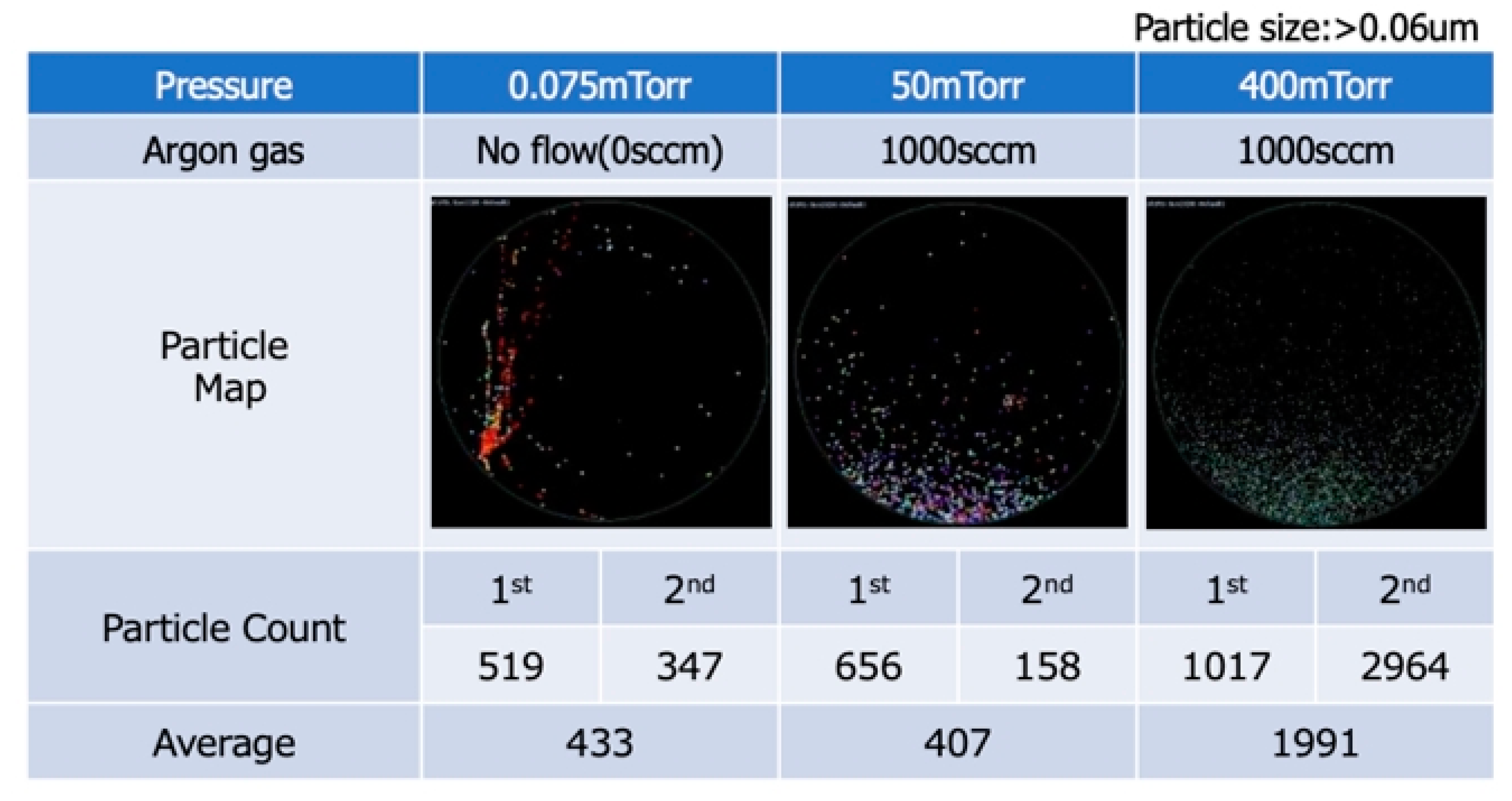
4.4. Particle Distributions for Different Gas Flows and Pressures

The particles deposited on the wafer were analyzed under different gas flow and pressure control conditions. To control the argon gas flow (wafer process step using gas), the chamber pressure was set as 0.075 mTorr, with the argon gas no flow as 0 sccm. Alternatively, the chamber pressure was set as 50 or 400 mTorr, with the argon gas flow set as 1000 sccm. The process time was 10 s. Figure 11 presents a partial particle map for the wafer edge. This map reveals that the particle count was high when the chamber pressure was 400 mTorr and the argon flow rate was 1000 sccm. Thus, a higher chamber pressure and gas flow rate result in higher particle counts when the process time is fixed as 10 s.

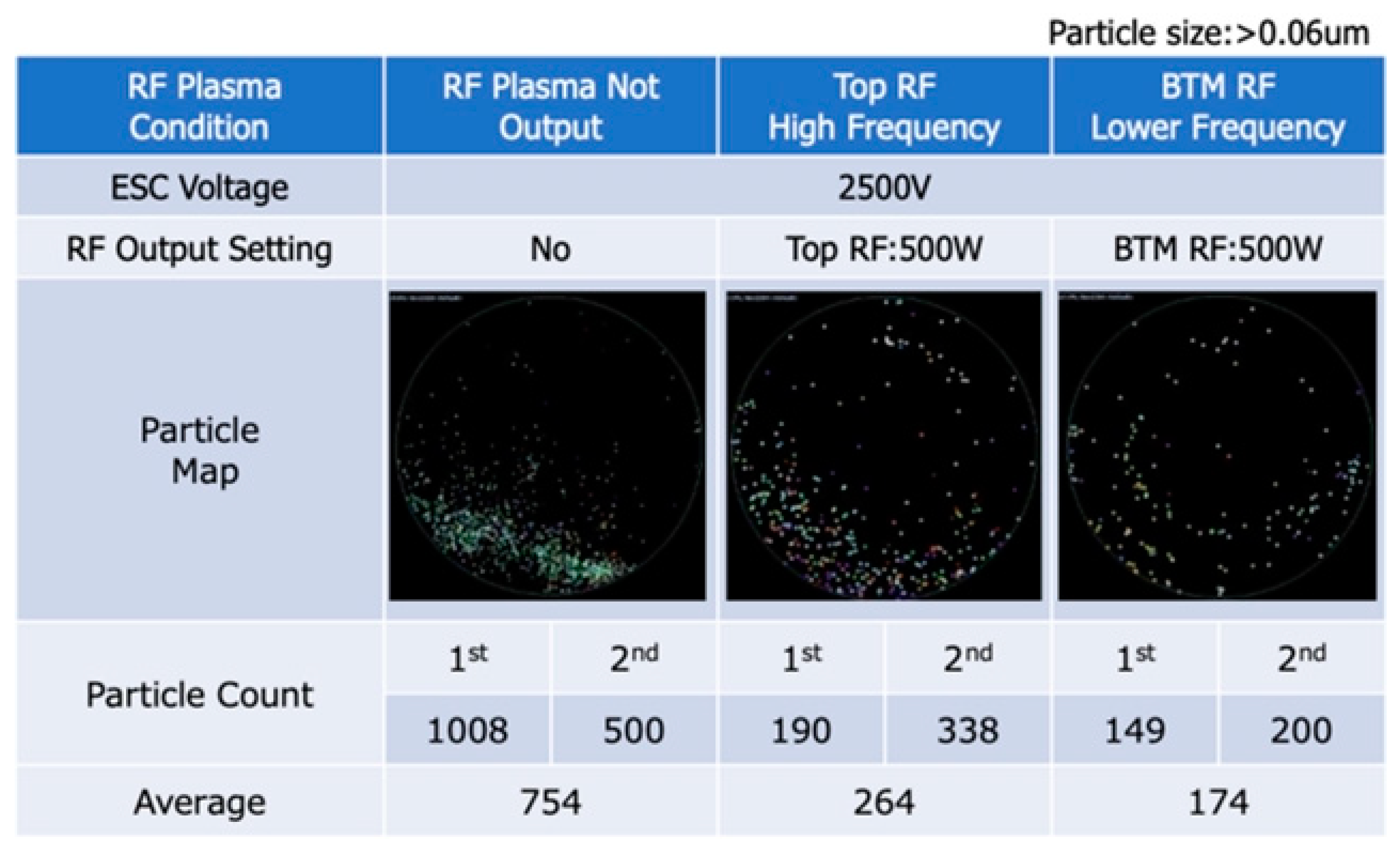
4.5. Particle Distribution Results under Different RF Plasma Discharge Conditions during Wafer Processing

The effect of different RF plasma discharge conditions on wafer particles was analyzed. The RF plasma power was set as no output, high RF (high frequency) at 500 W, or BTM RF (low frequency) at 500 W. The chamber pressure was set as 200 mTorr, the argon gas flow rate was set as 1000 sccm, and the process time was 10 s. Figure 12 reveals that discharge without an RF power output resulted in the production of more particles than did discharge with high- or low-frequency RF power. The results indicate that the plasma sheath generated during high- and low-frequency plasma output may prevent particles from falling onto the wafer.

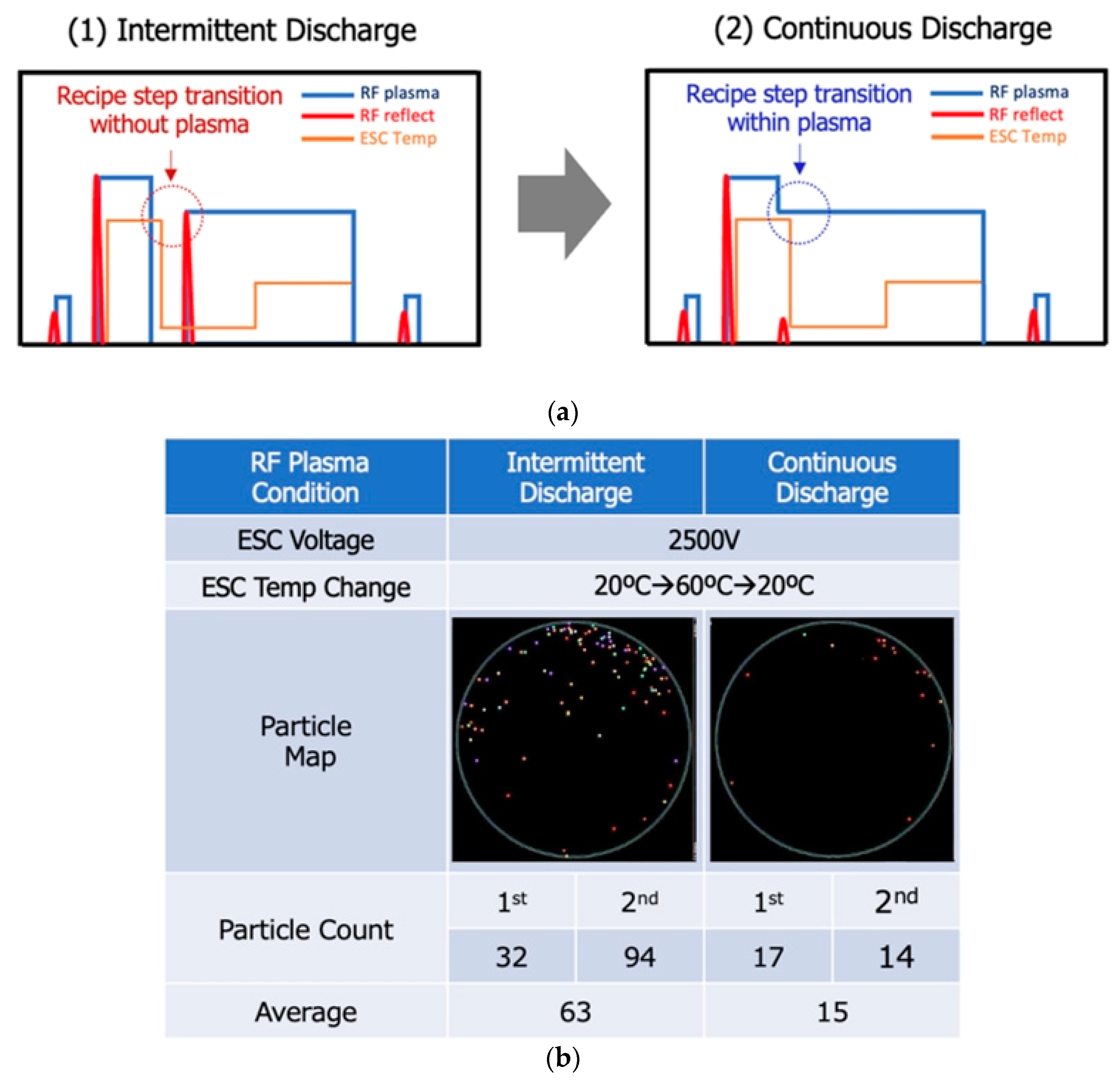
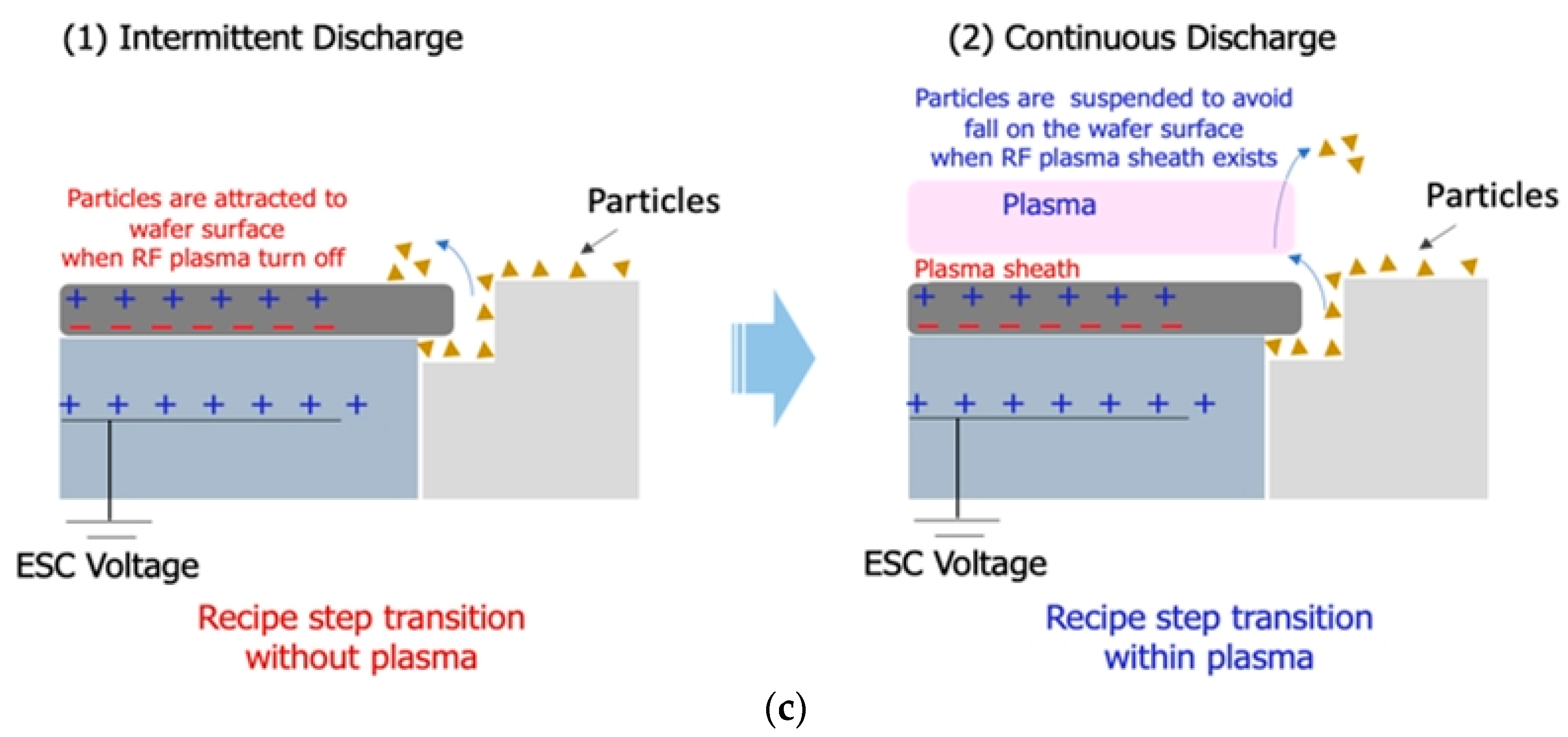
4.6. Particle Distribution Results for Different RF Plasma Discharge Sequences

We examined the effects of intermittent or continuous plasma discharge on the particles on the wafer, as shown in Figure 13a. The particle map in Figure 13b presents a comparison of the particle numbers under intermittent and continuous discharge. The particle result shows that the continuous discharge by the RF plasma method reduces the number of particles. Step transitions within the plasma sheath suppress the particles. Intermittent plasma discharges result in higher particle counts than do continuous plasma discharges because particles are attracted to the wafer’s positive potential surface when the RF plasma flow is turned off. We observed that the plasma sheath prevented the particles from being attracted to the wafer surface when the particles were negatively charged and suspended in the plasma-on chamber. Therefore, the continuous discharge sequence of RF plasma can reduce particle adhesion to the wafer, as depicted in Figure 13c.

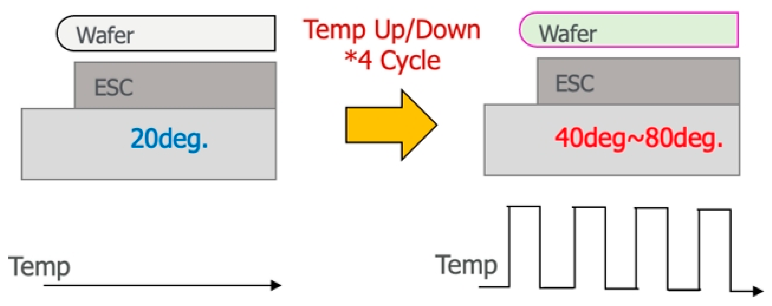
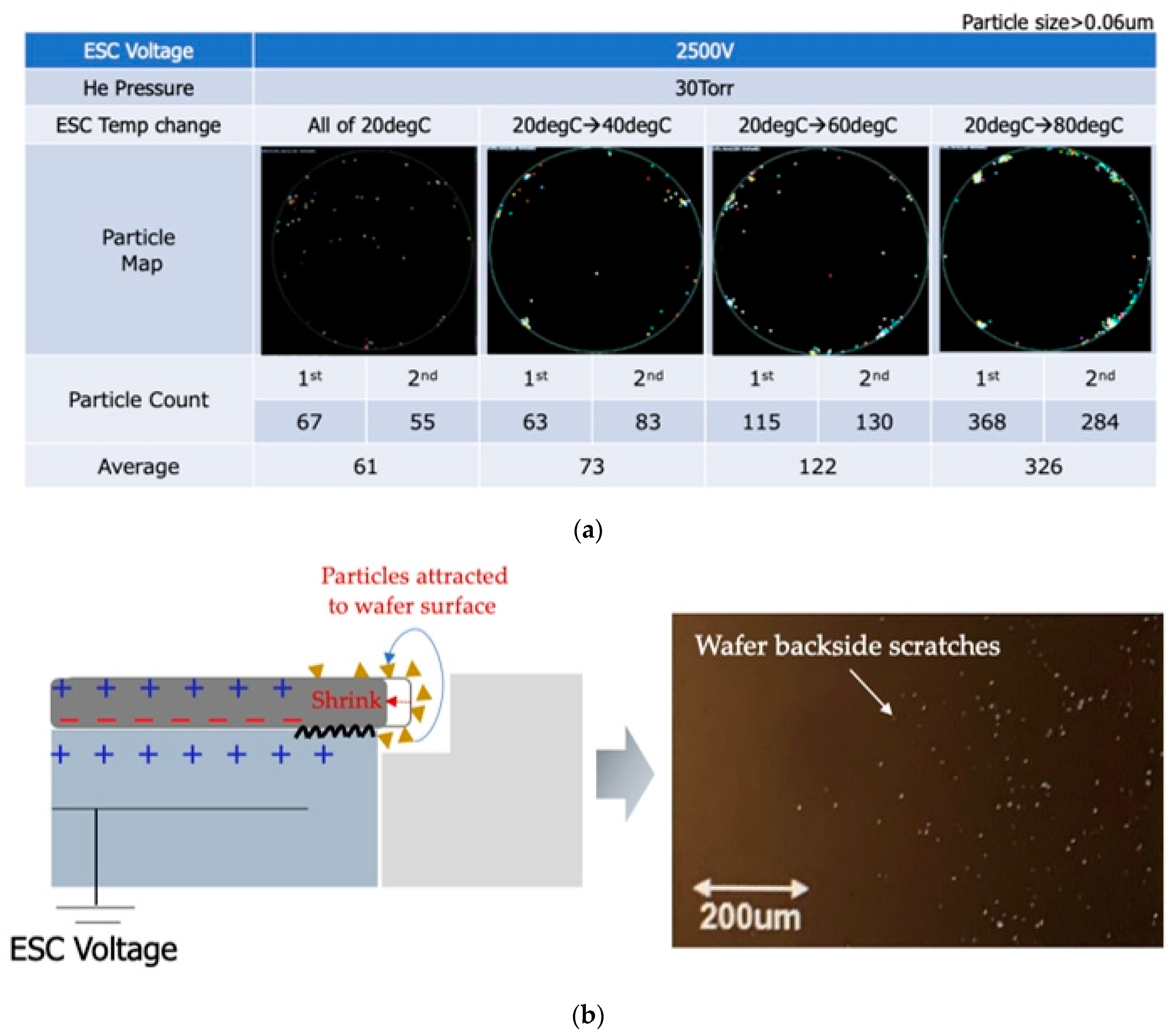
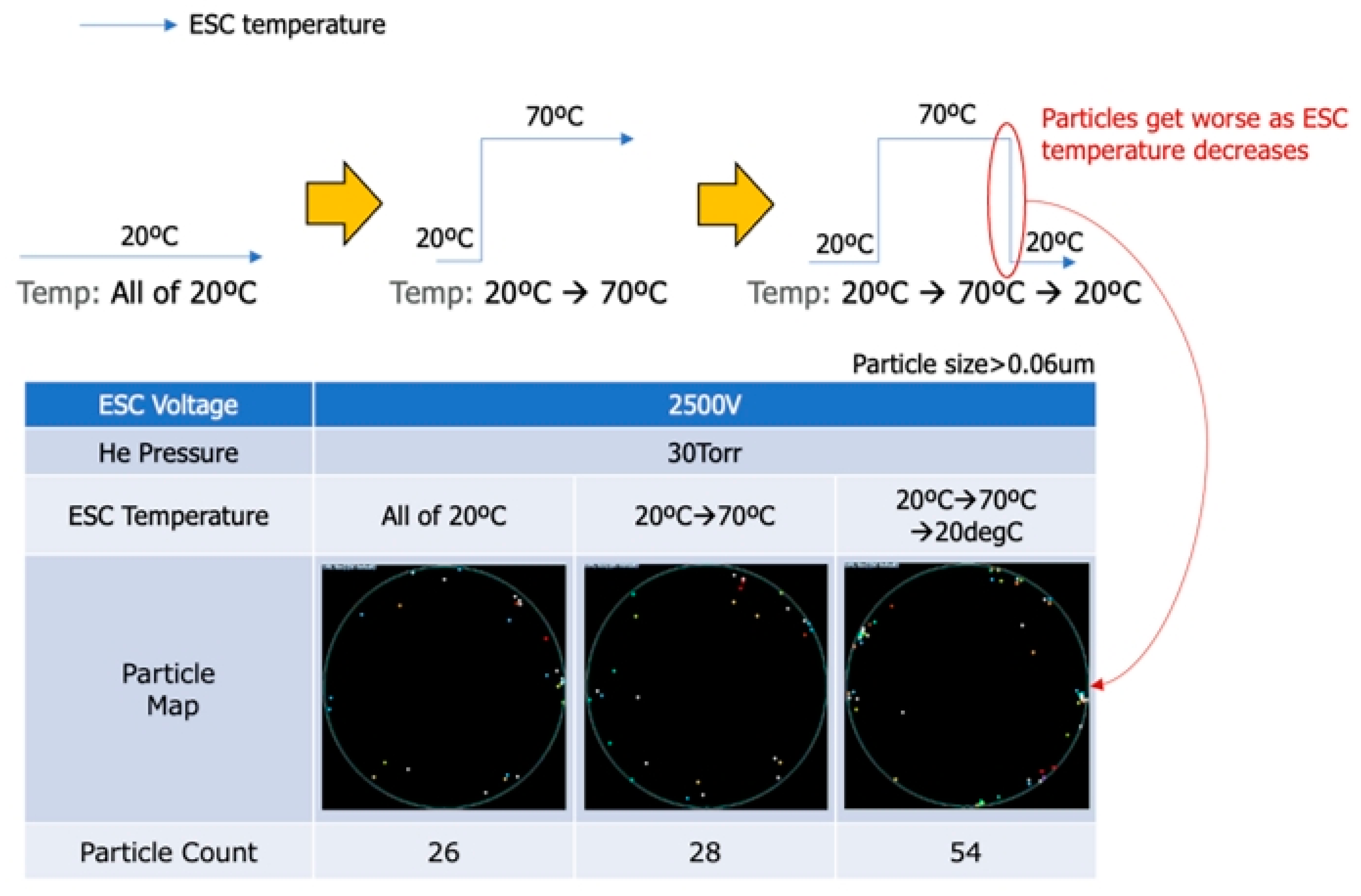
4.7. Temperature of the ESC

The correlation between changes in the temperature of the ESC and particle contamination during the etching process was analyzed. The ESC had a fixed voltage of 2500 V, and its temperature was set as 20, 40, 60, and 80 °C in the experiments. Four temperature cycles were tested in each experiment, and no plasma was produced. For each temperature condition, two wafers were used, as displayed in Figure 14. Figure 15a reveals that relatively few particles were produced under temperature changes of less than 20 °C. If the temperature change was higher than 20 °C, edge particles were generated on the wafer. These particles are attributed to the scratches on the back side of the wafer caused by thermal expansion during the ESC heating cycle. The particles were attracted to the wafer surface because of the positive potential of the ESC and finally adhered to the edge of the wafer, as depicted in Figure 15b. The aforementioned thermal expansion can be expressed as follows:
L = L 0 ( 1 + a · Δ T )
where L is the length after expansion, L0 is the length before expansion, ΔT is the temperature difference, and a is the coefficient of thermal expansion (2.6 × 10⁻⁶ K−1 for silicon). The related frictional force is expressed as follows:
F = μ × w
where μ is the coefficient of friction, and w is the normal force (=mg + F, where m is the weight of the silicon wafer, and g is the chucking force). Thermal expansion and contraction of the wafer results in friction between the wafer and the surface of the ESC. The effects of temperature on the ESC were analyzed, and temperature was found to be a key factor affecting the particle count. The particle map presented in Figure 16 reveals that decreases in temperature resulted in increases in the particle count. This result is attributed to particles on the backside of the wafer traveling to the front side when the temperature was reduced.

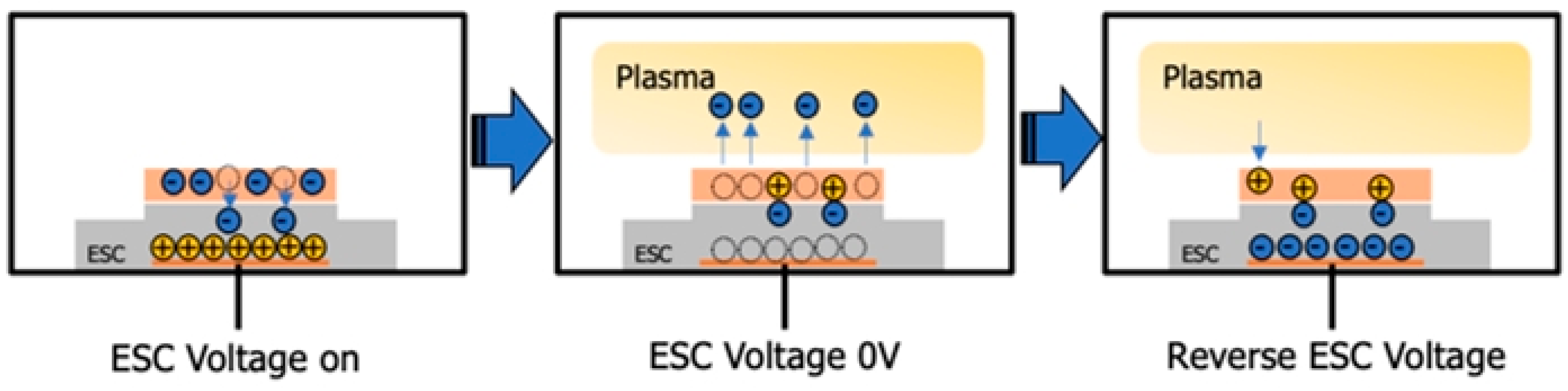
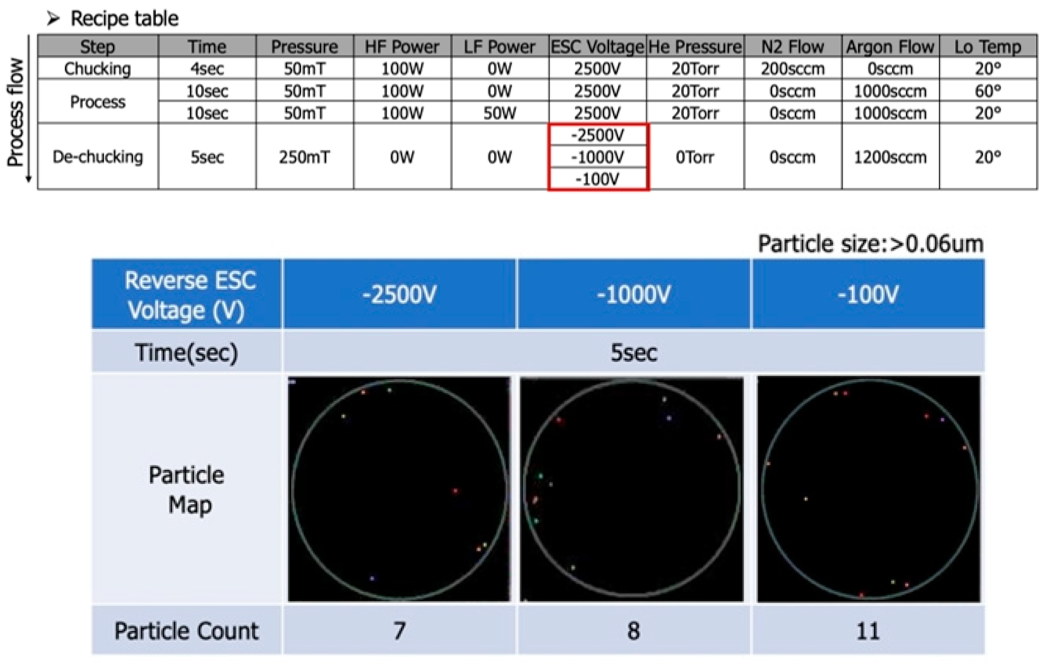
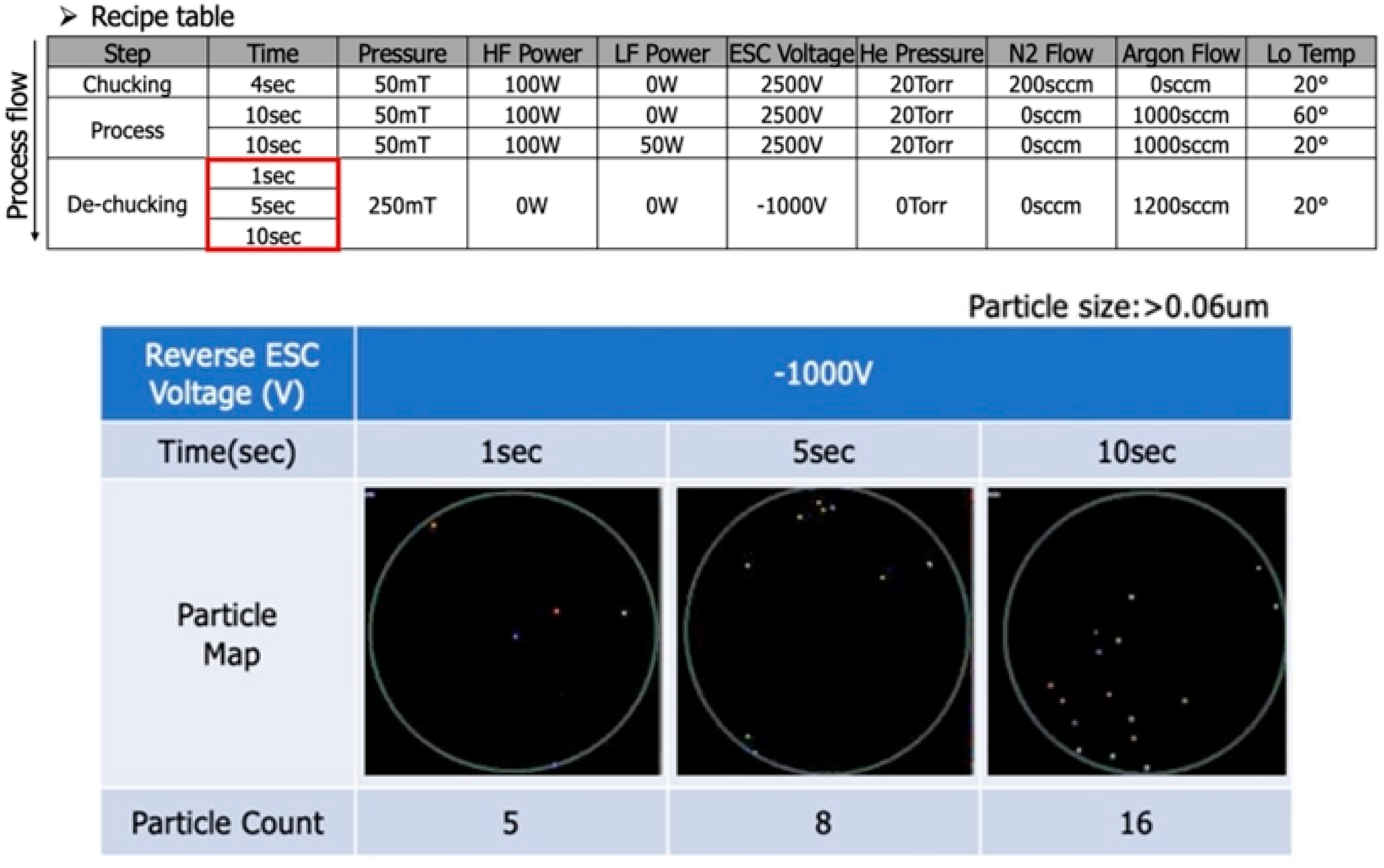
4.8. ESC Voltage Reversal during the Wafer De-Chucking Step

A reverse voltage was used to neutralize the remaining charge in the wafer de-chucking step. The effect of different reverse voltages in the neutralization step on particle deposition was investigated. The reverse voltage was set as −2500, −1000, or −100 V. The opening time was set as 5 s, and the wafer residual charge was neutralized by applying a reverse voltage. Figure 17 illustrates the neutralization process in the wafer de-chucking step.
Figure 18 reveals that a reverse voltage of −100 V resulted in marginally higher particle deposition than did the other reverse voltages. Nevertheless, the particle deposition results for the three reverse voltages were similar, and whether particle counts are correlated with changes in the reverse voltage is unclear.
In accordance with the aforementioned results, the reverse voltage was set as −1000 V, and the voltage application time was set as 1, 5, or 10 s to analyze the effects of this time on the particle distribution on the wafer surface. Figure 19 reveals that a longer application time for the ESC reverse voltage resulted in higher wafer particle deposition. A longer application time for an ESC reverse voltage caused higher potential changes, and the particles were first suspended before adhering to the wafer.

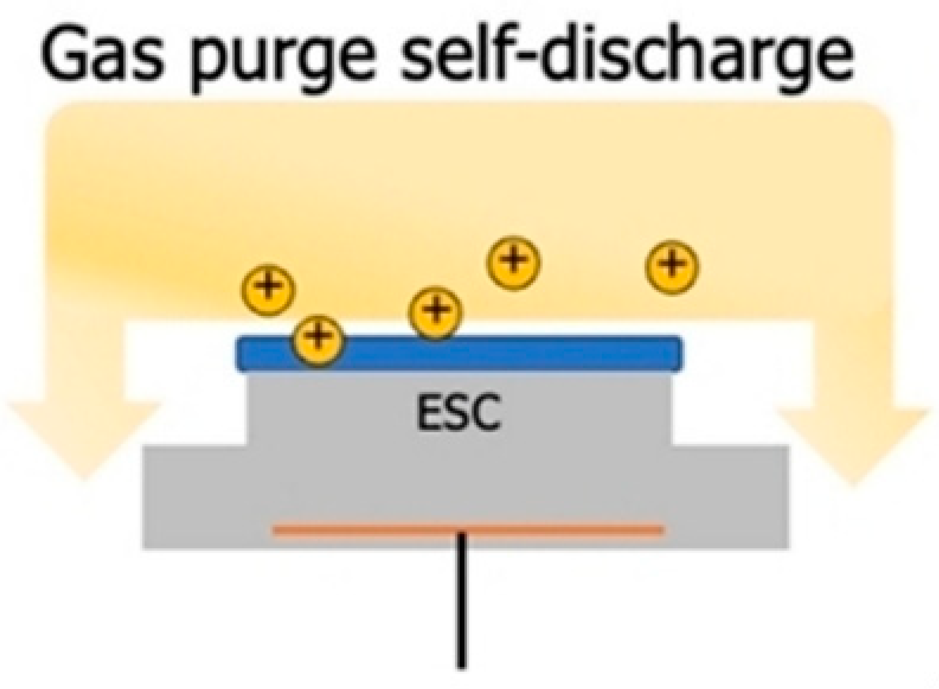
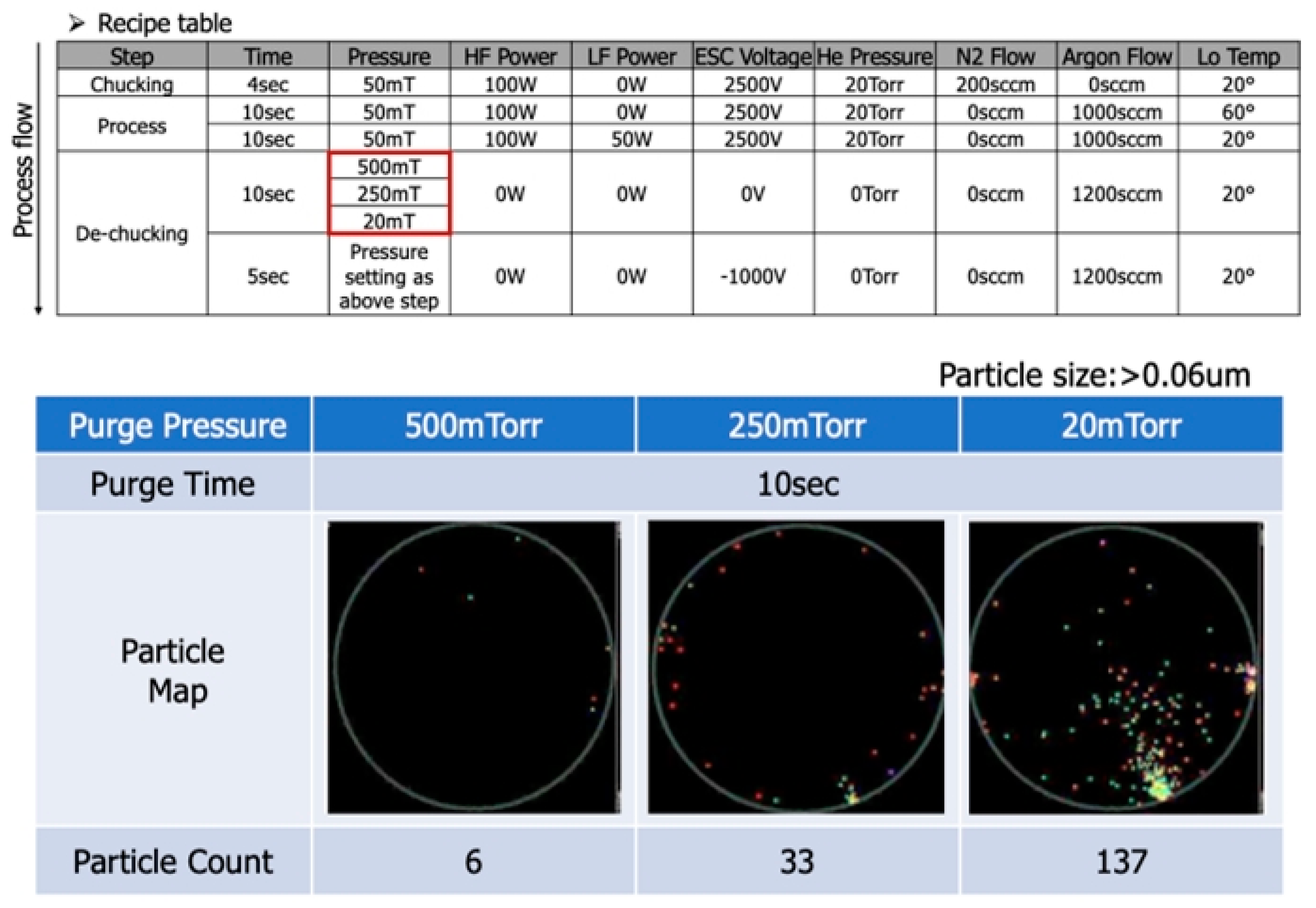
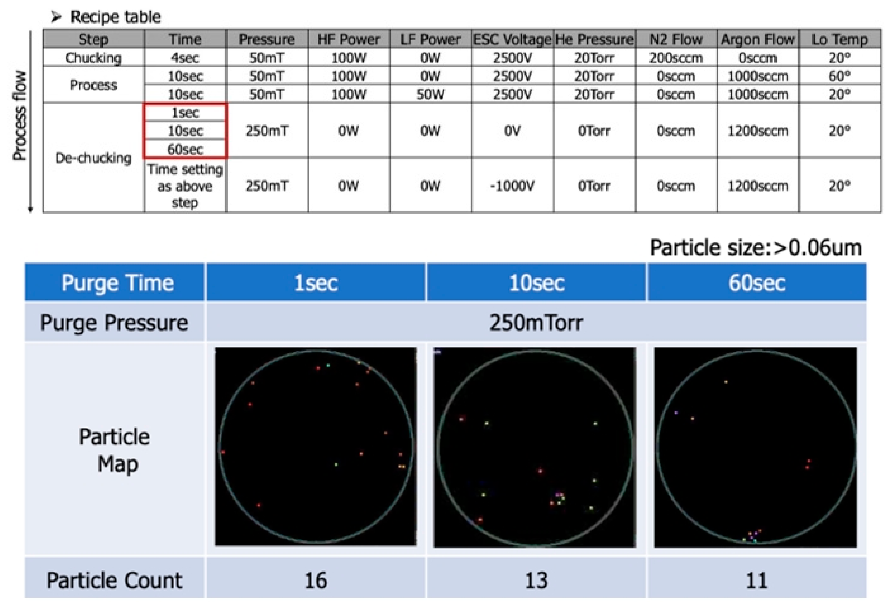
4.9. Gas Purge Discharge Pressure Control during Wafer De-Chucking

In addition to using the different reverse voltages used in the wafer de-chucking step for the effect of particle analysis, this experimental condition to use the control of gas purge discharge pressure was also controlled to perform for conducting a particle effect analysis. An experiment was conducted in which the gas purge discharge pressure was controlled during the wafer de-chucking step (Figure 20). First, the purge pressure was set as 20, 250, or 500 mTorr, and the process time was fixed as 10 s. Figure 21 reveals that the highest particle count was observed at 20 mTorr; higher pressures resulted in lower particle counts. On the basis of this result, the effects of discharge times of 1, 10, and 60 s at 250 mTorr were investigated. The particle count was marginally higher under a discharge time of 1 s than under the other discharge times, as shown in Figure 22.

5. Conclusions

In this study, we investigated the effects of the voltage and temperature of an ESC on the number of edge particles produced. We compared the effects of intermittent and continuous plasma discharge sequences, various gas flow rates, and pressure changes on edge particle contamination on silicon wafers during the etching process, as shown in Figure 23. The particle map results revealed that if the RF power was turned off at process step transitions, particles were attracted to the remaining positive charge on the wafer surface. When RF power was applied during process step transitions, a plasma sheath was generated. This sheath prevented particles from being attracted to the wafer surface. During the wafer chucking process, high chuck voltages and large differences in the temperature of the ESC promoted the generation of edge particles. Thus, the source of edge particle contamination is a by-product existing around the ESC. The particles of this by-product are suspended on the wafer surface because of imperfect process settings. Negatively charged particles are attracted by the positive potential of the ESC, and the number of attracted particles depends on the magnitude of the positive charge potential. Therefore, differences in the wafer surface potential result in edge particle contamination. We conclude that optimizing the wafer chucking step and process conditions by controlling the temperature changes of the ESC and the sequence of the RF plasma discharge can effectively reduce the number of edge particles generated on dry etching equipment during the oxide layering process.

Author Contributions

Conceptualization, C.-M.K. and S.C.; Methodology, C.-M.K.; Validation, C.-M.K.; Formal Analysis, C.-M.K. and S.C.; Investigation, C.-M.K.; Resources, C.-M.K.; Data Curation, C.-M.K. and S.C.; Writing—Original Draft Preparation, C.-M.K. and S.C.; Writing—Review and Editing, C.-M.K. and S.C.; Supervision, S.C.; Project Administration, C.-M.K. and S.C. All authors have read and agreed to the published version of the manuscript.

Funding

This research received no external funding.

Institutional Review Board Statement

Not applicable.

Informed Consent Statement

Not applicable.

Data Availability Statement

Not applicable.

Conflicts of Interest

The authors declare no conflict of interest.

References

  1. Selwyn, G.S.; Heidenreich, J.E.; Haller, K.L. Particle trapping phenomena in radio frequency plasmas. Appl. Phys. Lett. 1990, 57, 1876. [Google Scholar] [CrossRef]
  2. Selwyn, G.S.; Heidenreich, J.E.; Haller, K.L. Rastered laser light scattering studies during plasma processing: Particle contamination trapping phenomena. J. Vac. Sci. Technol. A 1991, 9, 2817. [Google Scholar] [CrossRef]
  3. Sommerer, T.J.; Barnes, M.S.; Keller, J.H.; McCaughey, M.J.; Kushner, M.J. Monte Carlo-fluid hybrid model of the accumulation of dust particles at sheath edges in radio-frequency discharges. Appl. Phys. Lett. 1991, 59, 638. [Google Scholar] [CrossRef] [Green Version]
  4. Barnes, M.S.; Keller, J.H.; Forster, J.C.; O’Neill, J.A.; Coultas, D.K. Transport of dust particles in glow-discharge plasmas. Phys. Rev. Lett. 1992, 68, 313. [Google Scholar] [CrossRef] [PubMed]
  5. Watanabe, Y.; Shiratani, M.; Yamashita, M. Observation of growing kinetics of particles in a helium-diluted silane RF plasma. Appl. Phys. Lett. 1992, 61, 1510. [Google Scholar] [CrossRef]
  6. Sato, N.; Uchida, G.; Kaneko, T.; Shimizu, S.; Iizuka, S. Dynamics of fine particles in magnetized plasmas. Phys. Plasmas 2001, 8, 1786. [Google Scholar] [CrossRef]
  7. Blain, M.G.; Tipton, G.D.; Holber, W.M.; Selwyn, G.S.; Westerfield, P.L.; Maxwell, K.L. Particle behaviour in an electron cyclotron resonance plasma etch tool. Plasma Source Sci. Technol. 1994, 3, 325. [Google Scholar] [CrossRef]
  8. Fukuzawa, T.; Obata, K.; Kawasaki, H.; Shiratani, M.; Watanabe, Y. Detection of particles in rf silane plasmas using photoemission method. J. Appl. Phys. 1996, 80, 3202. [Google Scholar] [CrossRef]
  9. Tan, C.M.; Luo, M.; Leng, I.C.H. Maintenance scheduling of plasma etching chamber in wafer fabrication for high-yield etching process. IEEE Trans. Semicond. Manuf. 2014, 27, 204–211. [Google Scholar] [CrossRef]
  10. Burghard, R.; Moriya, T.; Matsuzaki, K.; Nagaike, H.; Nakayama, H. (Eds.) In Situ Particle Monitors: The Next Level of Yield Control for Critical Processes. In Proceedings of the 2006 IEEE International Symposium on Semiconductor Manufacturing, Tokyo, Japan, 25–27 September 2006. [Google Scholar]
  11. Uesugi, F.; Ito, N.; Moriya, T.; Doi, H.; Sakamoto, S.; Hayashi, Y. In situ monitoring of particles generated in tungsten etch-back processing. J. Vac. Soc. Jpn. 1998, 41, 776–781. [Google Scholar] [CrossRef]
  12. Uesugi, F.; Ito, N.; Moriya, T.; Doi, H.; Sakamoto, S.; Hayashi, Y. Observation of the trajectories of particles in process equipment by an insitu monitoring system using a laser light scattering method. J. Vac. Sci. Technol. B 1998, 16, 3339. [Google Scholar] [CrossRef]
  13. Uesugi, F.; Ito, N.; Moriya, T.; Doi, H.; Sakamoto, S.; Hayashi, Y. Real-time monitoring of scattered laser light by a single particle of several tens of nanometers in the etching chamber in relation to its status with the equipment. J. Vac. Sci. Technol. A 1998, 16, 1189. [Google Scholar] [CrossRef]
  14. Moriya, T.; Nagaike, H.; Denpoh, K.; Morimoto, T.; Aomori, M.; Kawaguchi, S.; Shimada, M.; Okuyama, K. Observation and evaluation of flaked particle behavior in magnetically enhanced reactive ion etching equipment using a dipole ring magnet. J. Vac. Sci. Technol. B 2004, 22, 1688–1693. [Google Scholar] [CrossRef]
  15. Selwyn, G.S.; Singh, J.; Bennett, R.S. In situ laser diagnostic studies of plasma-generated particulate contamination. J. Vac. Sci. Technol. A 1989, 7, 2758–2765. [Google Scholar] [CrossRef]
  16. Khawaja, Y.; Felker, S.; Desanti, T. (Eds.) Implementation of an In-Situ Particle Monitoring Methodology in a Production Environment. In Proceedings of the IEEE/SEMI Advanced Semiconductor Manufacturing Conference and Workshop, Cambridge, MA, USA, 12–14 November 1996; pp. 281–291. [Google Scholar]
  17. Miwa, K.; Sawai, T.; Aoyama, M.; Inoue, F.; Oikawa, A.; Imaoka, K. (Eds.) Particle Reduction Using Y2O3 Material in an Etching Tool. In Proceedings of the IEEE International Symposium on Semiconductor Manufacturing, Santa Clara, CA, USA, 15–17 October 2007; pp. 1–4. [Google Scholar]
  18. Moriya, T.; Nakayama, H.; Nagaike, H.; Kobayashi, Y.; Shimada, M.; Okuyama, K. Particle reduction and control in plasma etching equipment. IEEE Trans. Semicond. Manuf. 2005, 18, 477–486. [Google Scholar] [CrossRef]
  19. Moriya, T.; Murakami, T.; Nakayama, H.; Nagaike, H.; Sugawara, E.; Kobayashi, Y.; Shimada, M.; Okuyama, K. (Eds.) Reduction of Particle Contamination in an Actual Plasma Etching Process. In Proceedings of the ISSM 2005—IEEE International Symposium on Semiconductor Manufacturing, San Jose, CA, USA, 13–15 September 2005. [Google Scholar]
  20. Zou, L.; Vaghese, A.; Pai, V.; Shearer, J.; Skordas, S. Particle Reduction in Back End of Line Plasma-Etching Process: CFM: Contamination Free Manufacturing. In Proceedings of the 2018 29th Annual SEMI Advanced Semiconductor Manufacturing Conference (ASMC), Saratoga Springs, NY, USA, 30 April–3 May 2018. [Google Scholar]
  21. Biryukov, S.A. Particle Resuspension in the High Gradient Alternating Electric Field. In Proceedings of the Abstracts of the 1996 European Aerosol Conference, Delft, The Netherlands, 9–12 September 1996; pp. S213–S214. [Google Scholar]
  22. Ito, N.; Moriya, T.; Uesugi, F.; Matsumoto, M.; Liu, S.; Kitayama, Y. Reduction of particle contamination in plasma-etching equipment by dehydration of chamber wall. Jpn. J. Appl. Phys. 2008, 47, 3630. [Google Scholar] [CrossRef]
  23. Sugimoto, M. (Ed.) Characterization Algorithm of Equipment-Caused Particle Trend for LSI Yield Improvement. In Proceedings of the 2008 International Symposium on Semiconductor Manufacturing (ISSM), Tokyo, Japan, 27–29 October 2008. [Google Scholar]
  24. Huang, S.W. An Improvement on Wafer Edge Defects & Arcing Issues Reductions in Etching Processes 2014. Ph.D. Thesis, National Kaohsiung University of Applied Sciences, Kaohsiung City, Taiwan, 2014. [Google Scholar]
  25. Wei, Y.J. Particle Reduction and Taguchi Analysis for Semi-Conductor Plasma Etching Equipment 2016. Ph.D. Thesis, National Cheng Kung University, Tainan, Taiwan, 2016. [Google Scholar]
  26. Paeva, G.V. Sheath Phenomena in Dusty Plasmas; Technische Universiteit Eindhoven: Eindhoven, The Netherlands, 2005. [Google Scholar]
  27. Qin, S.; McTeer, A. Wafer dependence of Johnsen-Rahbek type electrostatic chuck for semiconductor processes. J. Appl. Phys. 2007, 102, 0649016. [Google Scholar] [CrossRef]
Figure 1. Results of scanning electron microcopy (SEM) and energy-dispersive X-ray spectroscopy (EDX) analyses of the edge particle residue on a 12-inch (30.48 cm) wafer as well as relevant information related to by-products. (a) SEM and EDX maps of particles adhering to a wafer surface after etching. These particles are often visible around the edges of etched wafers in the chamber. Particles (A–C) in three positions are selected to check the shape, as shown in (b). (b) SEM images of particles (A–C) in (a) with a scale bar of 6 micron. (c) EDX spectra used to analyze silicon, fluorine, and aluminum concentrations in the particles. The y-axis indicates the number of X-rays, and the x-axis indicates the energy of the X-rays. The yellow peaks in the spectra correspond to different elements of the particles (carbon, fluorine, and aluminum), and the peak heights can be used to quantify the concentration of each element.
Applsci 12 05684 g001aApplsci 12 05684 g001b
Figure 2. Diagram of the adopted capacitive coupled plasma dry etching system.
Applsci 12 05684 g002
Figure 3. Plasma etching process. (a) Wafer in the chamber. (b) The pins are pushed down, the plasma is generated, and high voltage is applied to the electrostatic chuck (ESC) to chuck the wafer. (c) The wafer etching process is completed, and the ESC is turned off, followed by the plasma flow. (d) After the wafer has completed discharging, the pins are pushed up. (e) The wafer is removed, and the chamber is cleaned.
Applsci 12 05684 g003
Figure 4. Experimental process flow for powder spray positioning and process control factor design. (a) Powder collection from deposition by-products inside the turbopump exhaust line. (b) Experimental process flow for the spraying of powder separately on the (1) top electrode, (2) edge ring, (3) chamber wall, (4) exhaust plate. Wafer process check flow was performed under wafer transfer only, N2 flow rate of 200 sccm, Top RF power 500 W, and ESC voltage of 2500 V. (c) Verification of the process parameters affecting the experimental flow in the chamber for more than 200 RF hours.
Applsci 12 05684 g004aApplsci 12 05684 g004b
Figure 5. Chamber deposition position analysis for the ESC and edge ring. (a) By-product deposition positions around the (1) ESC side wall and related parts, (2) inner side of the edge ring, and (3) surface of the edge ring. (b) SEM images and EDX spectra for the deposited by-products. The most common elements in the deposited by-products were fluorine, aluminum, and oxygen. The composition of these by-products was similar to that of the edge particles.
Applsci 12 05684 g005aApplsci 12 05684 g005b
Figure 6. Wafer particle counts when powder was spread over the surfaces of four chamber parts.
Applsci 12 05684 g006
Figure 7. Particle distribution on the wafer in each chamber part when the ESC voltage was 2500 V.
Applsci 12 05684 g007
Figure 8. (1) ESC voltages (2500, 2000, 1700, and 1500 V) and (2) helium pressures for the ESC (30, 25, 20, and 15 Torr).
Applsci 12 05684 g008
Figure 9. Particle distributions under different ESC voltages and helium pressures.
Applsci 12 05684 g009
Figure 10. Particle distributions under different helium pressures at an ESC voltage of 2500 V.
Applsci 12 05684 g010
Figure 11. Particle flow distributions under different gas flow rates and chamber pressures.
Applsci 12 05684 g011
Figure 12. Particle distributions under the following RF settings: no plasma output, top RF (high frequency) output, and BTM RF (low frequency) output.
Applsci 12 05684 g012
Figure 13. Distribution of particles under intermittent and continuous RF plasma discharges. (a) Graphs by intermittent and continuous radio-frequency (RF) plasma discharge. (1) The intermittent discharge sequence is a process recipe with no plasma during step transitions. (2) The continuous discharge sequence is a process recipe that keeps the plasma on during step transitions. (b) Particle counts under intermittent and continuous plasma discharge. (c) (1) Particles are attracted to the wafer surface because of the wafer potential. These particles originate from around related parts when recipe transition without plasma. (2) When the plasma flow is turn on, the plasma sheath prevents particles from being attracted to the wafer.
Applsci 12 05684 g013aApplsci 12 05684 g013b
Figure 14. ESC heating cycle for the particle deposition test.
Applsci 12 05684 g014
Figure 15. Particle deposition under various temperature changes for the ESC. (a) Particle distribution results under different temperature changes for the ESC. (b) Thermal expansion of the wafer because of the heating of the ESC, which resulted in scratches on the backside of the wafer.
Applsci 12 05684 g015
Figure 16. Particle deposition under increases and decreases in the temperature of the ESC.
Applsci 12 05684 g016
Figure 17. Neutralization process in the wafer de-chucking step.
Applsci 12 05684 g017
Figure 18. Particle distribution results under different reverse ESC voltages.
Applsci 12 05684 g018
Figure 19. Particle deposition results under different application times for an ESC reverse voltage.
Applsci 12 05684 g019
Figure 20. Gas purge discharge pressure during wafer de-chucking.
Applsci 12 05684 g020
Figure 21. Particle distribution results under different gas purge discharge pressures.
Applsci 12 05684 g021
Figure 22. Particle distribution results under a gas purge discharge pressure of 250 mTorr for different discharge times.
Applsci 12 05684 g022
Figure 23. Particle distribution results by previous/optimized setting condition.
Applsci 12 05684 g023
Publisher’s Note: MDPI stays neutral with regard to jurisdictional claims in published maps and institutional affiliations.

