Article

A Novel Compliant 2-DOF Ejector Pin Mechanism for the Mass Transfer of Robotic Mini-LED Chips

State Key Laboratory of Precision Electronic Manufacturing Technology and Equipment, Guangdong University of Technology, Guangzhou 510006, China
*
Authors to whom correspondence should be addressed.
Appl. Sci. 2022, 12(11), 5423; https://doi.org/10.3390/app12115423
Submission received: 21 April 2022 / Revised: 19 May 2022 / Accepted: 23 May 2022 / Published: 27 May 2022
(This article belongs to the Special Issue Application of Compliant Mechanisms in Robotics)

Abstract

:
The continuous development of mini-LEDs has led to higher requirements for chip transfer technology, which makes it difficult for the intermittent transfer method with a mechanical ejector pin to meet these requirements. To solve this problem, a novel compliant 2-DOF ejector pin mechanism for the mass transfer of robotic mini-LED chips is proposed in this paper. The compliance matrix method and the Newton method are employed for system kinematic modeling and dynamics modeling, respectively. The static and dynamic analyses of the mechanism are carried out via ANSYS Workbench, and the results of FEA are demonstrated the effectiveness of theoretical calculation. Then, an ILC is utilized to control the device via a parameters regulation approach in the frequency domain. Finally, an open-loop test and a trajectory tracking test for the prototype are carried out verify the effectiveness of proposed device. The test results indicate that the working stroke of the mechanism reaches 120 μm, the natural frequency of the device is 250.85 Hz, the coupling rate is less than ±0.5% and the tracking errors of 10 Hz, 20 Hz and 30 Hz sinusoidal signals are all within ±1.5%. According to the results of theoretical analyses, FEA and test, it has been proved that the designed mechanism for the mass transfer of mini-LED chips is superiority and effective.

1. Introduction

In recent years, due to the display technology of high-pixel, high-brightness, and high color gamut displays, high requirements of high-end display applications are presented, including flexible displays, augmented reality displays, and virtual reality displays [1,2,3,4]. Due to the advantages of high resolution, low power consumption, high brightness, flexibility, fast response and high reliability, micro-LED and mini-LED display technologies play an important role [5,6,7]. For example, micro-LED technology (LED microminiaturization and matrix technology) refers to the integration of microminiaturized LEDs into circuit substrates with a very high density of solder joints, which makes each pixel in the LED display a fixed address and emit light separately. The number of micro-LED chips needed to transfer to make a single display is usually millions or even tens of millions. Therefore, the pixel density of display can be achieved from a millimeter range to micron range [8,9]. Due to the small size and large number of LED chips in mini-LED displays, the main challenge in the mass production of mini-LED display technology is the massive transfer technology with micron precision, high efficiency, high yield and low cost [10,11].
At present, the mass transfer technology of micro-LED can be mainly summarized as following: (1) the electrostatic transfer method for chip operation by using electrostatic adsorption force [12]; (2) elastic stamp transfer using van der Waals force to absorb and release chips [13,14,15]; (3) laser-assisted transfer technology using a laser-point melting chip adhesion layer [16,17]; and (4) self-assembly technology using a fluids journal [18]. However, there are some problems with these technologies, such as the need for special materials on the chip adhesion layer and the high cost of spare parts. The mechanical chip-eject transfer method uses tungsten needles to directly pierce and eject the dyes on the blue film onto the electrodes to complete the transfer [19]. This mechanical transfer mode has no special requirements for blue film materials and does not require expensive laser equipment. In a word, it is a low-cost and high-efficiency transfer approach. However, this method transfers the chip intermittently. During the transfer process, the motion platform is required to move the chip above the plate. It is necessary to wait until the platform is stable, since the needle is driven to eject the dye. The repetitive process of Mini-LED transfer is needed, whose effectiveness is restricted by the intermittent method. The continuous repetitive operations of the platform greatly reduce the chip transfer efficiency, resulting in low efficiency of the transfer method, which is less than 100 k units per hour (UPH).
In order to deal with the limitations of intermittent mechanical transfer, a novel compliant 2-DOF ejector pin mechanism for mini-LED chip mass transfer is proposed in this paper. The ejector pin is always relatively stationary in the horizontal direction in the process of crystal pricking to avoid the frequent starting and stopping of the stage, so as to realize high-speed chip transfer. Moreover, to meet the requirements of mini-LED mass tansfer, the chip size is 75–120 μ m and the thickness is about 80 μ m [20]. Additionally, the stroke, working frequency range, and the tracking accuracy of the proposed compliant mechanism are ≥100 μ m, ≥30 Hz and ±2 μ m, respectively [20,21]. The compliant mechanism has the advantages of high precision, low winding, and no friction, and can achieve ultra-high-precision and high-frequency motion within a small range [22,23,24]. Moreover, it has been demonstrated that it is effective for implementing mini-LED precision positioning by utilizing a 2-DOF-compliant mechanism [25,26,27]. Therefore, based on the principle of the compliant mechanism, a novel mini-LED direct transfer device is designed to realize the massive transfer of mini-LEDs with high accuracy and efficiency. The static and dynamic analyses of the mechanism are carried out via ANSYS Workbench, and the results demonstrated the effectiveness of the proprosed device. Then, an iterative learning control (ILC) is utilized to control the device via a parameter regulation approach in the frequency domain. Finally, an open-loop test and a trajectory tracking test for the prototype are carried out. In accordance with the FEA and test results, the proposed mini-LED mass transfer device with continuous chip ejection meets the requirements of Mini-LED mass transfer.
The major contribution of this work is to develop a continuous mechanical chip mass transfer method and design a novel complaint 2-DOF ejector pin mechanism for the mass transfer of mini-LED chips. The organizational structure of this paper can be summarized as follows: First, the mechanism’s design and kinematics modeling are presented in Section 2. Then, the mechanism’s static and dynamic analyses via ANSYS Workbench are carried out in Section 3. Then, an ILC is utilized to control the device via a parameter regulation approach in the frequency domain in Section 4. Furthermore, the open-loop test and trajectory tracking test are carried out and be analyzed in Section 5. Finally, the achievements of this work are concluded in Section 6.

2. Mechanical Design and Modeling

To overcome the limitations of the conventional method for the direct transfer of chips with a mechanical ejector pin, a novel compliant 2-DOF ejector pin mechanism for the mass transfer of mini-LED chips is proposed. In this section, the design process of the device is introduced in detail, and its static and dynamic modeling is carried out.

2.1. Mechanical Design

In the traditional chip ejection transfer process of the mechanical ejector pin, the epitaxial film lined with mini-LED chips is placed from the ejector pin to the substrate. The ejector pin pushes the epitaxial film downward to make the chip contact with the substrate. As shown in Figure 1, the chip transfer process is divided into the following four steps:
  • The stage is moving and then the target chip moves below the ejector pin.
  • When the target chip is aligned with the ejector pin, the stage stops moving, and then the ejector pin pushes the epitaxial film downward.
  • The stage remains stationary, and the ejector pin penetrates the epitaxial film. The target chip is separated from the epitaxial film, then it is contacted and fixed on the substrate.
  • The ejector pin returns to the starting position, then the stage moves and the next chip is transferred.
As shown in Figure 1, the size of the chip is 75–120 μ m, the thickness is about 80 μ m and the die-placement of the eject pin is at least 100 μ m.
As mentioned above, in the conventional chip ejection transfer process, the motion steps of the stage can be summarized as moving–stationary–moving. The ejector pin can only be pushed out when the stage is completely stationary. The stage starts and stops repeatedly, which not only affects the chip transfer’s efficiency, but also reduces the transfer’s accuracy. To solve this problem, a novel compliant 2-DOF ejector pin mechanism for the mass transfer of robotic mini-LED chips is proposed in this paper. As shown in Figure 2a, the piezoelectric actuators in an orthogonal configuration can output the displacement in both horizontal and vertical directions. Limited by the designed compliant mechanism, the ejector pin is driven to move in two directions. As shown in Figure 2c, in the process of mini-LED chip transfer, when the target chip is aligned with the ejector pin, the vertically configured piezoelectric actuator drives the ejector pin to push the chip. At the same time, another piezoelectric actuator drives the ejector pin to move at the same speed in the horizontal direction of the stage. In this way, the motion stage moves continuously in the process of mini-LED transfer, which is different from the traditional transfer methods that is discontinuous. It is necessary to avoid the repeated starting and stopping of the platform, so as to improve the efficiency of mini-LED transfer. The three-dimensional diagram of the designed device is shown in Figure 2b.

2.2. Compliance Modeling

As shown in Figure 3a, the displacement guidance of the designed compliant mechanism mainly depends on the deformation of four L-shaped flexures (as shown in Figure 3b). An L-shaped flexure has a highly compact structure and multiple degrees of freedom, and is used for mechanism guidance. In principle, the decoupling output of the compliant mechanism can be realized by using the parallelogram structure of the flexible hinge and the orthogonal placement of two piezoelectric actuators. As shown in Figure 3c, there are six types of forces on the free end of a flexure hinge, which are F x , F y , F z , M x , M y and M z . Similarly, there are six forms of displacement of the free end of the flexure: linear displacements δ x , δ y , δ z and angular displacements θ x , θ y , θ z . The free end translates δ x along the x-axis under the action of force F x . Both F y and M z result in a linear displacement δ y along the y-axis and an angular displacement θ z on the z-axis. Moreover, F z and M y both result in δ z and θ y . When the flexure works in the elastic stage, the relationship between the displacement and force is linearized:
Δ = CF
where Δ = δ x δ y δ z θ x θ y θ z T and F = F x F y F z M x M y M z T are the force and displacement at the free end, respectively. C denotes the compliance matrix. Based on the above analysis, C can be written in the following form [28]:
C = C δ x , F x 0 0 0 0 0 0 C δ y , F y 0 0 0 C δ y , M z 0 0 C δ z , F z 0 C δ z , M y 0 0 0 0 C θ x , M x 0 0 0 0 C θ y , F z 0 C θ y , M y 0 0 C θ z , F y 0 0 0 C θ z , M z
Moreover, the compliance matrix of a flexure can be transformed from its local coordinate o i x y z to another coordinate o j x y z by
C j = R i P r i C i P r i T R i T
where P r i is defined as the orientation matrix of o i x y z with respect to o j x y z ; R i is also known as the direction cosine matrix; and P ( r i ) denotes the translation matrix and can be described as follows:
P ( r i ) = I 3 × 3 0 z i y i z i 0 x i y i x i 0 O 3 × 3 I 3 × 3
where I 3 × 3 and O 3 × 3 are the identity matrix and zero matrix, respectively, and r i = [ x i , y i , z i ] T is the position vector of the point O j that is expressed in the reference frame of o i x y z .
R ( α , β , γ ) = R z ( γ ) R y ( β ) R x ( α ) is the rotation transformation matrix. α , β , and γ are the rotation angles of the coordinate system o j x y z around the x-axis, y-axis and z-axis of the coordinate system o i x y z , respectively. This can be expressed as:
R x ( α ) = r x O 3 × 3 O 3 × 3 r x , R y ( β ) = r y O 3 × 3 O 3 × 3 r y , R z ( γ ) = r z O 3 × 3 O 3 × 3 r z
r x = 1 0 0 0 cos α sin α 0 sin α cos α , r y = cos β 0 sin β 0 1 0 sin β 0 cos β , r z = cos γ sin γ 0 sin γ cos γ 0 0 0 1
The compliance matrix is related to its structural dimension parameters. The compliance matrix of a leaf flexure can be expressed as:
C f = l E b t 0 0 0 0 0 0 4 l 3 E b t 3 + α s l G b t 0 0 0 6 l 2 E b t 3 0 0 4 l 3 E b 3 t + α s l G b t 0 6 l 2 E b 3 t 0 0 0 0 C θ x , M z 0 0 0 0 6 l 2 E b 3 t 0 12 l E b 3 t 0 0 6 l 2 E b t 3 0 0 0 12 l E b t 3
where E, G and α s are the elastic modulus, stiffness modulus and shear coefficient of the material used in the mechanism, respectively. The shear coefficient α s can be expressed as:
α s = 12 + 11 μ 10 1 + μ
where μ is the Poisson’s ratio, and the coefficient in this format α s is used to consider the compliance change caused by non-uniform shear stress and strain on the whole cross-section of the flexure. In addition, the torsion parameter in the formula can be expressed as:
C θ x , M z = 7 L 2 G 1 t b 3 + 1 t 3 b γ 2 + 2.609 γ + 1 1.17 γ 2 + 2.191 γ + 1.17
As shown in Figure 3c, the L-shaped flexure can be regarded as a series of two-leaf flexures. Therefore, the compliance matrix of the L-shaped flexure is expressed as
C L = RPC f P T R T + C f
where R and P are the rotation transformation matrix and translation transformation matrix from the coordinate system of o f x y z to the coordinate system of o L x y z , respectively. The output compliance matrix of the mechanism can be obtained by four L-shaped hinges in parallel, expressed as
C o u t = 1 4 R i P i C f P i T R i T 1 1 = diag C δ x , F x o u t , C δ y , F y o u t , C δ z , F z o u t , C θ x , M x o u t , C θ y , M y o u t , C θ z , M z o u t
where R i and P i are the rotation transformation matrix and translation transformation matrix from the coordinate system of o i x y z ( i = 1 , 2 , 3 , 4 ) to the coordinate system of o o u t x y z , respectively. The actuation forces are also imposed on the end-effector of the compliant mechanism. Assuming that the end-effector is a rigid body, the input compliance and output compliance of the mechanism are consistent:
C i n = C o u t

2.3. Dynamics Modeling

The schematic diagram of the dynamic model of the mechanism is shown in Figure 4, and the equivalent mass of the central moving part of the mechanism is m. The output displacement vector of the two piezoelectric actuators is defined as:
q = x , y T
According to Newton’s law, the mechanism deforms under the action of horizontal input force F x and vertical input force F y , and the following equation can be obtained:
M q ¨ + C q ˙ + Kq = F
where M = diag ( m , m ) is the equivalent mass matrix, C = diag ( c x , c y ) is the damping matrix, and F = [ F x , F y ] T is the input matrix. K = diag ( k x , k y ) = diag ( C δ x , F x o u t 1 , C δ y , F y o u t 1 ) . In order to calculate the resonant frequency of the mechanism, convert the above formula into the form of damped free oscillation:
M q ¨ + Kq = 0
According to the vibration theory, the following linearized equation can be solved to obtain the resonant frequency of the mechanism:
| ω 2 M K | = 0

3. Finite Element Analysis of the Designed Mechanism

In order to evaluate the established analysis model, the static and modal analyses of the designed mechanism based on finite element analysis (FEA) are carried out through Ansys Workbench software. The material selected for the designed compliant mechanism is 7075 aluminum alloy (Young’s modulus: 71.7 Gpa; Poisson’s ratio: 0.33; yield strength: 503 MPa; density: kg·m 3 ). The structural parameters and material characteristic parameters adopted by the designed mechanism are shown in Table 1. The bolt holes on the structure are completely fixed as the constraint boundary.
As mentioned above, assuming that the end-effector is a rigid body, the input compliance of the flexible mechanism is equal to the output compliance. Therefore, in this section, only the output compliance of the mechanism is evaluated. A force of 10 N was applied to the input of the end-effector, resulting in a 0.1474 mm deformation of the end-effector. This means that the output compliance of the mechanism along the x-axis is 14.74 μ m/N. Similarly, the output compliance along the y-axis can be obtained at 15.22 μ m/N. Compared with the theoretical compliance of the mechanism, the errors of the mechanism along the x-axis and y-axis are 1.59% and 4.89%, respectively. The two are close, which shows the rationality of the mechanism’s design. Moreover, the dynamic performance of the mechanism is evaluated by finite element modal analysis. The frequencies of the first six modes are 250.85 Hz, 256.76 Hz, 494.84 Hz, 646.99 Hz, 919.15 Hz and 1876 Hz, respectively. The first six modal shapes of the mechanism are shown in Figure 5. The vibration modes of the first two steps are translated along the x-axis and y-axis, respectively. The first two vibration modes are consistent with the main motion required for the operation of the mechanism. Compared with the theoretical results, the frequency errors of the two six modes are 6.10% and 3.89%, respectively. As shown in Table 2, all errors, including static analysis and dynamic analysis, are within 7%, which verifies the rationality and accuracy of the structural design.

4. Controller Design

In this section, the dynamics characteristics of the compliant 2-DOF ejector pin mechanism are first analyzed, then an iterative learning control (ILC) is employed to improve the tracking performances. Furthermore, the approach to regulating the parameters of the ILC in the frequency domain is demonstrated. In order to reduce the initial state error of the ILC, the input is combined with the reference as compensation. As the following analysis is conducted in the frequency domain, a transfer function to describe the relationship between the input and output of the plant is required. The output force of the piezoelectric actuator is linearly related to the input voltage in the linear area. The displacement of piezoelectric actuators is linearly related to the force when working in the micro range. Thus, it can be obtained that:
F = [ F x , F y ] T = T e · [ u x , u y ] T
where T e is the DC gain from the input to the output of the piezoelectric actuator, u x and u y are the input displacements of the x-axes and y-axes, respectively. Based on the electromechanical model (14) and Equation (17), the transfer function of the plant can be obtained via the Laplace transform:
G x ( s ) = X ( s ) U x ( s ) = K e s 2 + c x m · s + k x m G y ( s ) = Y ( s ) U y ( s ) = K e s 2 + c y m · s + k y m
where K e = T e / m is the gain. Since x-axes and y-axes are decoupled in the process of structural design and incey share the same dynamic characteristics with each other, the one-dimensional motion of the compliant 2-DOF ejector pin mechanism is studied in the following analysis. Due to the presentation of the hysteresis behavior of the piezoelectric actuator, the tracking accuracy of the device is greatly restricted [29]. Even worse, the sensor noise increases the measurement error, which is used to correct the input. On the other hand, the repetitive trajectories with the same initial state are used in the device during the process of chip transfer, which makes the hysteresis dynamics present as periodic. Therefore, ILC can be adopted to cancel the hysteresis, where the ILC corrects the input by iteratively learning and requires the lowest prior information. The controller is required to be robust to the measurement error, owing to the unknown dynamics of the piezoelectric actuator and the noise of sensors. Thus, the classical P-type ILC is adopted [30], where P is the abbreviation for proportional. Its control law can be written as:
u j + 1 ( k ) = Q · [ u j ( k ) + γ · e j ( k + 1 ) ]
where Q is the low-pass filter, γ is the learning gain, and u j ( k ) and e j ( k ) are the input and error at the k-th time step in the j-th repetition, respectively. As the following analysis is conducted in the discrete time, the output can be obtained via the z transform:
Y j ( z ) = G ( z ) · U j ( z ) + W ( z )
where the G ( z ) is the transfer function of the plant, W ( z ) signifies the disturbances, Y j ( z ) and U j ( z ) are the output and input, respectively. According to [31], the tracking error can be denoted as:
E j + 1 ( z ) = Q ( z ) · [ I γ · z · G ( z ) ] · E j ( z )
In order to ensure the error can be converged as the trajectories repeat, the following inequality must be satisfied and held for all frequencies:
| Q ( z ) · [ I γ · z · G ( z ) ] | < 1
According to Equation (22), it can be seen that the harmonics components leading to | I γ · z · G ( z ) | 1 must be filtered by Q ( z ) so that the error can be converged. To this end, the cutoff frequency of Q ( z ) and the learning gain γ should be studied. In terms of the learning gain, Equation (22) can be rewritten in the frequency domain as:
| I γ · e j · ω · t s · G ( e j · ω · t s ) | < 1
where t s is the sample time of the system. According to Equation (23), it can be treated as if the convergence harmonics components are within the unit’s circle, where the center of the circle is located at the +1 in the Nyquist plot [32]. Once the Nyquist curve reaches the unit circle, the phase lag becomes 90°.
The Nyquist curve with different learning gains is shown in Figure 6. It can be noted that the harmonics frequency on the unit circle is increasing as the learning gain reduces. In [33], the state-steady tracking error can be written as:
E s ( z ) = 1 P ( z ) 1 Q ( z ) · [ I γ · z · G ( z ) ] · [ R ( z ) W ( z ) ]
where the R ( z ) represents the desired trajectories. According to (24), once the harmonics component reaches the cutoff frequency of Q ( z ) , the state-steady error tends to be E s ( z ) R ( z ) W ( z ) , which means the error does not enter the learning control. Thus, a sufficiently high cutoff frequency should be selected when the error can be converged. To ensure the convergence of the ILC, γ = 0.1 is set in this article. Directly using the ILC to learn the behavior of the plant will require a certain duration to collect enough information, which may not be acceptable in the process of chip transfer. Moreover, the hysteresis characteristic of the piezoelectric actuator presents a transport delay on the open-loop input signal. To this end, the desired trajectories (the so-call reference signal) are added to the input as compensation; thus, the tracking error can be canceled faster by the ILC. In this case, the input becomes
u ( k ) = r ( k ) + u j I L C ( k )
A phase lag response with the same magnitude can be seen in Figure 7a, when inputting an open-loop signal. According to Figure 7b, the tracking error without compensation is equal to the reference in the initial state of the ILC, while the error is decreased via compensation. In summary, the control scheme in this work is illustrated in Figure 8.

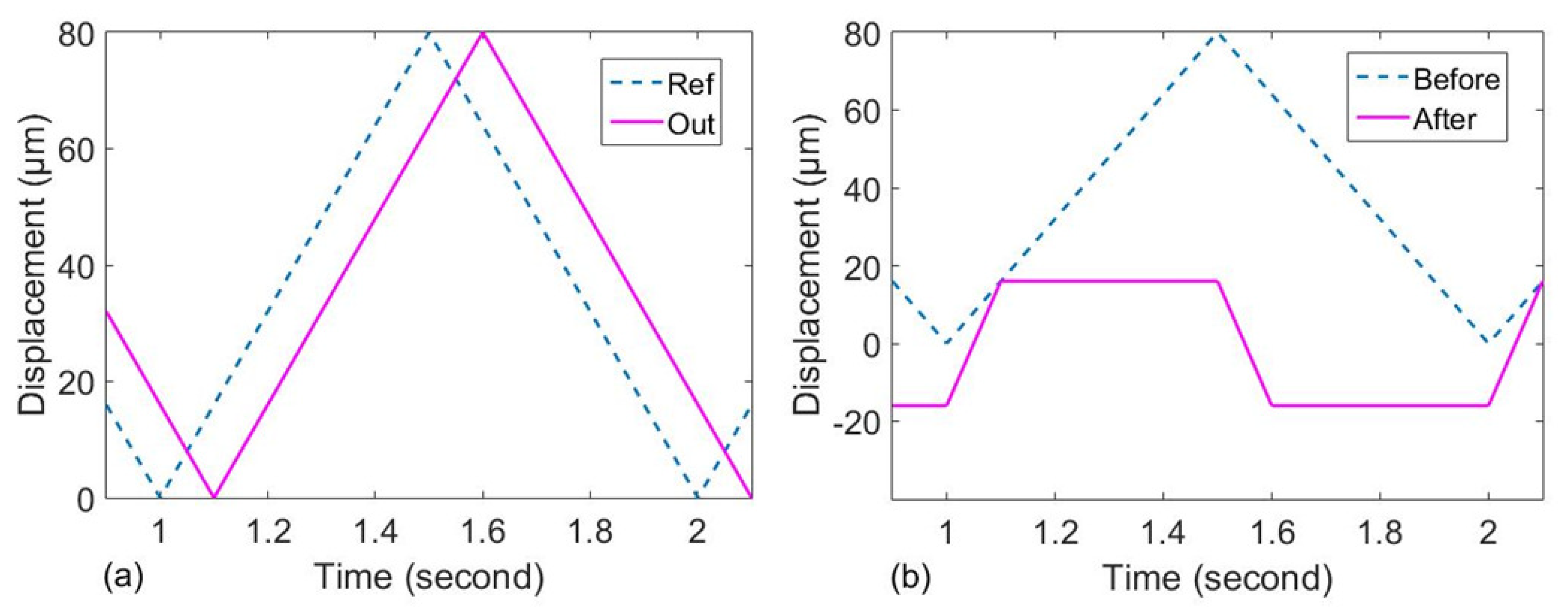
5. Experimental Tests

The whole experimental system is displayed in Figure 9. Aluminum alloy 7075 is selected to fabricate the designed device. Two piezoelectric actuators (P-887.91N, PI and PSt150/10/60 VS15, CoreMorrow) with a three-channel voltage amplifier (E01.B3, CoreMorrow) are used to actuate the compliant 2-DOF ejector pin mechanism. The capacitive displacement sensors (NS-DCS10L-400, SYMC) and fiber-optic displacement sensor (MTI-2100, MTI) are utilized to measure the precision displacement of the device. The open-loop control of this device is achieved by using the dSPACE rapid prototyping simulating system (DS-1007, dSPACE). In order to avoid the external vibration from all kinds of interference, all instruments are placed on the vibration isolation stage (WN01AL, Winner Optics).

5.1. Open-Loop Test

First, the open-loop static properties of the designed device are characterized. A sinusoidal voltage signal with a frequency of 1 Hz ranging from 0 to 10 V is applied to two piezoelectric actuators in turn, resulting in response motion along the driving direction and parasitic movement in the other directions, as shown in Figure 10a,b. It shows that the stroke of the output end can reach 80 μ m in the x-direction and 120 μ m in the y-direction. No matter which piezoelectric actuator is driven, the parasitic motion in the other direction is no more than 0.5%. In short, all the coupling motions of the device are within a reasonable range, and the decoupling performance of the designed mechanism is excellent. Therefore, the influence of parasitic motion on the accuracy of the device cannot be considered. However, due to the hysteresis effect of the piezoelectric actuator, the driving voltage and the output displacement are nonlinear, as shown in Figure 10c, which greatly reduces the positioning accuracy of the system.

5.2. Trajectory Tracking Test

In order to compensate for the inherent hysteresis nonlinearity of the piezoelectric actuator and improve the accuracy of the device, the controller designed in Section 4 of this paper is applied to a series of trajectory tracking experiments. The tracking results of the x-axis and y-axis are highly similar. In order to avoid repeated displays, only the tracking results of the y-axis are shown in Figure 11. As shown in Figure 11a, a sinusoidal signal with a frequency of 10 Hz and a range of 0–95 μ m is adopted as an ideal signal on the y-axis. The error between the actual output and the desired trajectory is ±0.5 μ m. The tracking errors of sinusoidal signals with frequencies of 20 Hz (in Figure 11b) and 30 Hz (in Figure 11c) are ±1.0 μ m and ±1.5 μ m, respectively. The tracking errors of sinusoidal signals with frequencies of 20 Hz and 30 Hz are ±1.0 μ m and ±1.5 μ m, respectively. All errors are within ±1.5% of the working stroke, which proves the perfect tracking performance of the designed device and the effectiveness of the designed controller. However, as shown in Figure 11d, when tracking a signal with higher frequency, the tracking error will increase, indicating that a more advanced control algorithm needs to be further developed in the future.

6. Conclusions

In this paper, a novel compliant 2-DOF ejector pin mechanism for the mini-LED chip mass transfer is proposed, to overcome the shortcomings of the traditional chip eject transfer method with a mechanical ejector pin. The methods of compliance matrix and Newton are employed for system kinematic modeling and dynamics modeling, respectively. The mechanism static and dynamic analyses were carried out via ANSYS Workbench, and the results of FEA are in good agreement with those of the theoretical calculation, which indicates the effectiveness of the design. Then, an ILC is utilized to control the device with a parameter regulation approach in the frequency domain. Finally, an open-loop test and a trajectory tracking test for the prototype are carried out in detail. These indicate that the working stroke of the mechanism can reach 120 μ m, the natural frequency of the device is 250.85 Hz, the coupling rate is less than ±0.5% and the track tracking errors of 10 Hz, 20 Hz and 30 Hz sinusoidal signals are all within ±1.5%. The experimental results show that the transfer efficiency of the designed mechanism can reach 108K UPH. In summary, the working frequency range is over 100K UPH and reaches 108K UPH with the same displacement and accuracy as the traditional mini-LED mass transfer method, such that the effectiveness of the proposed compliant mechanism is proved.
In future work, higher frequency, larger stroke, higher precision devices and more intelligent control algorithms will be developed and be applied to the direct transfer of mini-LEDs. Moreover, the practical processes of mini-LED mass transfer will be carried out to verify the effectiveness of the proposed device.

Author Contributions

Conceptualization, H.T. and Z.L. (Zhihang Lin); methodology, H.L.; software, C.H.; validation, C.H.and S.S., Z.L. (Zhishen Liao) and C.L.; formal analysis, H.L.; investigation, H.L. and S.S.; resources, H.L. and C.H.; data curation, H.L. and C.H.; writing—original draft preparation, Z.L. (Zhishen Liao), H.L. and C.H.; writing—review and editing, H.L., C.H. and H.T.; visualization, H.T.; supervision, Z.L. (Zhihang Lin); project administration, Z.L. (Zhihang Lin) and H.L.; funding acquisition, H.T. All authors have read and agreed to the published version of the manuscript.

Funding

This research was funded by the Natural Science Foundation of China under Grant 51975132, Grant U20A6004, and in part by the Guangdong Programs for Science and Technology under Grant 2019A1515011896.

Institutional Review Board Statement

Not applicable.

Informed Consent Statement

Not applicable.

Data Availability Statement

Not applicable.

Conflicts of Interest

The authors declare no conflict of interest.

References

  1. Virey, E.H.; Baron, N. 45-1: Status and Prospects of MicroLED Displays. SID Symp. 2018, 49, 593–596. [Google Scholar] [CrossRef]
  2. Kamarei, Z.B.N. Analysis for science librarians of the 2014 nobel prize in physics: Invention of efficient blue-light-emitting diodes. Sci. Technol. Libr. 2015, 34, 19–31. [Google Scholar] [CrossRef]
  3. Wang, C.T.; Yang, C.S.; Guo, Q. Liquid Crystal Optics and Physics: Recent Advances and Prospects. Crystals 2019, 9, 670. [Google Scholar] [CrossRef] [Green Version]
  4. Zhang, S.; Gong, Z.; McKendry, J.J.D.; Watson, S.; Cogman, A.; Xie, E.; Tian, P.; Gu, E.; Chen, Z.; Zhang, G.; et al. CMOS-Controlled Color-Tunable Smart Display. IEEE Photonics J. 2012, 4, 1639–1646. [Google Scholar] [CrossRef] [Green Version]
  5. Fan, Z.Y.; Lin, J.Y.; Jiang, H.X. 45-1: III-nitride micro-emitter arrays: Development and applications. J. Phys. D Appl. Phys. 2008, 41, 094001. [Google Scholar] [CrossRef]
  6. Chen, H.; Tan, G.; Wu, S.-T. Ambient Contrast Ratio of LCDs and OLED Displays. Opt. Express 2017, 25, 33643. [Google Scholar] [CrossRef]
  7. Gou, F.; Hsiang, E.L.; Tan, G.; Lan, Y.F.; Tsai, C.Y.; Wu, S.T. Tripling the Optical Efficiency of Color-Converted Micro-LED Displays with Funnel-Tube Array. Crystals 2019, 9, 39. [Google Scholar] [CrossRef] [Green Version]
  8. Li, J.; Luo, B.; Liu, Z. Micro-LED Mass Transfer Technologies. In Proceedings of the 2020 21st International Conference on Electronic Packaging Technology (ICEPT), Guangzhou, China, 12–15 August 2020; Volume 2018, pp. 2020–2022. [Google Scholar] [CrossRef]
  9. Templier, F.; Hsiang, E.L.; Tan, G.; Lan, Y.F.; Tsai, C.Y.; Wu, S.T. GaN-based emissive microdisplays: A very promising technology for compact, ultra-high brightness display systems. J. Soc. Inf. Disp. 2016, 24, 669–675. [Google Scholar] [CrossRef]
  10. Gou, F.; Hsiang, E.-L.; Tan, G.; Chou, P.-T.; Li, Y.-L.; Lan, Y.-F.; Wu, S.-T. Angular Color Shift of Micro-LED Displays. Opt. Express 2019, 27, 593–596. [Google Scholar] [CrossRef]
  11. Liao, Z.; Lin, Y.; Bai, H.; Zhu, Z.; Zhang, P.; Tang, H. A New Flexure-Based Parallel Laser Deflection Device for MicroLED Repair. In Proceedings of the 2020 21st International Conference on Electronic Packaging Technology (ICEPT), Guangzhou, China, 12–15 August 2020; pp. 2–6. [Google Scholar] [CrossRef]
  12. Xiao, J.; Zheng, F.; Fei, J.; Li, J.; Liu, Q.; Huo, W.; Zhuang, J.; Mei, W.; Zhang, S. Electrostatic Discharge Protection of MiniLED Backlight Units on Glass. Energy Rep. 2021, 7, 276–282. [Google Scholar] [CrossRef]
  13. Lu, H.; Guo, W.; Su, C.; Li, X.; Lu, Y.; Chen, Z.; Zhu, L. Optimization on Adhesive Stamp Mass-Transfer of Micro-LEDs with Support Vector Machine Model. IEEE J. Electron Devices Soc. 2020, 8, 554–558. [Google Scholar] [CrossRef]
  14. Bower, C.A.; Meitl, M.; Kneeburg, D. Micro-Transfer-Printing: Heterogeneous Integration of Microscale Semiconductor Devices Using Elastomer Stamps. Proc. IEEE Sens. 2014, 49, 2111–2113. [Google Scholar] [CrossRef]
  15. Meitl, M.; Radauscher, E.; Bonafede, S.; Gomez, D.; Moore, T.; Prevatte, C.; Raymond, B.; Fisher, B.; Ghosal, K.; Fecioru, A. Invited paper: Passive matrix displays with transfer-printed microscale inorganic LEDs. SID Symp. Dig. Tech. Pap. 2016, 47, 743–746. [Google Scholar] [CrossRef]
  16. Bai, H.; Tang, H.; Feng, Z.; Liao, Z.; Gao, J.; Liu, Q.; Chen, X. Development of a Novel Intelligent Adjustable Vision Algorithm for LED Chip Repairing. IEEE Trans. Ind. Electron. 2022, 69, 7109–7119. [Google Scholar] [CrossRef]
  17. Xia, J.; Dong, X.; Yao, Z.; Sheng, C.; Li, Z.; Cao, X.; Wang, C.; Duan, L. Development of High-Yield Laser Lift-off Process for Micro Led Display. Dig. Tech. Pap.—SID Int. Symp. 2020, 51, 1312–1314. [Google Scholar] [CrossRef]
  18. Cho, S.; Lee, D.; Kwon, S. Fluidic self-assembly transfer technology for micro-led display. In Proceedings of the 2019 20th International Conference on Solid-State Sensors, Actuators and Microsystems & Eurosensors XXXIII (TRANSDUCERS & EUROSENSORS XXXIII), Berlin, Germany, 23–27 June 2019; pp. 402–404. [Google Scholar] [CrossRef]
  19. Hiraki, K. Wafer Direct Technology for Mini LED Flip Attachment. J. Phys. Conf. Ser. 2021, 2065, 012015. [Google Scholar] [CrossRef]
  20. Wu, T.; Sher, C.W.; Lin, Y.; Lee, C.F.; Liang, S.; Lu, Y.; Chen, S.W.H.; Guo, W.; Kuo, H.C.; Chen, Z. Mini-LED and Micro-LED: Promising Candidates for the next Generation Display Technology. Appl. Sci. 2018, 8, 1557. [Google Scholar] [CrossRef] [Green Version]
  21. Sun, Y.; Zhang, M. Highly Transparent, Ultra-Thin Flexible, Full-Color Mini-LED Display with Indium–Gallium–Zinc Oxide Thin-Film Transistor Substrate. J. Soc. Inf. Disp. 2020, 12, 926–935. [Google Scholar] [CrossRef]
  22. Tang, H.; He, S.; Zhu, Z.; Gao, J.; Zhang, L.; Cui, C.; Chen, X. A Monolithic Force Sensing Integrated Flexure Bonder Dedicated to Flip-Chip Active Soft-Landing Interconnection. IEEE/ASME Trans. Mech. 2021, 26, 323–334. [Google Scholar] [CrossRef]
  23. Li, J.; Tang, H.; Zhu, Z.; He, S.; Gao, J.; He, Y.; Chen, X. Hybrid Position/Force Fully Closed-Loop Control of a Flip-Chip Soft-Landing Bonding System. IEEE Trans. Ind. Electron. 2022, 69, 9235–9245. [Google Scholar] [CrossRef]
  24. He, S.; Tang, H.; Zhu, Z.; Zhang, P.; Xu, Y.; Chen, X. A Novel Flexure Piezomotor with Minimized Backward and Nonlinear Motion Effect. IEEE Trans. Ind. Electron. 2022, 69, 652–662. [Google Scholar] [CrossRef]
  25. Wang, F.; Zhao, X.; Huo, Z.; Shi, B.; Liang, C.; Tian, Y.; Zhang, D. A 2-DOF Nano-Positioning Scanner with Novel Compound Decoupling-Guiding Mechanism. Mech. Mach. Theory 2021, 155, 104066. [Google Scholar] [CrossRef]
  26. Tran, N.T.; Dao, T.; Nguyen-Trang, T.; Ha, C. Prediction of Fatigue Life for a New 2-DOF Compliant Mechanism by Clustering-Based ANFIS Approach. Math. Probl. Eng. 2021, 2021, 6672811. [Google Scholar] [CrossRef]
  27. Huang, S. Design and Computational Optimization of a Flexure- Based XY Positioning Platform Using FEA-Based Response Surface Methodology. Int. J. Precis. Eng. Manuf. 2016, 17, 1035–1048. [Google Scholar] [CrossRef]
  28. Li, H.; Tang, H.; Li, J.; Chen, X. Design, Fabrication, and Testing of a 3-DOF Piezo Fast Tool Servo for Microstructure Machining. Precis. Eng. 2021, 72, 756–768. [Google Scholar] [CrossRef]
  29. An, D.; Yang, Y.; Xu, Y.; Shao, M.; Shi, J.; Yue, G. Compensation of Hysteresis in the Piezoelectric Nanopositioning Stage under Reciprocating Linear Voltage Based on a Mark-Segmented PI Model. Micromachines 2020, 11, 9. [Google Scholar] [CrossRef] [Green Version]
  30. Arimoto, S.; Kawamura, S.; Miyazaki, F.; Tamaki, S. Learning control theory for dynamical systems. In Proceedings of the 24th IEEE Conference on Decision and Control, Fort Lauderdale, FL, USA, 11–13 December 1985; pp. 1375–1380. [Google Scholar] [CrossRef]
  31. Wang, D.; Ye, Y.; Zhang, B. Practical Iterative Learning Control with Frequency Domain Design and Sampled Data Implementation; Springer: Singapore, 2014; ISBN 978-981-4585-59-0. [Google Scholar]
  32. Meng, D.; Wu, Y. A Survey on Distributed Iterative Learning Control for Transient Formation. Control. Theory Technol. 2021, 19, 295–297. [Google Scholar] [CrossRef]
  33. Elci, H.; Longman, R.W.; Phan, M.Q.; Juang, J.N.; Ugoletti, R. Simple Learning Control Made Practical by Zero-Phase Filtering: Applications to Robotics. IEEE Trans. Circuits Syst. I Fundam. Theory Appl. 2002, 49, 753–767. [Google Scholar] [CrossRef]
Figure 1. Conventional chip ejection transfer process with a mechanical ejector pin. (a) The target chip is moved below the ejector pin. (b) The ejector pin pushes the epitaxial film downward. (c) The target chip is contacted and fixed on the substrate. (d) The stage moves and the next chip is transferred.
Applsci 12 05423 g001
Figure 2. Compliant 2-DOF ejector pin mechanism for the mass transfer of robotic mini-LED chips. (a) Schematic diagram of the designed mini-LED transfer device. (b) Three-dimensional diagram of the designed device. (c) Schematic diagram of continuous chip ejection.
Applsci 12 05423 g002
Figure 3. Schematic of the designed compliant mechanism. (a) The designed compliant mechanism. (b) The leaf flexure. (c) The L-shaped flexure.
Applsci 12 05423 g003
Figure 4. The schematic diagram of the dynamic model of the mechanism.
Applsci 12 05423 g004
Figure 5. The FEA results. (a) The first mode: 250.85 Hz, x-axis direction. (b) The second mode: 256.76 Hz, y-axis direction. (c) The third mode: 494.84 Hz. (d) The fourth mode: 646.99 Hz, z-axis direction. (e) The third mode: 919.15 Hz. (f) The third mode: 1876 Hz.
Applsci 12 05423 g005
Figure 6. Nyquist plot of γ · e j · ω · t s · G ( e j · ω · t s ) with different γ .
Applsci 12 05423 g006
Figure 7. Comparison results. (a) Reference and open-loop input. (b) Tracking error before and after adding compensation in the initial state of the ILC.
Applsci 12 05423 g007
Figure 8. The diagram of the control scheme in this article.
Applsci 12 05423 g008
Figure 9. Experimental setup: (1) voltage amplifier; (2) fiber-optic displacement sensor; (3) dSPACE control system; (4) capacitive displacement sensor; (5) designed compliant 2-DOF ejector pin mechanism; (6) vibration isolation stage; (7) host display; (8) fixture; (9) piezoelectric actuator; (10) capacitance displacement sensor probe; (11) fiber-optic displacement sensor probe; (12) compliant mechanism; and (13) eject pin.
Applsci 12 05423 g009
Figure 10. Open-loop test. (a) Driving along the x-axis. (b) Driving along the y-axis. (c) The hysteresis effect of the piezoelectric actuator.
Applsci 12 05423 g010
Figure 11. Trajectory tracking results. (a) Sinusoidal signal with a frequency of 10 Hz. (b) Sinusoidal signal with a frequency of 20 Hz. (c) Sinusoidal signal with a frequency of 30 Hz. (d) Trajectory tracking errors.
Applsci 12 05423 g011
Table 1. Material and Structure Parameters.
Material ParametersStructural Parameters (mm)
E
(GPa)
σ y
(MPa)
μ ρ
(kg/m 3 )
lbt l 1 l 2 l 3
71.75030.33281029.581958520
Table 2. Comparisons between FEA and the theoretical model.
ComplianceFrequency
C δ x , F x o u t ( μ m/N) C δ y , F y o u t ( μ m/N) f x (Hz) f y (Hz)
Theoretical14.5114.51267.16267.16
FEA14.7415.22250.85256.76
Error1.59%4.89%6.10%3.89%
Publisher’s Note: MDPI stays neutral with regard to jurisdictional claims in published maps and institutional affiliations.

