Article

Characterization of a New Low Temperature Encapsulation Method with Ethylene-Vinyl Acetate under UV Irradiation for Perovskite Solar Cells

by
Luis Ocaña
1,2,*,
Carlos Montes
1,2,
Sara González-Pérez
3,
Benjamín González-Díaz
2 and
Elena Llarena
1
1
Instituto Tecnológico y de Energías Renovables, S. A. (ITER), 38600 Santa Cruz de Tenerife, Spain
2
Departamento de Ingeniería Industrial, Escuela Superior de Ingeniería y Tecnología, Universidad de La Laguna (ULL), 38200 Santa Cruz de Tenerife, Spain
3
Departamento de Didácticas Específicas, Universidad de La Laguna (ULL), 38200 Santa Cruz de Tenerife, Spain
*
Author to whom correspondence should be addressed.
Appl. Sci. 2022, 12(10), 5228; https://doi.org/10.3390/app12105228
Submission received: 21 April 2022 / Revised: 12 May 2022 / Accepted: 19 May 2022 / Published: 21 May 2022
(This article belongs to the Topic Perovskites for Energy Applications)

Abstract

:
In this work, the performance of a new ethylene-vinyl acetate-based low temperature encapsulation method, conceived to protect perovskite samples from UV irradiation in ambient conditions, has been analyzed. To this purpose, perovskite samples consisting of a set of MAPbI3 (CH3NH3PbI3) films and MAPbI3 with an ETL layer were deposited over glass substrates by spin-coating techniques and encapsulated using the new method. The samples were subjected to an UV lamp or to full solar irradiation in ambient conditions, with a relative humidity of 60–80%. Microscope imaging, spectroscopic ellipsometry and Fourier-transform infrared spectroscopy (FTIR) techniques were applied to analyze the samples. The obtained results indicate UV energy is responsible for the degradation of the perovskite layer. Thus, the cut-UV characteristics of the EVA encapsulate acts as an efficient barrier, allowing the laminated samples to remain stable above 350 h under full solar irradiation compared with non-encapsulated samples. In addition, the FTIR results reveal perovskite degradation caused by UV light. To extend the study to encompass whole PSCs, simulations were carried out using the software SCAPS-1D, where the non-encapsulated devices present a short-circuit current reduction after exposure to UV irradiation, while the encapsulated ones maintained their efficiency.

1. Introduction

Solar cells based on perovskite structures (PSCs) have registered a significant power conversion efficiency (PCE) increase in recent years, achieving a record of 25.7% for non-stabilized PSCs, 29.8% for perovskite/Si tandem (monolithic) [1] and 17.9% for perovskite modules [2]. These efficiencies have demonstrated PSCs as a promising candidate capable to compete in a silicon dominated solar cells market.
The degradation mechanisms for PSCs are mainly caused by exposure to moisture, oxygen, heat, UV light, light soaking, mechanical stress and reverse bias [3,4]. From all these, moisture is considered the most determining factor in the degradation of the MAPbI3 layer [4], mainly due to the hygroscopic nature of the amine salt [3,5]. Additionally, the composition of perovskite can be affected by defects, which can significantly change its properties depending on the radiation and temperature [6,7].
However, the stability of the achieved PCE remains a key issue to be solved in order to assure the lifetime and the durability of these kinds of technologies. Several research lines have been addressed to enhance stability, such as introducing variations on the structure composition of the perovskites [8,9,10,11,12], the inclusion of new layers, such as hydrophobic films [13,14,15,16], the replacement of the metallic electrode by carbon or a transparent conductive oxide to avoid problems with the hole transporter layer [17,18,19,20] or using encapsulation methods in order to isolate and protect the device from environmental agents [4,21,22,23].

1.1. Degradation Mechanisms

The degradation process in the MAPbI3 layer occurs when the methylamine group (MAI) is lost via sublimation and PbI2 is formed [3,24], according to Equations (1) and (2). MAPbI3−xClx and MAPbI3 present a similar moisture assisted degradation where methylamine group is lost via sublimation and PbI2 is formed. The highly hydrophilic property of perovskite allows the absorption of the water from the surrounding environment [3]. As a result, the perovskite layer, which is originally of a brownish color, gradually turns yellow [4]. Oxygen and ultraviolet radiation can further affect the stability of PSCs, as can be seen in Equations (3) and (4) [3,8], albeit to a lesser extent than humidity [25].
MAPbI3 is one of the most common forms in which the perovskite layer is manufactured. The degradation equations of the perovskite layer under moisture, oxygen and UV light are depicted below [25]:
MAPb I 3 ( s )   +   H 2 O     MAI   ( aq . )   +   Pb I 2 ( s )
MAI ( aq . )     MA ( aq . )   +   HI ( aq . )
4 HI ( aq . )   +   O 2     2 I 2 ( s )   +   H 2 O
2 HI ( aq . )   +   h ʋ     H 2 ( g )   +   2 I 2 ( s )
Additionally, under UV irradiation, the presence of oxygen and water molecules at the heterojunction between the electron transport layer (ETL) and the perovskite layer results in a redox reaction within their comprised elements, which leads to the decomposition of the perovskite, reducing the performance of the PSCs [8,26]. The characteristics of the ETL are related to the optoelectronic performance of the device. The long-term stability of the device is influenced by trivalent Ti ions, and oxygen vacancies are generated by the irradiation of TiO2 valence band electrons under ultraviolet (UV) light. The oxygen vacancies on the surface of TiO2 are able to adsorb oxygen and water molecules, accelerating the degradation of the perovskite layer [8].

1.2. Encapsulation of the Perovskites

The parameters that need to be controlled for any encapsulation material are the elastic modulus, the impermeability against water, the volume resistivity and the protection against UV irradiation.
In mechanical terms, the perovskite layer has a thermal expansion coefficient ten times higher than the glass substrate or than the transparent conductive oxide it sits upon, so the mechanical stresses caused by temperature changes results in delamination processes between these layers, accelerating their decomposition [27,28]. Therefore, it is important to choose an encapsulation material that has a low elastic module. Furthermore, as has been described previously, moisture quickly attacks the perovskite structure, so the encapsulation material of choice must have a low rate of water vapor transmission (WVTR) [4]. Additionally, PCSs have high voltages. These voltages increase considerably when they are used to produce modules. High voltage also activates degradation processes on the PCSs, producing chemical reactions that generate harmful by-products. Therefore, it is important to select an encapsulation material that has a high volume resistivity [4]. Finally, as has been described previously, UV irradiation starts degradation processes on the PCSs, which is triggered by photo-degradation [29]. Therefore, it is important to select an encapsulation material that prevents the passage of UV irradiation.
The first encapsulates tried were based on the use of thin layers, formed by either Al2O3 or inorganic/organic multilayers, applied together with an adhesive. This kind of encapsulation presented many advantages, such as having low deposition temperature requirements that prevented the evaporation of organic volatile compounds, and its low WVTR, below 10–5 (g/m2/day) [30,31]. However, the high elastic modulus caused delamination after several thermal cycles. Currently, these encapsulants are still in use with flexible devices [32]. These encapsulates must take special care in sealing the edges, since the humidity that penetrates through the sides of the encapsulation is sufficient to initiate degradation [33,34]. Some of these encapsulants are Teflon [35], Adamantane Nanocomposite [22], UV curable fluoropolymers [36], Al2O3/pv3D3 [32] or organosilicates [37].
Nowadays, the encapsulation of PSCs is based on designs that are used in CIGS and CdTe photovoltaic cells, since these cells have stability issues similar to those of PSCs, mainly in terms of humidity [38]. To solve these issues, glass is used as a cover material together with polymer layers and sealant materials applied at the edges [39]. The most common materials used for encapsulation are epoxy resin [40,41], ethylene-vinyl acetate (EVA) [42,43], surlyn [41,42,43,44,45], ethylene-vinyl-alcohol (EVOH) [46], poly (ethylene terephthalate) (PET) [41,47], poluisobutylene (PBI) [48], poly methyl methacrylate (PMMA) [41], UV-curable glue [49] and polyolefilm [43]. From all of these materials, EVA is the most widely used encapsulant in the photovoltaic industry, due to its low cost, high light transmittance (93%; freestanding EVA) and low curing temperature (140 °C) [4].

1.3. Aim and Scope

In this work, a new low-temperature encapsulation method, based on the use of EVA, has been developed to protect PSCs from UV irradiation and environment humidity. In order to analyze it, a research procedure has been carried out in three stages. The first one consists of the fabrication of four sets of samples: one composed of non encapsulated perovskite, one composed of non-encapsulated perovskite and ETL, one composed of encapsulated perovskite and one composed of encapsulated perovskite and ETL. In the second stage, all the samples were exposed to UV irradiation and full solar irradiation in humid environments. In the third and last stage, the samples were characterized in order to infer their degree of degradation.

2. Materials and Methods

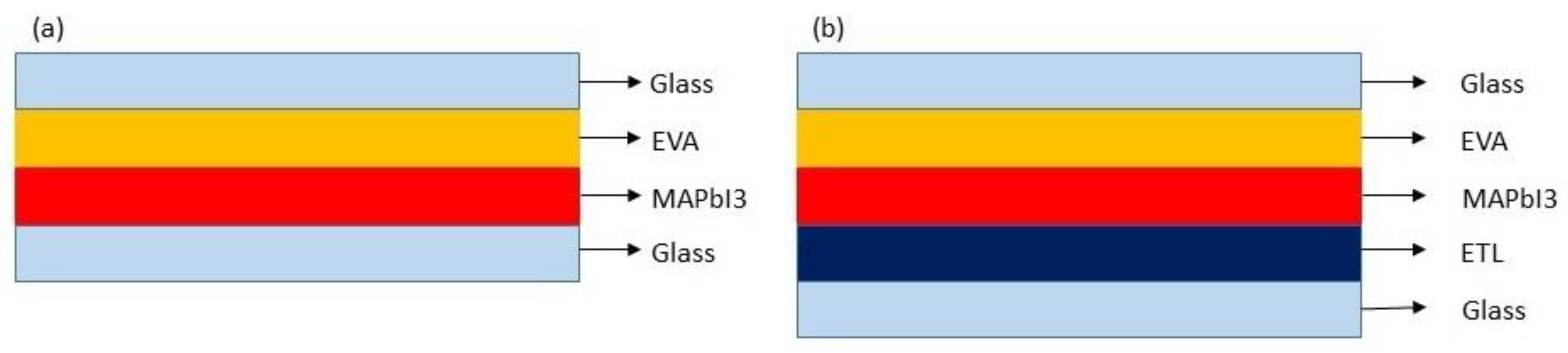
2.1. Sample Preparation

All the fabrication processes were carried out inside an ISO7 cleanroom, operating at 23 °C and at a relative humidity (RH) from 30% to 40%. Due to the relevance and influence of the RH [50] and the temperature [51] on the fabrication procedures, these parameters were constantly monitored during fabrication steps.
Then, 25 mm × 25 mm and 2 mm thick soda line silica glass substrates were cleaned sequentially by ultrasonication in a 2% soap solution, deionized water, acetone and 2-propanol and dried with nitrogen [52]. After that, an ultraviolet–ozone (UVO) treatment was used to remove the contaminants from the surface of the samples in order to facilitate the interface between the substrate and the electron transport layer [53,54]

2.2. Synthesis and Sample Fabrication

The synthesis of the perovskite precursor solution was performed by stirring PbI2 (Lead (II) iodide, Sigma Aldrich 211168, St. Louis, MO, USA) and CH3NH3I (MAI 98%, TCI M2556) at a molar ratio of 1:1, using a mixture of N,N-Dimethylformamide (DMF 99.8%, Sigma Aldrich 227056) and Dimethyl sulfoxide (DMSO 99.9%, Sigma Aldrich 276855) with a 9:1 (v/v) ratio at 75 °C for 50 min and at room temperature overnight [55]. The obtained solution was passed through a 0.22 μm Polytetrafluoroethylene (PTFE) filter prior to deposition [56]. A volume of 100 μL of perovskite precursor solution was dispensed on top of glass substrates and then was subjected to a spin rate of 5000 rpm for 30 s. During the spinning, a 3:1 volume ratio of a non-polar solvent (chlorobenzene) was dropped over the substrate, achieving a layer thickness of 300 nm [55], and the RH inside the chamber was maintained between 8–10%, with a constant flow of clean dry air (CDA) [55]. Finally, the sample was annealed at 100 °C for 10 min inside a furnace to evaporate any residual solvent and to promote crystallization [57]. Samples were stored in a vacuum desiccator to avoid degradation [58,59].
The synthesis of the electron transport layer (ETL) was performed by dropwise adding a solution of 175 μL of Titanium (IV) isopropoxide (TTIP 97%, Sigma Aldrich 205273) in 1.25 mL of EtOH (Ethanol 99.9%, Merck 1.00983.2500, Kenilworth, NJ, USA) into a solution of 17.5 μL of 2 M HCl (Hydrochloric acid 37%, Labkem CHAC-0AA-2K5, Dukinfield, UK) in 1.25 mL of EtOH [60]. A 0.22 μm PTFE filter was used to obtain the solution. Finally, the precursor solution (150 μL) was dispensed on top of glass substrates, and then the samples were spin-coated at 2000 rpm for 60 s. To obtain a thickness layer of 80 nm, a double ETL was deposited using the spin-coating technique. After the deposition, the first layer was heated to 150 °C for 30 min, and the second layer was spin-coated and heated to 500 °C for 60 min.

2.3. Encapsulation of the Samples

The encapsulating process was performed by using temperature and pressure lamination techniques [61], in which a sheet of commercial EVA (Encapsolar PC-135 A, from Stevens Urethane, Easthampton, MA, USA) was placed between the perovskite layer and the cover soda lime silica glass. Because the assembled sandwich could lose its integrity during the thermal process, a thick steel plate was used to apply uniform pressure. In order to take into account the steel thermal inertia, the samples were cured at 100 °C for 165 min and cooled down for 125 min before removing the steel plate.
Two kinds of samples were encapsulated. The architecture of the samples type (a) consists of a perovskite thin film, deposited over a glass substrate and encapsulated with a layer of EVA and yet another glass. Type (b) also adds an ETL layer between glass and perovskite (Figure 1).

2.4. Characterization

A digital microscope (U500X by Unimake, Campo Mourão, Brazil) with a focus range from 15 mm to 40 mm and a magnification range of 50×–500× was used during the degradation processes to analyze the samples.
Ellipsometry measurements were carried out using the spectroscopic ellipsometer M-2000 from J. A. Woollam Co., Inc. (Lincoln, NE, USA), with a spectral range from 245 nm to 1000 nm, a laser light source (FLS) and a xenon arc lamp, with a spot of 500 µm. CompleteEASE software, from the same manufacturer, was used to analyze the optical properties of the layers, obtaining the refractive index (n) and the extinction coefficient (k), as well as the thickness of the layers from the reflectance measurements. On the other hand, the mobility range of the emitter unit and receiver unit, from 45° to 90°, allow transmittance measurements, which allows calculating the absorbance curves and obtain the bandgap [62,63].
Fourier-transform infrared spectroscopy was carried out using an IFS 66/S Bruker, (Bruker, Hanau, Germany) equipment with full spectral range coverage from the very far infrared (<5 cm−1) up to the vacuum UV (>55,000 cm−1), and a spectral resolving power of 100,000:1 or <0.1 cm−1 spectral resolution and peak to peak noise of less than 10−5 AU achieved within 1 min and 4 cm−1 spectral resolution. Spectra were used to establish the MAPbI3 characteristic functional groups by localizing their indicator peaks and to observe their evolution as the degradation processes took place.

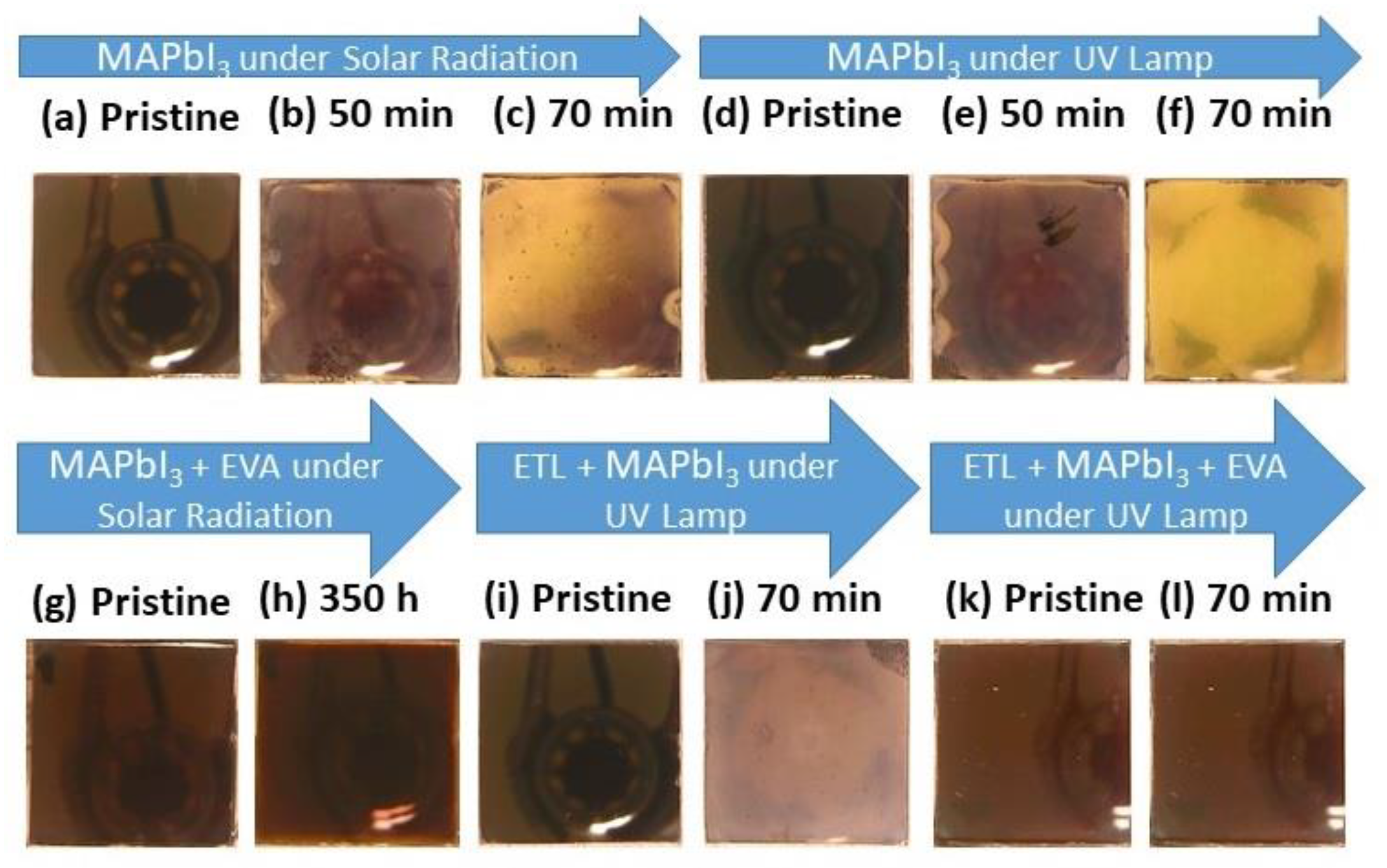
2.5. Degradation of the Samples

To evaluate the light induced degradation of the perovskite films due to UV irradiation, two different setups were used. First setup consisted in a UV Lamp of 24 W (365–395 nm), placed at 90° over the samples. In the second setup, the samples were placed outdoors at the Technological and Renewable Energy Institute in Canary Islands (28.071402518377827, −16.514065045493652) on a support inclined at 30 degrees above the horizontal and oriented to the south in order to receive full solar irradiation.
To study the evolution of the degradation process due to UV irradiation, the encapsulated and non-encapsulated MAPbI3 samples were exposed to both irradiation sources, varying the irradiation time from 50 min to 70 min. The total irradiation supplied to the samples was 34,157 W/m2 (50 min) and 47,820 W/m2 (70 min) for the UV lamp and 34,872 W/m2 (50 min) and 50,431 W/m2 (70 min) for the full solar exposure. Additionally, the encapsulated MAPbI3 samples were further exposed to full solar irradiation (6051 kW/m2, 350 h) in order to analyze their stability over a longer period of irradiation time. Finally, to assess the influence of the ETL film during the UV degradation process, the encapsulated and non-encapsulated MAPbI3 with ETL samples were exposed to 47,820 W/m2 (70 min) by using the UV Lamp.

3. Experimental Results

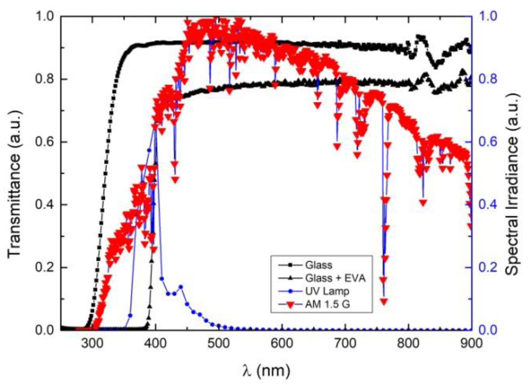
3.1. Transmittance and Visual Analysis

Figure 2 shows a spectral transmittance study performed on the glass and the EVA material used to encapsulate the samples. These data are shown together with the spectrum of the full solar irradiation (AM 1.5 G) and of the UV lamp used in the degradation processes. As is shown, the encapsulant built of glass and EVA acts as an effective UV block agent below 400 nm.
Figure 3 shows the transformation observed on the MAPbI3 and MAPbI3 with ETL samples, encapsulated and non-encapsulated, during the degradation process, starting from their pristine stages (Figure 3a,d,g,i,k). As can be seen, the non-encapsulated MAPbI3 samples show a similar visual degradation when exposed to both full solar irradiation and UV lamp irradiation. The non-encapsulated samples present decoloring into a dull brown color after 50 min of exposure (Figure 3b,e), turning to a yellowish shade after 70 min (Figure 3c,f). These results are attributed to a degradation mechanism triggered by UV irradiation in a humid environment [4,46,64,65,66]. However, the visual appearance of the encapsulated MAPbI3 samples remained stable above 350 h under full solar irradiation (Figure 3g,h). Additionally, although the non-encapsulated samples of MAPbI3, with and without the ETL layer, show a similar degradation, the ones with ETL acquire the characteristic yellowish shade after 70 min of UV irradiation (Figure 3j), indicating that the ETL layer somehow delays the degradation. In addition, the encapsulated MAPbI3 with the ETL layer sample remained stable after 70 min exposure (Figure 3l).

3.2. Spectroscopic Ellipsometer

The spectroscopic ellipsometer was used to obtain the absorbance curves for the produced samples according to their composition.

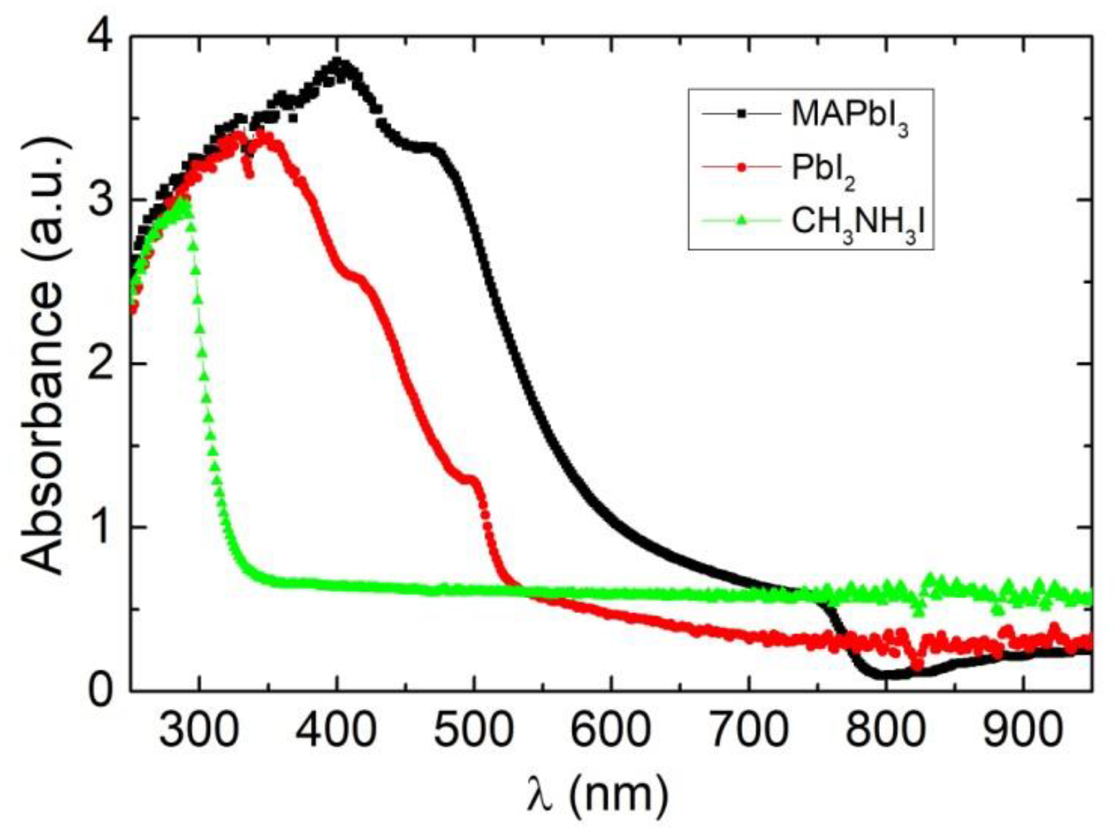
3.2.1. Precursors, Solvents and MAPbI3

According to Equation (1), the decomposition of perovskite results in the appearance of PbI2 and CH3NH3I. Therefore, absorbance curves were performed to fresh deposited layers of MAPbI3, PbI2 and CH3NH3I in order to obtain their characteristic peaks (Figure 4). Thus, the PbI2 absorbance spectrum presents three characteristic peaks, centered in 330 nm, 420 nm and close to 500 nm, while the CH3NH3I only presents absorbance in the UV range of the spectrum, with a peak at 300 nm. The MAPbI3 sample shows broader absorbance bands, in comparison with PbI2, although its characteristic peaks are shifted 50 nm to longer wavelengths. Furthermore, a band gap of 1.6 eV was calculated from the absorbance spectrum of the MAPbI3 sample [62,63].

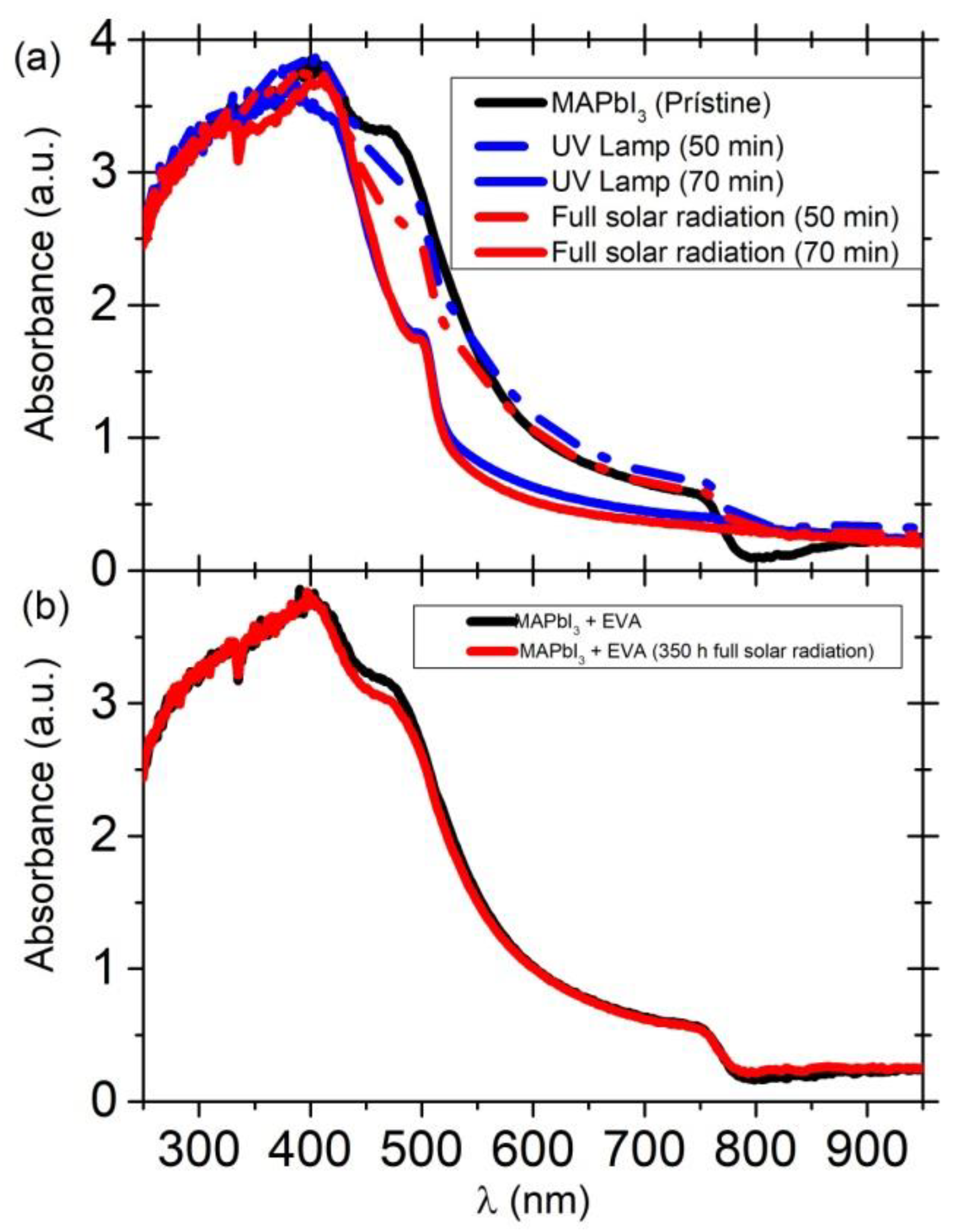
3.2.2. Non-Encapsulated and Encapsulated MAPbI3 Samples

The absorbance measurements were made to the MAPbI3 encapsulated and non-encapsulated samples, before and after subjecting them to the degradation processes.
The absorbance spectra of the encapsulated and non-encapsulated samples after being subjected to full solar irradiation and UV lamp are shown in Figure 5a. As can be seen, the absorbance of the encapsulated and non-encapsulated layers is similar, independently of the light source used. Therefore, the degradation mechanisms involved could be similar under both irradiation methods. In relation to the pristine samples, the absorbance curves of the non-encapsulated MAPbI3 samples show a decrease between 400 nm and 500 nm after 50 min of irradiation. This decrease is extended to 760 nm after 70 min, the moment at which the absorbance curve becomes similar to the PbI2 one. Additionally, the band gap increases from 1.6 to 2.2 eV. Since the degradation experienced by MAPbI3 was the same under both kinds of irradiation sources, it can be deduced that it was caused solely by the UV part of the spectrum [67,68,69].
Furthermore, in order to analyze the effect of the encapsulation on the stability of the MAPbI3 samples, they were exposed to 350 h of full solar irradiation. It must be taken into account that the study of the encapsulated samples should start from 400 nm due to the absorption of the EVA sheet in the UV range. As can be seen, in relation to the pristine samples, the absorption spectra of the exposed samples present only a slight decrease of around 450 nm due to the encapsulation procedure (Figure 5b).

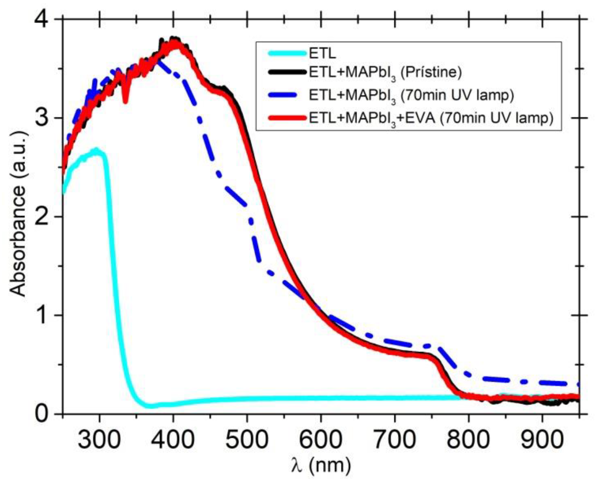
3.2.3. Non-Encapsulated and Encapsulated MAPbI3 with ETL Samples

Absorption curves were determined from non-encapsulated and encapsulated MAPbI3 with ETL samples before and after being subjected to the degradation process. Additionally, an absorption curve was determined by a pristine sample made of ETL deposited on a glass substrate.
If the absorption curves of the pristine samples are compared with the encapsulated and non-encapsulated samples after subjecting them to 70 min of UV irradiation, it can be seen that the non-encapsulated samples show a reduction in the absorbance curve between 400 and 500 nm (see Figure 6). However, the encapsulated ones keep their absorption curve unaltered. In both cases, the calculated band gap remained the same (1.6 eV).
Furthermore, considering only the non-encapsulated samples that went through the degradation process, by comparing Figure 5 and Figure 6, it is possible to infer that the addition of the ETL layer resulted in a reduction in the MAPbI3 degradation, as can be seen at 470 nm (29.68%), at 500 nm (25.35%) and at 750 nm (19.69%). In the same line, non-encapsulated samples without ETL show a similar behavior with a further decrease in the absorption intensity at 470 nm (37.20%), at 500 nm (37.00%) and at 750 nm (28.15%). Therefore, both samples have a similar shift trend, but when the ETL layer is introduced, the absorption intensity peaks show a minor decrease. These results are attributed to the ETL layer effects, which protect the perovskite and EVA layers from degradation by UV irradiation. The ETL layer absorb a fraction of the UV irradiation (from 200 to 350 nm), as shown in Figure 6, therefore reducing the total UV irradiation interacting with the perovskite.

3.3. Fourier-Transform Infrared Spectroscopy (FTIR)

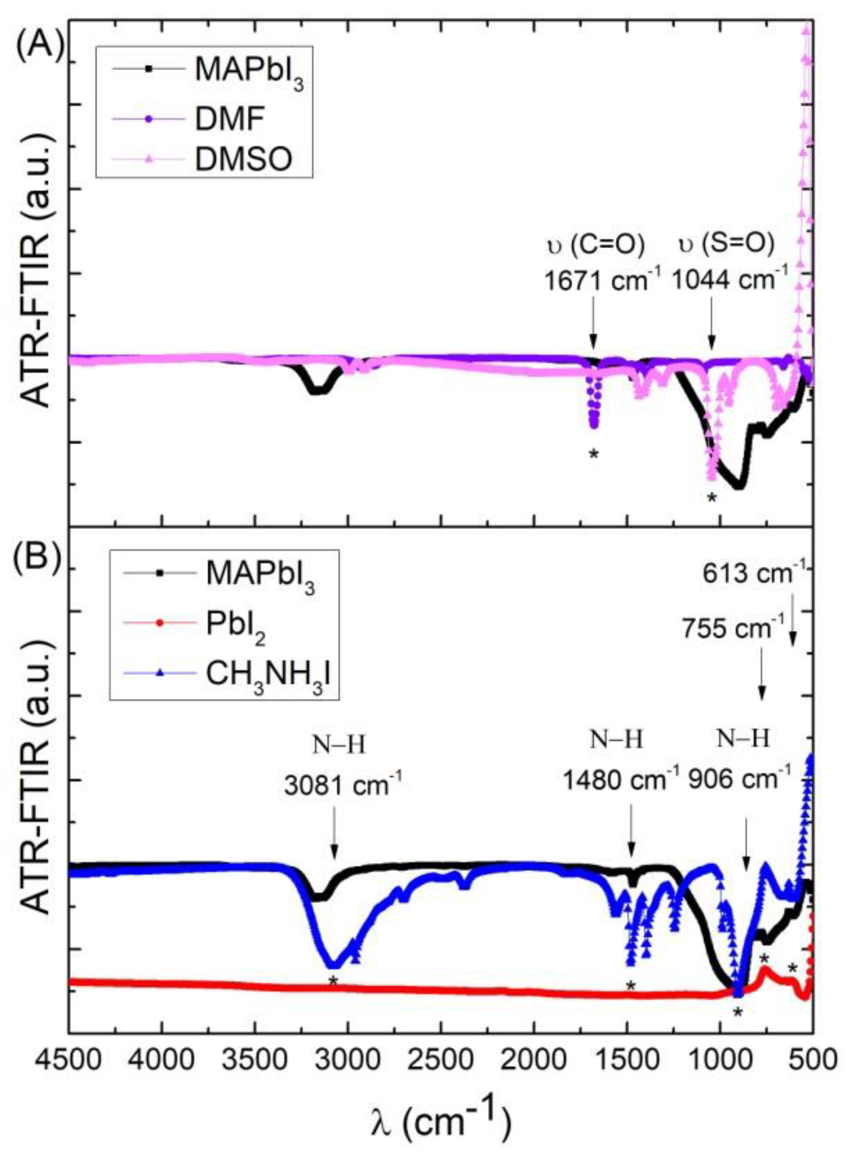
3.3.1. Precursors, Solvents and MAPbI3

PbI2, CH3NH3I as precursor of perovskite and DMF, DMSO as the solvents used for the solution, together with MAPbI3 samples, were analyzed by Fourier-transform infrared spectroscopy in order to compare their characteristic functional groups.
The FTIR spectra for DMF and DMSO solvents (Figure 7A) show that the C=O bond strength are situated at 1671 cm−1 in DMF [70,71], and that the stretching vibration of S=O is located at 1045 cm−1 in DMSO [71,72]. Furthermore, the DMF spectrum shows a symmetrical and asymmetrical C-H bending vibrations related to the two bands located at 1457 cm−1 and 1388 cm−1, respectively [70]. As can be seen, all these bands disappear from the FTIR spectra obtained from the MAPbI3 sample.
The PbI2, CH3NH3I and MAPbI3 FTIR spectra are shown in Figure 7B. The 1480 cm−1 (symmetric NH3+ bend), the 906 cm−1 (NH3+/CH3 rock) and the 3081 cm−1 (N-H stretch) correspond to CH3NH3I [29,73]. The peaks located at 755 cm−1 and 613 cm−1 could be attributed to PbI2 vibration modes [74].
As can be seen, the characteristic peaks identified for the precursors contribute to define the ones seen in the perovskite FTIR spectra.

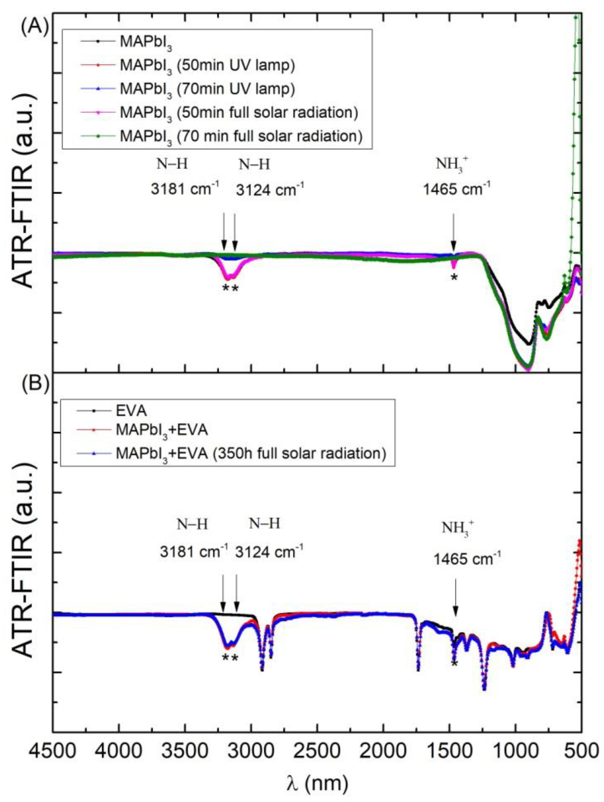
3.3.2. Non-Encapsulated and Encapsulated MAPbI3 Samples

Non-encapsulated and encapsulated MAPbI3 samples were prepared and subjected to the degradation process. Fourier-transform infrared spectroscopy analysis was performed to the samples before (pristine) and after the degradation process.
By comparing the FTIR spectra of the perovskite samples before and after subjecting them to the degradation process, it is possible to observe the existence of vibration modes clearly defined in the pristine perovskite, which disappear after the degradation process takes places. These are at 3181 cm−1 (N-H stretch), 3124 cm−1 (N-H stretch) and 1465 cm−1 (symmetric NH3+ bend) [73]. In fact, having exposed the samples to full solar and UV lamp irradiations, a slight decrease in these peaks happened after 50 min degradation, and they completely disappeared after 70 min degradation, as can be seen in Figure 8A. Since this phenomenon turned out to be the same in both cases of degradation, it is possible to infer that the UV range of the spectra was the agent responsible for said degradation. This hypothesis was also supported by the FTIR spectra performed to the encapsulated samples that were subjected to 350 h of full solar irradiation, where the observed vibration modes remained stable due to the UV-cut properties of the EVA material applied (see Figure 8B).
Finally, it is important to notice that the intermediate complex sensitive to hydration, which lies at 1660 cm−1 [75], was not observed in any of the samples. Therefore, no degradation due to humidity was apparent, despite performing all the tests in ambient conditions.

3.3.3. Non-Encapsulated and Encapsulated MAPbI3-ETL Samples

The degradation of the MAPbI3 layer was also evaluated in terms of its interaction with an ETL layer, due to being exposed to UV irradiation. In Figure 9, a reduction in the characteristic peaks can be observed at 3181 cm−1 (38.71%), at 3124 cm−1 (36.20%) and at 1465 cm−1 (40.79%). The observed intensity reductions in the degraded MAPbI3 samples for these peaks were 73.73%, 72.91% and 69.79%, respectively. This difference suggests that the degradation of the MAPbI3 with ETL samples is lower than that of MAPbI3 ones. Finally, no degradation was observed in the encapsulated samples.

4. Simulations

4.1. Parameters Used in the Simulation

In order to evaluate the effect of the degradation of the perovskite layer on the device performance, the SCAPS-1D simulation software, developed by the Department of Electronics and Information Systems (ELIS) of the University of Ghent (Belgium), which has been widely used for the study of PSCs [73,74,75,76,77,78,79], was applied.
For the purpose of the simulation, a planar structure device made of glass/FTO/ETL/MAPbI3/HTL (Figure 10) was implemented using the parameters listed in Table 1.
The absorption coefficient, the thickness and the band gap values of the layers were obtained from experimental measurements made with the spectroscopic ellipsometer adjusted with the theoretical models proposed by the CompleatEase software [18]. All other parameters have been obtained from the literature.
Knowing how the band gap and the absorption coefficient curves of the device’s layers vary due to the exposure to UV irradiation, an extrapolation of its degradation can be obtained by using the SCAPS 1-D software in terms of its short-circuit current (Jsc), open circuit voltage (Voc), fill factor (FF) and energy efficiency (PCE).

4.2. Simulation Results

4.2.1. Non-Encapsulated MAPbI3 Samples

The IV curves obtained by the simulation software for the non-encapsulated MAPbI3 samples, before and after the irradiation process, are shown in Figure 11. These results indicate an efficiency decrease taking place in the samples. This decrease is slightly higher in the samples exposed to solar irradiation than in the ones exposed to the UV lamp. These results are mainly due to exposure to higher levels of irradiation after 70 min: 50,432 W/m2 under full solar irradiation versus 47,820 W/m2 under UV lamp. In particular, it can be seen that the degradation affects the current intensity of the device, showing a notable reduction in the short-circuit current, going from 21.66 mA/cm2 (pristine) to 19.07 mA/cm2 (exposed to UV lamp) and 19.28 mA/cm2 (exposed to full solar irradiation), while the open circuit voltage remains constant, around 1.08 V (Table 2).

4.2.2. Encapsulated MAPbI3 Samples

The effect of the encapsulation on the devices’ performance has also been evaluated after 350 h of exposure to solar irradiation (Figure 12). During the encapsulation process, a slight reduction of 0.87% in the PCE was observed, remaining constant from that moment and until complete 350 h, corresponding to a total irradiance of 6051 kW/m2.
Table 3 shows that the observed reduction was mainly due to the decrease in the open circuit current, going from 21.66 mA/cm2 (non-encapsulate pristine sample) to 20.61 mA/cm2 (encapsulated pristine sample) and to 20.58 mA/cm2 (encapsulate sample exposed to full solar irradiation). However, the open circuit voltage remained constant (around 1.09 V).

5. Conclusions

The performance of a new encapsulation method to protect perovskite solar cells from external agents such as moisture, oxygen, heat and UV light has been tested by monitoring the degradation of the perovskite layer due to full solar irradiation and UV light under normal humidity conditions. In these conditions, the MAPbI3 perovskite samples that were not encapsulated showed visual and optical degradation after they were subjected to UV irradiation.
Thus, optical ellipsometry analysis of non-encapsulated MAPbI3 samples showed a decrease in the absorbance of the samples from 400 nm to 700 nm, whereas the band gap increased from 1.6 eV to 2.2 eV, requiring more energy to generate the electron hole pair. Moreover, the FTIR analyses showed an intensity reduction in the functional groups of ammoniums, defined by the vibration modes located at 3181 cm−1 (N-H stretch), 3124 cm−1 (N-H stretch) and 1465 cm−1 (symmetric NH3+ bend), which can be used as indicator peaks marking the degradation of perovskite caused by the UV light.
However, the encapsulated samples endured UV irradiation, keeping the absorbance curves (by using a spectrometer) and the intensity of the characteristic peaks of the ammonium functional groups (by using FTIR techniques) constant after 350 h of continuous irradiation. Furthermore, the intermediate complex found at 1660 cm−1, which is sensitive to hydration [75], was not observed in any of the samples. All these results indicate that the new encapsulation method used in this study, protects the perovskite layer from degradation due to UV irradiation at ambient conditions.
Additionally, the results obtained from optical ellipsometry and FTIR measurements indicate that the addition of an ETL layer does not affect the device light absorption characteristics and keeps the band gap stable. Interesting enough, the results also indicate that the addition of an ETL layer to the non-encapsulated samples delays the degradation process due to a decreased UV absorption by the perovskite and EVA layers, since the ETL layer acts as a shield, absorbing part of the incident UV irradiation. However, studies regarding longer periods of exposure are still necessary in order to fully characterize this phenomenon.
Finally, the parameters measured on the pristine samples and the ones that were subjected to UV irradiation at ambient conditions, together with other parameters obtained in the literature, allowed us to run SCAPS-1D simulations in order to estimate the performance of their corresponding PSCs. The results obtained also confirm that encapsulated devices remained stable under different solar conditions, while the non-encapsulated ones showed a remarkable reduction in their short circuit current due to UV irradiation.

Author Contributions

Conceptualization, L.O., C.M., S.G.-P. and B.G.-D.; methodology, L.O., C.M., S.G.-P. and B.G.-D.; software, L.O.; validation, L.O., C.M., S.G.-P. and B.G.-D.; formal analysis, L.O., C.M., S.G.-P. and B.G.-D.; investigation, L.O. and C.M.; resources, L.O., C.M., S.G.-P. and B.G.-D.; data curation, L.O.; writing—original draft preparation, L.O.; writing—review and editing, L.O., C.M., S.G.-P. and B.G.-D.; visualization, L.O., C.M., S.G.-P. and B.G.-D.; supervision, Montes, S.G.-P., B.G.-D. and E.L.; project administration, E.L.; funding acquisition, L.O., C.M. and E.L. All authors have read and agreed to the published version of the manuscript.

Funding

This research and the APC has been funded by Interreg (V-A—Spain-Portugal (Madeira-Açores-Canarias—MAC) 2014–2020), Grant number: MAC2/1.1a/395.

Institutional Review Board Statement

Not applicable.

Informed Consent Statement

Not applicable.

Data Availability Statement

Not applicable.

Acknowledgments

This work has been developed within the MACLAB-PV project framework, which has been co-financed by the INTERREG Madeira-Azores-Canarias Territorial Cooperation Programme (MAC) 2014–2020. 2nd Call. Axis 1—Enhancing research, technological development and innovation.

Conflicts of Interest

The authors declare no conflict of interest.

References

  1. Laboratory National Renewable Energy, (NREL). Best Research-Cell Efficiency Chart. Available online: https://www.nrel.gov/pv/cell-efficiency.html. (accessed on 1 May 2022).
  2. National Renewable Energy Laboratory, (NREL). Champion Photovoltaic Module Efficiency Chart. Available online: https://www.nrel.gov/pv/module-efficiency.html. (accessed on 1 May 2022).
  3. Wang, R.; Mujahid, M.; Duan, Y.; Wang, Z.K.; Xue, J.; Yang, Y. A Review of Perovskites Solar Cell Stability. Adv. Funct. Mater. 2019, 29, 1808843. [Google Scholar] [CrossRef]
  4. Boyd, C.C.; Cheacharoen, R.; Leijtens, T.; McGehee, M.D. Understanding Degradation Mechanisms and Improving Stability of Perovskite Photovoltaics. Chem. Rev. 2019, 119, 3418–3451. [Google Scholar] [CrossRef]
  5. Kwon, Y.S.; Lim, J.; Yun, H.J.; Kim, Y.H.; Park, T. A Diketopyrrolopyrrole-Containing Hole Transporting Conjugated Polymer for Use in Efficient Stable Organic-Inorganic Hybrid Solar Cells Based on a Perovskite. Energy Environ. Sci. 2014, 7, 1454–1460. [Google Scholar] [CrossRef]
  6. Popov, A.I.; Kotomin, E.A.; Maier, J. Basic Properties of the F-Type Centers in Halides, Oxides and Perovskites. Nucl. Instrum. Methods Phys. Res. Sect. B Beam Interact. Mater. Atoms 2010, 268, 3084–3089. [Google Scholar] [CrossRef]
  7. Senocrate, A.; Maier, J. Solid-State Ionics of Hybrid Halide Perovskites. J. Am. Chem. Soc. 2019, 141, 8382–8396. [Google Scholar] [CrossRef] [PubMed]
  8. Zhou, Y.; Hu, J.; Wu, Y.; Qing, R.; Zhang, C.; Xu, X.; Jiang, M. Review on Methods for Improving the Thermal and Ambient Stability of Perovskite Solar Cells. J. Photonics Energy 2019, 9, 1. [Google Scholar] [CrossRef] [Green Version]
  9. Li, J.; Duan, J.; Du, J.; Yang, X.; Wang, Y.; Yang, P.; Duan, Y.; Tang, Q. Alkali Metal Ion-Regulated Lead-Free, All-Inorganic Double Perovskites for HTM-Free, Carbon-Based Solar Cells. ACS Appl. Mater. Interfaces 2020, 12, 47408–47415. [Google Scholar] [CrossRef] [PubMed]
  10. Li, M.; Yang, Y.; Wang, Z.; Kang, T.; Wang, Q.; Turren-Cruz, S.; Gao, X.; Hsu, C.; Liao, L.; Abate, A. Perovskite Grains Embraced in a Soft Fullerene Network Make Highly Efficient Flexible Solar Cells with Superior Mechanical Stability. Adv. Mater. 2019, 31, 1901519. [Google Scholar] [CrossRef]
  11. Ning, S.; Zhang, S.; Sun, J.; Li, C.; Zheng, J.; Khalifa, Y.M.; Zhou, S.; Cao, J.; Wu, Y. Ambient Pressure X-Ray Photoelectron Spectroscopy Investigation of Thermally Stable Halide Perovskite Solar Cells via Post-Treatment. ACS Appl. Mater. Interfaces 2020, 12, 43705–43713. [Google Scholar] [CrossRef]
  12. Lee, P.-H.; Wu, T.-T.; Tian, K.-Y.; Li, C.-F.; Hou, C.-H.; Shyue, J.-J.; Lu, C.-F.; Huang, Y.-C.; Su, W.-F. Work-Function-Tunable Electron Transport Layer of Molecule-Capped Metal Oxide for a High-Efficiency and Stable p–i–n Perovskite Solar Cell. ACS Appl. Mater. Interfaces 2020, 12, 45936–45949. [Google Scholar] [CrossRef]
  13. De Carvalho, B.A.; Kavadiya, S.; Huang, S.; Niedzwiedzki, D.M.; Biswas, P. Highly Stable Perovskite Solar Cells Fabricated under Humid Ambient Conditions. IEEE J. Photovolt. 2017, 7, 532–538. [Google Scholar] [CrossRef]
  14. Koushik, D.; Verhees, W.J.H.; Kuang, Y.; Veenstra, S.; Zhang, D.; Verheijen, M.A.; Creatore, M.; Schropp, R.E.I. High-Efficiency Humidity-Stable Planar Perovskite Solar Cells Based on Atomic Layer Architecture. Energy Environ. Sci. 2017, 10, 91–100. [Google Scholar] [CrossRef]
  15. Abdelmageed, G.; Sully, H.R.; Bonabi Naghadeh, S.; El-Hag Ali, A.; Carter, S.A.; Zhang, J.Z. Improved Stability of Organometal Halide Perovskite Films and Solar Cells toward Humidity via Surface Passivation with Oleic Acid. ACS Appl. Energy Mater. 2018, 1, 387–392. [Google Scholar] [CrossRef]
  16. Kim, G.W.; Kang, G.; Malekshahi Byranvand, M.; Lee, G.Y.; Park, T. Gradated Mixed Hole Transport Layer in a Perovskite Solar Cell: Improving Moisture Stability and Efficiency. ACS Appl. Mater. Interfaces 2017, 9, 27720–27726. [Google Scholar] [CrossRef]
  17. Bogachuk, D.; Zouhair, S.; Wojciechowski, K.; Yang, B.; Babu, V.; Wagner, L.; Xu, B.; Lim, J.; Mastroianni, S.; Pettersson, H.; et al. Low-Temperature Carbon-Based Electrodes in Perovskite Solar Cells. Energy Environ. Sci. 2020, 13, 3880–3916. [Google Scholar] [CrossRef]
  18. Que, M.; Zhang, B.; Chen, J.; Yin, X.; Yun, S. Carbon-Based Electrodes for Perovskite Solar Cells. Mater. Adv. 2021, 2, 5560–5579. [Google Scholar] [CrossRef]
  19. Bidikoudi, M.; Simal, C.; Stathatos, E. Low-Toxicity Perovskite Applications in Carbon Electrode Perovskite Solar Cells—A Review. Electronics 2021, 10, 1145. [Google Scholar] [CrossRef]
  20. Bogachuk, D.; Yang, B.; Suo, J.; Martineau, D.; Verma, A.; Narbey, S.; Anaya, M.; Frohna, K.; Doherty, T.; Müller, D.; et al. Perovskite Solar Cells with Carbon-Based Electrodes—Quantification of Losses and Strategies to Overcome Them. Adv. Energy Mater. 2022, 12, 2103128. [Google Scholar] [CrossRef]
  21. Li, J.; Xia, R.; Qi, W.; Zhou, X.; Cheng, J.; Chen, Y.; Hou, G.; Ding, Y.; Li, Y.; Zhao, Y.; et al. Encapsulation of Perovskite Solar Cells for Enhanced Stability: Structures, Materials and Characterization. J. Power Sources 2021, 485, 229313. [Google Scholar] [CrossRef]
  22. Idígoras, J.; Aparicio, F.J.; Contreras-Bernal, L.; Ramos-Terrón, S.; Alcaire, M.; Sánchez-Valencia, J.R.; Borras, A.; Barranco, Á.; Anta, J.A. Enhancing Moisture and Water Resistance in Perovskite Solar Cells by Encapsulation with Ultrathin Plasma Polymers. ACS Appl. Mater. Interfaces 2018, 10, 11587–11594. [Google Scholar] [CrossRef]
  23. Corsini, F.; Griffini, G. Recent Progress in Encapsulation Strategies to Enhance the Stability of Organometal Halide Perovskite Solar Cells. J. Phys. Energy 2020, 2, 031002. [Google Scholar] [CrossRef]
  24. Frost, J.M.; Butler, K.T.; Brivio, F.; Hendon, C.H.; Van Schilfgaarde, M.; Walsh, A. Atomistic Origins of High-Performance in Hybrid Halide Perovskite Solar Cells. Nano Lett. 2014, 14, 2584–2590. [Google Scholar] [CrossRef] [PubMed] [Green Version]
  25. Byranvand, M.M.; Kharat, A.N.; Taghavinia, N. Moisture Stability in Nanostructured Perovskite Solar Cells. Mater. Lett. 2019, 237, 356–360. [Google Scholar] [CrossRef]
  26. Thilakan, A.P.; Li, J.X.; Chen, T.P.; Li, S.S.; Chen, C.W.; Osada, M.; Tsukagoshi, K.; Sasaki, T.; Yabushita, A.; Wu, K.H.; et al. Origin of Extended UV Stability of 2D Atomic Layer Titania-Based Perovskite Solar Cells Unveiled by Ultrafast Spectroscopy. ACS Appl. Mater. Interfaces 2019, 11, 21473–21480. [Google Scholar] [CrossRef]
  27. Zhao, J.; Deng, Y.; Wei, H.; Zheng, X.; Yu, Z.; Shao, Y.; Shield, J.E.; Huang, J. Strained Hybrid Perovskite Thin Films and Their Impact on the Intrinsic Stability of Perovskite Solar Cells. Sci. Adv. 2017, 3, eaao5616. [Google Scholar] [CrossRef] [PubMed] [Green Version]
  28. Rolston, N.; Bush, K.A.; Printz, A.D.; Gold-Parker, A.; Ding, Y.; Toney, M.F.; McGehee, M.D.; Dauskardt, R.H. Engineering Stress in Perovskite Solar Cells to Improve Stability. Adv. Energy Mater. 2018, 8, 1802139. [Google Scholar] [CrossRef]
  29. Abdelmageed, G.; Jewell, L.; Hellier, K.; Seymour, L.; Luo, B.; Bridges, F.; Zhang, J.Z.; Carter, S. Mechanisms for Light Induced Degradation in MAPbI3 Perovskite Thin Films and Solar Cells. Appl. Phys. Lett. 2016, 109, 233905. [Google Scholar] [CrossRef]
  30. Yu, D.; Yang, Y.Q.; Chen, Z.; Tao, Y.; Liu, Y.F. Recent Progress on Thin-Film Encapsulation Technologies for Organic Electronic Devices. Opt. Commun. 2016, 362, 43–49. [Google Scholar] [CrossRef] [Green Version]
  31. Li, H.-Y.; Duan, Y. High Barrier Properties of Transparent Thin-Film Encapsulations for Top-Emission Organic Light-Emitting Diodes. In Proceedings of the Organic Light Emitting Materials and Devices XVIII, San Diego, CA, USA, 17–21 August 2014; SPIE: Bellingham, WA, USA, 2014; Volume 9183, p. 918325. [Google Scholar]
  32. Lee, Y.I.; Jeon, N.J.; Kim, B.J.; Shim, H.; Yang, T.-Y.; Seok, S.I.; Seo, J.; Im, S.G. A Low-Temperature Thin-Film Encapsulation for Enhanced Stability of a Highly Efficient Perovskite Solar Cell. Adv. Energy Mater. 2018, 8, 1701928. [Google Scholar] [CrossRef]
  33. Kempe, M.D.; Dameron, A.A.; Reese, M.O. Evaluation of Moisture Ingress from the Perimeter of Photovoltaic Modules. Prog. Photovolt. Res. Appl. 2014, 22, 1159–1171. [Google Scholar] [CrossRef]
  34. Michels, J.J.; Peter, M.; Salem, A.; Van Remoortere, B.; Van Den Brand, J. A Combined Experimental and Theoretical Study on the Side Ingress of Water into Barrier Adhesives for Organic Electronics Applications. J. Mater. Chem. C 2014, 2, 5759–5768. [Google Scholar] [CrossRef]
  35. Hwang, I.; Jeong, I.; Lee, J.; Ko, M.J.; Yong, K. Enhancing Stability of Perovskite Solar Cells to Moisture by the Facile Hydrophobic Passivation. ACS Appl. Mater. Interfaces 2015, 7, 17330–17336. [Google Scholar] [CrossRef] [PubMed]
  36. Bella, F.; Griffini, G.; Correa-Baena, J.-P.; Saracco, G.; Grätzel, M.; Hagfeldt, A.; Turri, S.; Gerbaldi, C. Improving Efficiency and Stability of Perovskite Solar Cells with Photocurable Fluoropolymers. Science 2016, 354, 203–206. [Google Scholar] [CrossRef] [PubMed]
  37. Rolston, N.; Printz, A.D.; Hilt, F.; Hovish, M.Q.; Brüning, K.; Tassone, C.J.; Dauskardt, R.H. Improved Stability and Efficiency of Perovskite Solar Cells with Submicron Flexible Barrier Films Deposited in Air. J. Mater. Chem. A 2017, 5, 22975–22983. [Google Scholar] [CrossRef]
  38. Powalla, M.; Dimmler, B. Scaling up Issues of CIGS Solar Cells. Thin Solid Films 2000, 361–362, 540–546. [Google Scholar] [CrossRef]
  39. Duan, M.; Hu, Y.; Mei, A.; Rong, Y.; Han, H. Printable Carbon-Based Hole-Conductor-Free Mesoscopic Perovskite Solar Cells: From Lab to Market. Mater. Today Energy 2018, 7, 221–231. [Google Scholar] [CrossRef]
  40. Han, Y.; Meyer, S.; Dkhissi, Y.; Weber, K.; Pringle, J.M.; Bach, U.; Spiccia, L.; Cheng, Y.B. Degradation Observations of Encapsulated Planar CH3NH3PbI3 Perovskite Solar Cells at High Temperatures and Humidity. J. Mater. Chem. A 2015, 3, 8139–8147. [Google Scholar] [CrossRef]
  41. Wilderspin, T.J.; De Rossi, F.; Watson, T.M. A Simple Method to Evaluate the Effectiveness of Encapsulation Materials for Perovskite Solar Cells. Sol. Energy 2016, 139, 426–432. [Google Scholar] [CrossRef] [Green Version]
  42. Cheacharoen, R.; Rolston, N.; Harwood, D.; Bush, K.A.; Dauskardt, R.H.; McGehee, M.D. Design and Understanding of Encapsulated Perovskite Solar Cells to Withstand Temperature Cycling. Energy Environ. Sci. 2018, 11, 144–150. [Google Scholar] [CrossRef]
  43. Cheacharoen, R.; Boyd, C.C.; Burkhard, G.F.; Leijtens, T.; Raiford, J.A.; Bush, K.A.; Bent, S.F.; McGehee, M.D. Encapsulating Perovskite Solar Cells to Withstand Damp Heat and Thermal Cycling. Sustain. Energy Fuels 2018, 2, 2398–2406. [Google Scholar] [CrossRef]
  44. Lertngim, A.; Phiriyawirut, M.; Wootthikanokkhan, J.; Yuwawech, K.; Sangkhun, W.; Kumnorkaew, P.; Muangnapoh, T. Preparation of Surlyn Films Reinforced with Cellulose Nanofibres and Feasibility of Applying the Transparent Composite Films for Organic Photovoltaic Encapsulation. R. Soc. Open Sci. 2017, 4, 170792. [Google Scholar] [CrossRef] [PubMed] [Green Version]
  45. Grancini, G.; Roldán-Carmona, C.; Zimmermann, I.; Mosconi, E.; Lee, X.; Martineau, D.; Narbey, S.; Oswald, F.; De Angelis, F.; Graetzel, M.; et al. One-Year Stable Perovskite Solar Cells by 2D/3D Interface Engineering. Nat. Commun. 2017, 8, 15684. [Google Scholar] [CrossRef] [PubMed]
  46. Seethamraju, S.; Ramamurthy, P.C.; Madras, G. Ionomer Based Blend as Water Vapor Barrier Material for Organic Device Encapsulation. ACS Appl. Mater. Interfaces 2013, 5, 4409–4416. [Google Scholar] [CrossRef]
  47. Morlier, A.; Cros, S.; Garandet, J.P.; Alberola, N. Gas Barrier Properties of Solution Processed Composite Multilayer Structures for Organic Solar Cells Encapsulation. Sol. Energy Mater. Sol. Cells 2013, 115, 93–99. [Google Scholar] [CrossRef]
  48. Bag, M.; Banerjee, S.; Faust, R.; Venkataraman, D. Self-Healing Polymer Sealant for Encapsulating Flexible Solar Cells. Sol. Energy Mater. Sol. Cells 2016, 145, 418–422. [Google Scholar] [CrossRef] [Green Version]
  49. Cinà, L.; Ducati, C.; Cacovich, S.; Lamanna, E.; Di Carlo, A.; Matteocci, F.; Midgley, P.A.; Divitini, G. Encapsulation for Long-Term Stability Enhancement of Perovskite Solar Cells. Nano Energy 2016, 30, 162–172. [Google Scholar] [CrossRef] [Green Version]
  50. Mesquita, I.; Andrade, L.; Mendes, A. Effect of Relative Humidity during the Preparation of Perovskite Solar Cells: Performance and Stability. Sol. Energy 2020, 199, 474–483. [Google Scholar] [CrossRef]
  51. Molenda, Z.; Chambon, S.; Bassani, D.M.; Hirsch, L. Assessing the Impact of Ambient Fabrication Temperature on the Performance of Planar CH3NH3PbI3 Perovskite Solar Cells. Eur. J. Inorg. Chem. 2021, 2021, 2533–2538. [Google Scholar] [CrossRef]
  52. Montes, C.; Ocaña, L.; De Sousa-Vieira, L.; Moreno-Ramírez, J.; González-Pérez, S.; González-Díaz, B.; Hernández-Rodríguez, C.; Friend, M.; Cendagorta, M. Producing Uniform and Smooth Thin Layers of Perovskite under Ambient Conditions by Adjusting to the Existing Levels of Moisture. In Proceedings of the 35th European Photovoltaic Solar Energy Conference and Exhibition, Brussels, Belgium, 24–28 September 2018; pp. 933–937. [Google Scholar]
  53. Wang, Z.; Fang, J.; Mi, Y.; Zhu, X.; Ren, H.; Liu, X.; Yan, Y. Enhanced Performance of Perovskite Solar Cells by Ultraviolet-Ozone Treatment of Mesoporous TiO2. Appl. Surf. Sci. 2018, 436, 596–602. [Google Scholar] [CrossRef]
  54. Lo, M.F.; Ng, T.W.; Mo, H.W.; Lee, C.S. Direct Threat of a UV-Ozone Treated Indium-Tin-Oxide Substrate to the Stabilities of Common Organic Semiconductors. Adv. Funct. Mater. 2013, 23, 1718–1723. [Google Scholar] [CrossRef]
  55. Montes, C.; Ocaña, L.; De Sousa-Vieira, L.; González-Pérez, S.; González-Díaz, B.; Moreno-Ramírez, J.S.; Hernández-Rodríguez, C.; Friend, M.; Cendagorta, M. Fabrication of Smooth, Mirror-like and Pbi 2-Free Thin Film Perovskite Layers in Ambient Conditions. In Proceedings of the 36th European Photovoltaic Solar Energy Conference and Exhibition, Marseilles, France, 9–13 September 2019; pp. 717–720. [Google Scholar]
  56. Troughton, J.; Hooper, K.; Watson, T.M. Humidity Resistant Fabrication of CH3NH3PbI3 Perovskite Solar Cells and Modules. Nano Energy 2017, 39, 60–68. [Google Scholar] [CrossRef] [Green Version]
  57. Xiao, M.; Huang, F.; Huang, W.; Dkhissi, Y.; Zhu, Y.; Etheridge, J.; Gray-Weale, A.; Bach, U.; Cheng, Y.B.; Spiccia, L. A Fast Deposition-Crystallization Procedure for Highly Efficient Lead Iodide Perovskite Thin-Film Solar Cells. Angew. Chem.-Int. Ed. 2014, 53, 9898–9903. [Google Scholar] [CrossRef] [PubMed]
  58. Berhe, T.A.; Su, W.N.; Chen, C.H.; Pan, C.J.; Cheng, J.H.; Chen, H.M.; Tsai, M.C.; Chen, L.Y.; Dubale, A.A.; Hwang, B.J. Organometal Halide Perovskite Solar Cells: Degradation and Stability. Energy Environ. Sci. 2016, 9, 323–356. [Google Scholar] [CrossRef]
  59. Grancini, G.; Marras, S.; Prato, M.; Giannini, C.; Quarti, C.; De Angelis, F.; De Bastiani, M.; Eperon, G.E.; Snaith, H.J.; Manna, L.; et al. The Impact of the Crystallization Processes on the Structural and Optical Properties of Hybrid Perovskite Films for Photovoltaics. J. Phys. Chem. Lett. 2014, 5, 3836–3842. [Google Scholar] [CrossRef] [PubMed]
  60. Pathak, S.; Sepe, A.; Sadhanala, A.; Deschler, F.; Haghighirad, A.; Sakai, N.; Goedel, K.C.; Stranks, S.D.; Noel, N.; Price, M.; et al. Atmospheric Influence upon Crystallization and Electronic Disorder and Its Impact on the Photophysical Properties of Organic-Inorganic Perovskite Solar Cells. ACS Nano 2015, 9, 2311–2320. [Google Scholar] [CrossRef]
  61. Ocaña, L.; Montes, C.; De Sousa-Vieira, L.; Moreno-Ramírez, J.S.; González-Pérez, S.; González-Díaz, B.; Hernández-Rodríguez, C.; Friend, M.; Cendagorta, M. On the Stability of Planar CH3NH3PbI3 Perovskite Solar Cells Produced in Ambient Conditions by Using Polymer Encapsulates. In Proceedings of the 36th European Photovoltaic Solar Energy Conference and Exhibition, Marseilles, France, 9–13 September 2019; pp. 721–727. [Google Scholar]
  62. Tauc, J.; Grigorovici, R.; Vancu, A. Optical Properties and Electronic Structure of Amorphous Germanium. Phys. Status Solidi 1966, 15, 627–637. [Google Scholar] [CrossRef]
  63. Makuła, P.; Pacia, M.; Macyk, W. How To Correctly Determine the Band Gap Energy of Modified Semiconductor Photocatalysts Based on UV–Vis Spectra. J. Phys. Chem. Lett. 2018, 9, 6814–6817. [Google Scholar] [CrossRef] [Green Version]
  64. Nie, W.; Blancon, J.-C.; Neukirch, A.J.; Appavoo, K.; Tsai, H.; Chhowalla, M.; Alam, M.A.; Sfeir, M.Y.; Katan, C.; Even, J.; et al. Light-Activated Photocurrent Degradation and Self-Healing in Perovskite Solar Cells. Nat. Commun. 2016, 7, 11574. [Google Scholar] [CrossRef] [Green Version]
  65. Bisquert, J.; Juarez-Perez, E.J. The Causes of Degradation of Perovskite Solar Cells. J. Phys. Chem. Lett. 2019, 10, 5889–5891. [Google Scholar] [CrossRef] [Green Version]
  66. Lee, S.-W.; Kim, S.; Bae, S.; Cho, K.; Chung, T.; Mundt, L.E.; Lee, S.; Park, S.; Park, H.; Schubert, M.C.; et al. UV Degradation and Recovery of Perovskite Solar Cells. Sci. Rep. 2016, 6, 38150. [Google Scholar] [CrossRef] [Green Version]
  67. Liu, R.; Wang, L.; Fan, Y.; Li, Z.; Pang, S. UV Degradation of the Interface between Perovskites and the Electron Transport Layer. RSC Adv. 2020, 10, 11551–11556. [Google Scholar] [CrossRef] [PubMed] [Green Version]
  68. Farooq, A.; Hossain, I.M.; Moghadamzadeh, S.; Schwenzer, J.A.; Abzieher, T.; Richards, B.S.; Klampaftis, E.; Paetzold, U.W. Spectral Dependence of Degradation under Ultraviolet Light in Perovskite Solar Cells. ACS Appl. Mater. Interfaces 2018, 10, 21985–21990. [Google Scholar] [CrossRef] [PubMed]
  69. Ji, J.; Liu, X.; Jiang, H.; Duan, M.; Liu, B.; Huang, H.; Wei, D.; Li, Y.; Li, M. Two-Stage Ultraviolet Degradation of Perovskite Solar Cells Induced by the Oxygen Vacancy-Ti4+ States. iScience 2020, 23, 101013. [Google Scholar] [CrossRef]
  70. Shen, D.; Yu, X.; Cai, X.; Peng, M.; Ma, Y.; Su, X.; Xiao, L.; Zou, D. Understanding the Solvent-Assisted Crystallization Mechanism Inherent in Efficient Organic-Inorganic Halide Perovskite Solar Cells. J. Mater. Chem. A 2014, 2, 20454–20461. [Google Scholar] [CrossRef]
  71. Ren, Y.K.; Liu, S.D.; Duan, B.; Xu, Y.F.; Li, Z.Q.; Huang, Y.; Hu, L.H.; Zhu, J.; Dai, S.Y. Controllable Intermediates by Molecular Self-Assembly for Optimizing the Fabrication of Large-Grain Perovskite Films via One-Step Spin-Coating. J. Alloys Compd. 2017, 705, 205–210. [Google Scholar] [CrossRef]
  72. Zhang, W.; Jiang, Y.; Ding, Y.; Zheng, M.; Wu, S.; Lu, X.; Gao, X.; Wang, Q.; Zhou, G.; Liu, J.; et al. Solvent-Induced Textured Structure and Improved Crystallinity for High Performance Perovskite Solar Cells. Opt. Mater. Express 2017, 7, 2150. [Google Scholar] [CrossRef]
  73. Szostak, R.; Silva, J.C.; Turren-Cruz, S.-H.; Soares, M.M.; Freitas, R.O.; Hagfeldt, A.; Tolentino, H.C.N.; Nogueira, A.F. Nanoscale Mapping of Chemical Composition in Organic-Inorganic Hybrid Perovskite Films. Sci. Adv. 2019, 5, eaaw6619. [Google Scholar] [CrossRef] [Green Version]
  74. Mohamed, F.; Bhnsawy, N.; Shaban, M. Reusability and Stability of a Novel Ternary (Co–Cd–Fe)-LDH/PbI2 Photoelectrocatalytst for Solar Hydrogen Production. Sci. Rep. 2021, 11, 5618. [Google Scholar] [CrossRef]
  75. Gan, Z.; Yu, Z.; Meng, M.; Xia, W.; Zhang, X. Hydration of Mixed Halide Perovskites Investigated by Fourier Transform Infrared Spectroscopy. APL Mater. 2019, 7, 031107. [Google Scholar] [CrossRef] [Green Version]
  76. Slami, A.; Bouchaour, M.; Merad, L. Numerical Study of Based Perovskite Solar Cells by SCAPS-1D. Int. J. Energy Environ. 2019, 3, 17–21. [Google Scholar]
  77. Mandadapu, U.; Vedanayakam, S.V.; Thyagarajan, K. Simulation and Analysis of Lead Based Perovskite Solar Cell Using SCAPS-1D. Indian J. Sci. Technol. 2017, 10, 65–72. [Google Scholar] [CrossRef]
  78. Lin, L.; Jiang, L.; Li, P.; Fan, B.; Qiu, Y.; Yan, F. Simulation of Optimum Band Structure of HTM-Free Perovskite Solar Cells Based on ZnO Electron Transporting Layer. Mater. Sci. Semicond. Process. 2019, 90, 1–6. [Google Scholar] [CrossRef]
  79. Rana, M.M.; Islam, M.A.; Abdullah-Al-Rabbi, S.M. Numerical Simulation and Performance Analysis of Silicon-Mixed Halide Perovskite Tandem Solar Cell. In Proceedings of the 2018 International Conference on Advancement in Electrical and Electronic Engineering (ICAEEE), Gazipur, Bangladesh, 22–24 November 2018; pp. 1–4. [Google Scholar]
  80. Anwar, F.; Mahbub, R.; Satter, S.S.; Ullah, S.M. Effect of Different HTM Layers and Electrical Parameters on ZnO Nanorod-Based Lead-Free Perovskite Solar Cell for High-Efficiency Performance. Int. J. Photoenergy 2017, 2017, 9846310. [Google Scholar] [CrossRef]
Figure 1. Schematic representation of the two kinds of encapsulated sample architectures: without ETL (a) and with ETL (b).
Applsci 12 05228 g001
Figure 2. Transmittance of the glass and EVA (Y-axis on the left) against the irradiance of the AM1.5 spectrum and the UV lamp (Y-axis on the right).
Applsci 12 05228 g002
Figure 3. Microscope images (500×) of the samples during the degradation process.
Applsci 12 05228 g003
Figure 4. Absorbance curve of the MAPbI3, PbI2 and CH3NH3I pristine samples.
Applsci 12 05228 g004
Figure 5. (a) Absorbance curve of non-encapsulated MAPbI3 samples after 50 min and 70 min under the solar spectrum and the UV irradiation lamp. (b) Absorbance curve of MAPbI3 + EVA before and after 350 h under solar spectrum.
Applsci 12 05228 g005
Figure 6. Absorbance curves of ETL and ETL + MAPbI3 before degradation process and the absorbance curve of ETL + MAPbI3 and ETL + MAPbI3 + EVA after 70 min under UV irradiation lamp.
Applsci 12 05228 g006
Figure 7. (A) FTIR spectrum of MAPbI3 versus DMF and DMSO solvents and (B) FTIR spectrum of MAPbI3 versus PbI2 and CH3NH3I. (* is used to appoint the maximum peaks).
Applsci 12 05228 g007
Figure 8. (A) MAPbI3 before and after 50 min and 70 min under the solar spectrum and the UV irradiation lamp and (B) MAPbI3 + EVA before and after 350 h under solar spectrum. (* is used to appoint the maximum peaks).
Applsci 12 05228 g008
Figure 9. FTIR spectrum of ETL and ETL + MAPbI3 before degradation process against FTIR spectrum of ETL + MAPbI3 and ETL + MAPbI3 + EVA after 70 min under UV irradiation lamp. (* is used to appoint the maximum peaks).
Applsci 12 05228 g009
Figure 10. Energy diagram of the simulated device.
Applsci 12 05228 g010
Figure 11. IV curve of the non-encapsulated MAPbI3 samples before and after the degradation process with UV lamp and full solar irradiation.
Applsci 12 05228 g011
Figure 12. IV curve of non-encapsulated pristine sample (black line), encapsulated pristine sample (orange line) and encapsulated sample, after 350 h exposed to full solar irradiation (red line).
Applsci 12 05228 g012
Table 1. Parameters used for device simulation in SCAPS-1D software.
ParameterFTOTiO2 (ETL)CH3NH3PbI3 (Absorber Film)Spiro-OMeTAD (HTM)
Thickness (nm)354.1989439.07136.50
Bandgap (eV), Eg3.893.41.593.17
Electron Affinity (eV), λ4 [76,77,78]4 [76,79]3.9 [76,80]2.05 [76]
Dielectric Permittivity (relative), ɛr9 [76,77,78]9 [76,79]6.5 [76,77]3 [76]
Effective Conduction Band Density (cm−3), CB2.2 × 1018 [76,78]1.0 × 10¹⁹ [76,79]1.8 × 10¹⁸ [76]1.0 × 10²¹ [76]
Effective Valence Band Density (cm−3), VB1.8 × 1019 [76,78]1.0 × 10¹⁹ [76,79]1.8 × 10¹⁹ [76]1.0 × 10²¹ [76]
Electron thermal velocity (cm/S)1.0 × 107 [77]1.0 × 1071.0 × 107 [77,80]1.0 × 10⁷ [80]
Hole thermal velocity (cm/S)1.0 × 107 [77]1.0 × 1071.0 × 107 [77,80]1.0 × 10⁷ [80]
Electron Mobility (cm2/V·S), μn20 [76,77,78]0.02 [76,79]0.5 [76]2 [76]
Hole Mobility (cm2/V·S), μp10 [76,77,78]2 [76,79]0.5 [76]0.01 [76,80]
Donor Concentration ND (cm−3)2.0 × 10¹⁹ [76,78]1.0 × 10¹⁹ [76]0 [80]0 [80]
Acceptor Concentration NA (cm−3)00 [79]1.0 × 10161.0 × 1019 [76]
Capture Cross Section for Electrons and Holes (cm2) 1.0 × 10¹³ [80]1.0 × 10¹⁵ [80]
Defect density (cm−3)1.0 × 10¹³ [76]1.0 × 10¹⁶ [76]1.0 × 10181.0 × 1013 [76]
Table 2. Non-encapsulated MAPbI3 samples results before and after the irradiation process.
IDVoc (V)Jsc (mA/cm2)FF (%)PCE (%)
MAPbI31.0921.6668.316.18
UV Lamp (47,820 W/m2)1.0819.0765.013.47
Full solar irradiation (40,432 W/m2)1.0818.2864.712.83
Table 3. Simulation results: non-encapsulated pristine sample, encapsulate pristine sample and encapsulate sample, after 350 h exposed to full solar irradiation.
IDVoc (V)Jsc (mA/cm2)FF (%)PCE (%)
MAPbI31.0921.6668.316.18
MAPbI3 + EVA1.0920.6168.015.31
MAPbI3 + EVA
(full irradiation 6051 kW/m2)
1.0920.5867.815.23
Publisher’s Note: MDPI stays neutral with regard to jurisdictional claims in published maps and institutional affiliations.

