Article

Estimating Recycling Return of Integrated Circuits Using Computer Vision on Printed Circuit Boards

by
Leandro H. de S. Silva
1,2,*,
Agostinho A. F. Júnior
1,
George O. A. Azevedo
1,
Sergio C. Oliveira
1 and
Bruno J. T. Fernandes
1
1
Escola Politécnica de Pernambuco, University of Pernambuco, Recife 50720-001, Brazil
2
Unidade Acadêmica de Área de Indústria, Federal Institute of Paraíba, Cajazeiras 58900-000, Brazil
*
Author to whom correspondence should be addressed.
Appl. Sci. 2021, 11(6), 2808; https://doi.org/10.3390/app11062808
Submission received: 31 December 2020 / Revised: 27 January 2021 / Accepted: 29 January 2021 / Published: 22 March 2021
(This article belongs to the Collection Intelligence Systems and Sensors II)

Abstract

:
The technological growth of the last decades has brought many improvements in daily life, but also concerns on how to deal with electronic waste. Electrical and electronic equipment waste is the fastest-growing rate in the industrialized world. One of the elements of electronic equipment is the printed circuit board (PCB) and almost every electronic equipment has a PCB inside it. While waste PCB (WPCB) recycling may result in the recovery of potentially precious materials and the reuse of some components, it is a challenging task because its composition diversity requires a cautious pre-processing stage to achieve optimal recycling outcomes. Our research focused on proposing a method to evaluate the economic feasibility of recycling integrated circuits (ICs) from WPCB. The proposed method can help decide whether to dismantle a separate WPCB before the physical or mechanical recycling process and consists of estimating the IC area from a WPCB, calculating the IC’s weight using surface density, and estimating how much metal can be recovered by recycling those ICs. To estimate the IC area in a WPCB, we used a state-of-the-art object detection deep learning model (YOLO) and the PCB DSLR image dataset to detect the WPCB’s ICs. Regarding IC detection, the best result was obtained with the partitioned analysis of each image through a sliding window, thus creating new images of smaller dimensions, reaching 86.77% mAP. As a final result, we estimate that the Deep PCB Dataset has a total of 1079.18 g of ICs, from which it would be possible to recover at least 909.94 g of metals and silicon elements from all WPCBs’ ICs. Since there is a high variability in the compositions of WPCBs, it is possible to calculate the gross income for each WPCB and use it as a decision criterion for the type of pre-processing.

1. Introduction

Waste electrical and electronic equipment (WEEE) management is a concern in many countries [1] since electrical and electronic equipment production has increased while the average lifetime of these products has decreased [2]. Consequently, WEEE has the fastest growth rate in the industrialized world [3]. This concern has led to the development of legislation and directives to manage this sort of waste, for example, the European Directive for WEEE and the Brazilian Policy of Solid Waste (BPSW) [4].
The European Commission recently adopted Implementing Regulation (EU) 2019/290, which focuses on restricting the use of hazardous substances in electrical and electronic equipment in the WEEE Directive of 2003. The evolution of laws and regulations demonstrates an advancement regarding the impacts that the improper disposal of electronic materials can have on the environment, thus the development of projects in this line of research positively reflects the industry’s current sustainability issues.
Printed circuit boards (PCB) are an essential element present in almost all electrical and electronic equipment [2]. The PCB is the platform that connects the discrete and integrated electronic components. Recycling waste printed circuit boards (WPCBs) can recover valuable materials (metallic and nonmetallic), besides the possibility of the reuse of some components [5]. WPCBs are the major source of metals in electronic waste [6]. Even given the high-value materials, WPCB recycling is difficult because of the diversity in their compositions [7,8].
Dismantling and separating of the WPCB components is very important to achieve the maximum recycling outcomes. However, completely automating this pre-processing is a high-cost process, and it is performed manually in primitive methods in some countries [9]. In order to optimize the recycling WPCB process, vision systems can be used to input data to desoldering systems and identify reusable and hazardous components [7,10]. Aiming to promote computer-vision-based strategies for PCB recycling, the PCB DSLR public dataset was published [10]. DSLR stands for Digital Single-Lens Reflex camera, and it is a reference of the camera type used to acquire the PCB images. The PCB DSLR Dataset contains high-resolution WPCB images with bounding box annotations for integrated circuits (ICs). Since some ICs may contain valuable materials, it is essential to detect such components in WPCBs.
Computer vision systems are a feasible way to perform WPCB evaluation to guide automatic dismantling and recycling [11]. The computer vision task performed is named object detection. Since sufficiently large fully-annotated datasets for the PCB domain are expensive and unavailable [12], the use of state-of-the-art object detectors (based on deep learning) can be impaired because of the dataset size [13]. This sort of problem is known as few-shot learning [14]. The main goal is to learn proper feature embedding that allows the model to be trained with fewer images than standard models.
Since ICs are a significant source of highly valuable metals, we propose the WPCB economic feasibility assessment (WPCB-EFA) method for IC recycling from a WPCB by estimating recoverable metals and gross earnings using computer vision to detect ICs in WPCBs. As WPCBs have a high composition diversity, they can be grouped according to their value. For instance, mobile phones and mainframe PCBs have a high value (8 to 25 euros per kg) while calculators, audio scraps, and power supplies are low-value PCBs (less than 1 euro per kg) [15]. The proposed WPCB-EFA can be used to evaluate the composition of a WPCB and select the appropriated recycling process focused on recovering precious metals for high-value PCBs or the nonmetal fraction for low-value PCBs.
To evaluate the proposed WPCB-EFA, we used transfer learning of the state-of-the-art YOLOv3 model [16] in a few-shot scenario for IC detection on the PCB DSLR Dataset. Then, we proposed an estimation for the IC surface density to calculate the PCB’s IC weight and estimate the financial return of recycling a WPCB’s integrated circuits.
The rest of this article is structured as follows. Section 2 provides an overall context about WPCB, IC recycling, and object detection. In Section 3, there is a detailed description of the proposed method for the economic evaluation of IC recycling from WPCBs. Section 4 presents the results of the proposed method applied to the PCB DSLR Dataset. Finally, Section 5 contains the final discussion and our conclusions.

2. Background

2.1. Printed Circuit Board (PCB) and Integrated Circuit (IC) Recycling

The PCB composition is complex, so the recycling process is arduous [7,9]. A PCB comprises about 30% metallic components. Some of these are high-value metals like gold, silver, and copper. Even though these high-value materials are less than 1% of the PBC weight, it can represent 80% to 88% of the PCB recycling value [9,15]. Li et al. [7] estimated that 1 ton of WPCBs contained approximately 284 g of gold.
WPCB recycling processes are mainly interested in the recovery of those valuable metals. However, depending on the recycling process used, there are environmental problems with residues and hazardous substances resulting from the recycling process [17,18].
Usually, the WPCB recycling process involves three steps: dismantling, physical crushing or mechanical process, and some chemical leaching processes [9]. The dismantling process aims to eliminate hazardous materials, gather components for reuse, and optimize the whole recycling process [18].
Eco-friendly recycling usually involves some WPCB dismantling processes [9]. WPCBs dismantling can reduce metal loss, leading to maximum precious metal recovery. The WPCB dismantling process can be done manually, semi-automatically, or automatically [18].
Some PCB recycling facilities perform crushing without dismantling the WPCB. This method reduces the human cost and protects the worker’s health [18]. However, automatic dismantling can lead to cost-effective and sustainable WPCB recycling, especially if WPCBs are from different equipment types [19]. The current challenge of WPCB recycling is to achieve economic, environmental, and marketability viability [15]. For this purpose, a combination of several recycling techniques and a proper way to choose the recycling process may lead to an outcome that satisfies the market standard. For instance, even automatic disassembly adds a cost to the recycling process. Consequently, the outcomes of WPCB recycling can be improved by some methods to choose the recycling process such as when to dismantle a WPCB before shredding [15,18].
Precious metals such as Au, Ag, and Pd are used as contact materials or as plating layers in ICs [18]. Therefore, recycling ICs can lead to a better recovery of these highly valuable metals, while the non-metallic parts can be recycled in another process [1]. Barnwal and Dhawan [20] describe a physical process to recycle ICs and recovery metallic values. This study gathered 500 kg of WPCBs from computers and laptops, from which 15 kg of ICs were removed mechanically or by desoldering. The authors proposed a physical separation recycling method comprised of grinding, screening, water fluidization, magnetic separation, and density separation. The recycling outcomes are reported in Table 1.
Aside from physical separation, leaching is another approach for integrated circuit recycling [21]. The leaching process is applied after physical separation. Lee at. al. reported 100% recovery of gold (Au), silver (Ag), and copper (Cu) with thiourea leaching [21].
Considering recycling the entire WPCB, precious metals (Au, Pd, Pt, and Ag) are about 88% of the intrinsic value of the WPCB [15]. Most studies consider the recovery of these precious metals from printed circuit boards as a whole [15]. Although studies indicate the concentration of the precious metal in integrated circuits, the percentage of the integrated circuit mass corresponding to precious metals is challenging [21]. This measurement difficulty occurs because the concentration of precious metals is small, and there is a considerable variation in concentration depending on the sample of the ICs.

2.2. Object Detection

Object detection is a computer vision task to determine an object’s location by outputting a bounding box and, at the same time, classifying the object [22]. When multiple objects are detected on a particular image, this is referred to as multi-class object detection.
Deep learning strategies are state-of-the-art for object detection problems [22]. These strategies can be split into two main classes: two-stage and one-stage methods. The two-stage methods, the R-CNN (region with convolutional neural network features) family, first generate region proposals and then classify each region. The one-stage method (YOLO model) executes the object detection task in a single forward through the neural network.
YOLO stands for You Only Look Once, and it is a real-time object detection system. The general idea is that a single neural network divides the image into regions and then predicts several bounding boxes for each region. Its probability selects those bounding boxes as a final result [16].
This work used the third version of YOLO (YOLOv3), which has improved performance compared to earlier versions. Since the first version, YOLO’s backbone for feature extraction and classification is a deep convolutional network. In YOLOv2, the backbone was Darknet-19, while in YOLOv3, it was replaced by Darknet-53, a deeper network. Both Darknet architectures are convolutional neural networks. YOLOv3 also replaced the final softmax layer used in YOLOv2 for independent logistic classifiers (with binary cross-entropy loss). This change made the model become a multilabel object detector.

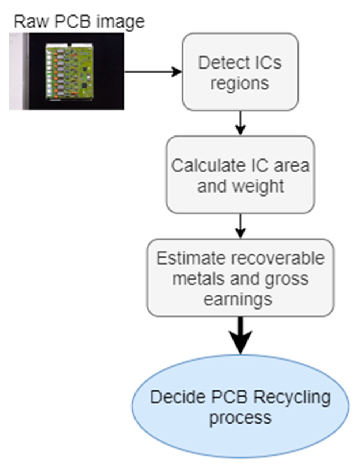
3. Waste Printed Circuit Boards Economic Feasibility Assessment (WPCB-EFA)

Figure 1 shows the outline of the proposed WPCB economic feasibility assessment (WPCB-EFA). The first step is to detect the ICs and then calculate the IC area and weight. With the IC weight, it is possible to use the proposed IC recycling methods to estimate the recoverable metals and the gross earnings [20,21].

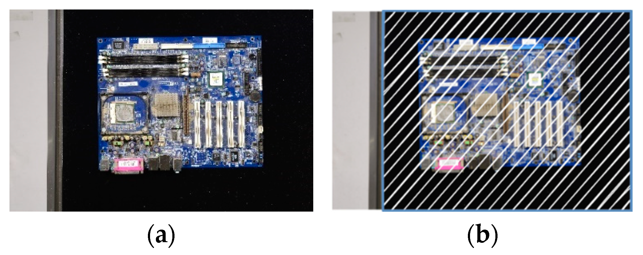
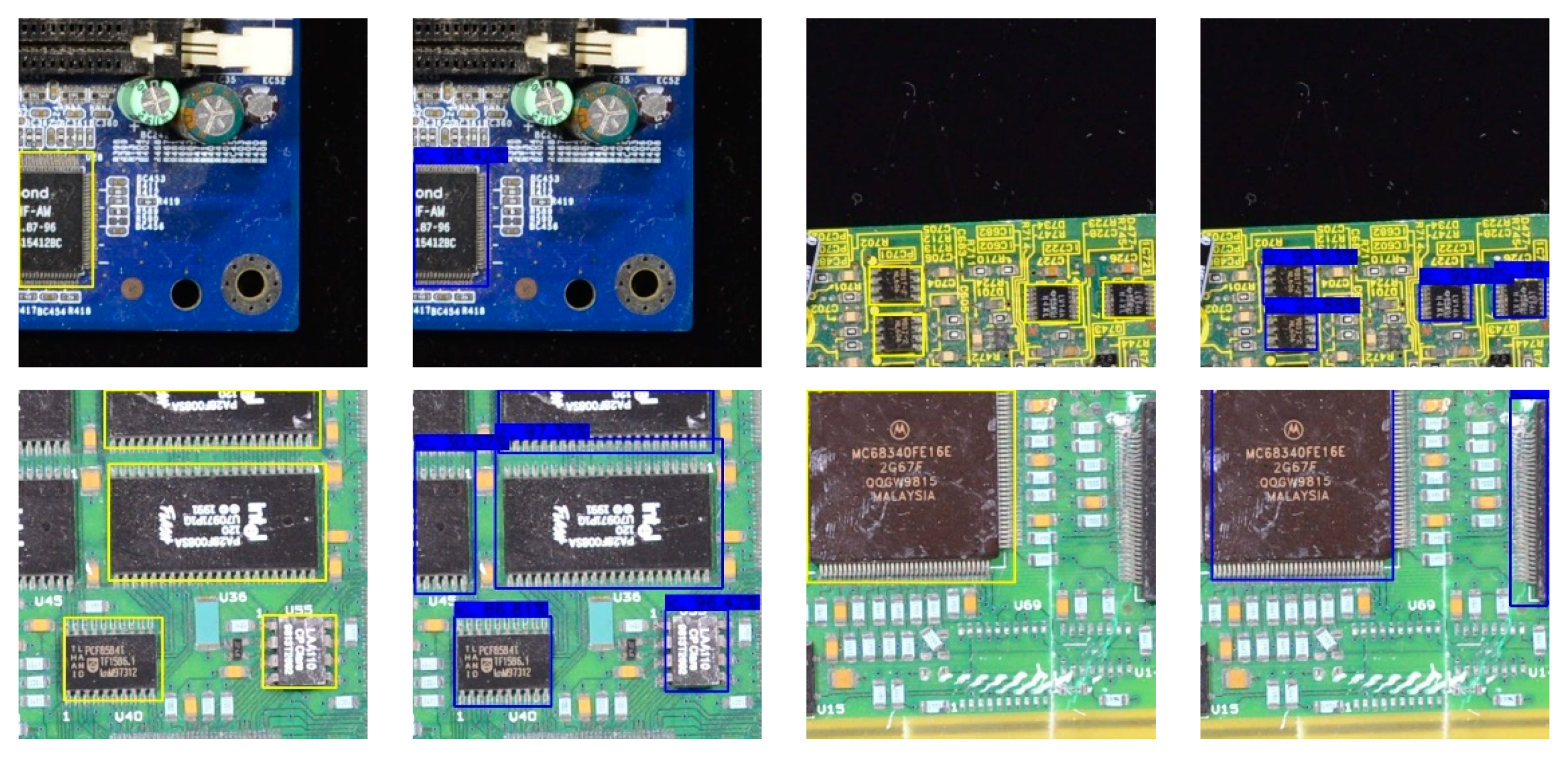
3.1. Detect IC Regions

To detect the ICs in the WPCB images, we evaluated the transfer learning strategy from the pre-trained YOLOv3 model. In order to deal with the few-shot learning problems, one approach is to use prior knowledge and perform a data augmentation procedure [14]. Therefore, we conducted data augmentation in the PCB DSLR dataset to generate smaller sub-images. A sliding window of 416 × 416 pixels generated sub-images by passing through the original image. The training process used only sub-images containing at least a fraction of some IC. After data augmentation, the new dataset had 5347 RGB images containing ICs, each one with a size of 416 × 416 pixels.
Since the IC detector works with chunks of full-resolution WPCB images, the reverse process is necessary to obtain the entire WPCB image’s IC bounding boxes. Given that the WPCB will be in a conveyor belt, we defined the region of interest as the conveyor belt area. Figure 2 illustrates this region of interest. In summary, we removed the region outside the conveyor belt. Since all of the PCB DSLR images were from the same perspective, the region of interest’s coordinates were defined to remove the region outside the conveyor belt.
Therefore, we applied a sliding window approach in the region of interest, similarly to the process of building the training set. The YOLO model processes every image chunk gathered by the sliding window. Then, the YOLO prediction for each image chunk is combined over the original size image to obtain the bounding boxes over the entire WPCB image. Figure 3 shows the prediction result for a full-size image from the PCB DSLR Dataset.
The sliding window stride allows multiple bounding boxes for the same IC. As we were concerned with the IC area, standard non-maximum suppression (NMS) algorithms did not apply to this problem. Therefore, all the predicted bounding boxes with a score higher than the threshold (0.8) were used to produce an image mask. Figure 3 shows the IC image masks for the YOLO predictions and ground truth bounding boxes. Based on the IC image mask, the IC pixel area was calculated.

3.2. Calculating IC Weight

With a WPCB image, it is possible to estimate the surface area of each integrated circuit. However, to calculate the IC’s weight mass, we needed to estimate the average surface density. Texas Instruments (TI) has published an Application Report with information on the IC weight and footprint area of fifteen IC packages [23]. Figure 4 shows the calculated surface density for each IC package and the average IC surface density based on the TI application report. Since most of the IC weight can be assigned to the package, we calculated the average surface density for an IC of 2358 mg/mm2.

3.3. Recycling Economic Evaluation

The general economic evaluation of WPCB recycling was proposed by Niu et al. [2]. The total income for metal powder is given by
G = i = 1 N P i × C i × η M ,
where G is the net income per kilogram metal powder; C i is the commodity cost of the i t h metal element; P i is the composition of that particular metal; η denotes the total weight number; and M is the recycling cost. The recycling cost is highly dependent on the specific production line, so it must be explicitly calculated for one industrial plant. A complete discussion regarding the recycling cost is beyond this paper’s scope since it involves analyzing static and dynamic costs.
Therefore, we can use Equation (1) to calculate the gross profit of IC recycling. Since we are conducting economic evaluation based on visual analysis, the IC weight needs to be estimated from the IC area. So, the IC weight is given by
W = A × S × ρ
where   W is the IC weight; A is the IC surface area in pixels; S is the scale factor from pixel to mm 2 ; and ρ is the IC surface density in g / mm 2 With the IC weight, the gross recycling profit can be calculated as
R = i = 1 N P i × W × C i ,
where P i is the composition of i t h metal (obtained from Table 1); W is the total ICs weight; and C i is the metal market value.

4. Experiments and Results

4.1. Experimental Setup

For the development of the IC object detector, we used the PCB DSLR Dataset [10]. Initially, this dataset has 748 RBG images of WPCBs, with a resolution of 4928 × 3280 pixels, from 165 different boards (three to five images per board). Furthermore, the integrated circuits present on the boards are all labeled, totaling 9313 components.
The WPCBs were extracted from a recycling facility, and some WPCBs had broken parts and dust all over them. The WPCBs had different sizes and shapes, as can be seen in Figure 5. This makes the dataset very close to what is encountered in a real-world scenario. For each PCB, the dataset has images in different positions. This is important because usually, WPCBs are placed on conveyor belts with arbitrary orientation, and a computer-vision system has to perform visual inspection despite the PCB orientation.
In order to obtain the IC surface area, we needed to evaluate the dataset image scale. The silkscreen printing easily identified some IC part numbers on the package. With the measurement of the IC dimensions present in the datasheet, it is possible to calculate the real object size scale. It is important to note that the dataset authors do not provide information about the camera calibration. Table 2 shows the pixel area estimate for a particular IC (part number RTL810L).
For all experiments, we used the pre-trained YOLOv3 provided by Darknet [16]. The fine-tune strategy was to restore the weights from all layers except the last three convolutional layers. Additionally, the YOLOv3 head was fine-tuned with a momentum optimizer and piecewise learning rate starting at 1 × 10⁻⁶, decaying at every five epochs (decay factor of 0.96) until it reached 1 × 10⁻⁶.
With the augmented images dataset, 30 original WPCB images were reserved for the test dataset, and the other images were split into training (80%) and validation (20%). The metric used to evaluate the IC detection was the all-point mean average precision (mAP) [24]. Since there was a single class, the mAP was the same as the AP (average precision) for the IC class, defined as
A P = n ( R n + 1 R n ) P i n t e r p ( R n + 1 )   ,
where R is a recall level and
P i n t e r p ( R n + 1 ) = max R ˜ : R ˜ R P ( R ˜ ) .

4.2. IC Object Detecion

The achieved results for IC object detection are shown in Table 3. The precision was 0.917, and the mAP was 86.77%. Figure 6 shows a qualitative analysis of the results. It is possible to notice small deviations related to bounding boxes, in general, size, centralization, and rotation. However, even with these problems, a proper generalization of the trained model was noticed. For example, in some labels, specific components were not considered integrated circuits, but the model was able to detect them.

4.3. IC Area Results

Using the pixel area scale, Figure 7 shows the predicted and ground truth IC area in mm2 for each WPCB image. It is possible to note that the PCB DSLR Dataset had some images with high IC density (high IC area) and others with very low IC density (low IC area) or even WPCBs without any IC (IC area equaled zero).
Figure 8a shows the graph of the root mean squared error (RMSE) between the ground truth IC area and the YOLO predicted IC area. The highest RMSE value was 6192.38. The RMSE value had a high dispersion (average of 477.12 mm2 and a standard deviation of 698.61 mm2). However, most WPCBs had a percentage error below 2%, as seen in Figure 8b.

4.4. Estimated IC Weight

Using the calculated IC surface density, the total IC weight was calculated based on the total IC area. Table 4 shows the total area and weight for the ground truth and YOLO predictions. The error between the IC weighed calculated from the ground truth, and the one calculated from YOLO predictions was 160.72 g.

4.5. Calculated Recycling Metal Weight

Metals are commodities whose values fluctuate according to market factors. In order to calculate the financial return of each PCB, the average value of metal ore was collected from the stock market. Table 5 shows the estimated return of recycling of all the PCB’s ICs, and the right axis of Figure 7 shows the return of IC recycling for each PCB. The maximum return was USD0.59 (USD0.69 with the IC detector model estimative), and the average return was USD0.05 (standard deviation of USD0.06). It is important to state that these incomes do not consider precious metals as gold and silver, so it is a fraction of the recycling outcomes.

5. Discussion

The proposed economic evaluation output was a total of USD7.44 (USD8.55 with IC detector model) with USD0.59 as the highest value for a PCB and (USD0.69 with IC detector model estimative), and the average return was USD0.05 (standard deviation of USD0.06). However, precious metals (Au, Pd, Pt, and Ag) are a small fraction of the ICs’ mass and were not considered in this small sample. As precious metals are responsible for most of the financial return of WPCB recycling, an increase in the gross income of IC recycling is expected when also recovering precious metals like gold and silver.
The complete estimation of WPCB compositions depends on more data regarding the composition of each electronic component. Research in these directions could reduce the uncertainty in the evaluation of a WPCB composition.
A first application of the proposed method is to cluster PCBs with similar IC densities. Those similar WPCBs could suffer the same recycling process because they probably have similar compositions. Another critical component is the market value of the metal. The market value is positively affected by the purity of the metal. Therefore, depending on the used recycling technique, the gross outcome may be different.

6. Conclusions

Recycling waste printed circuit boards (WPCBs) is very important for recovering high-value metals and providing an environmentally safe destination for these electronic residues. Integrated circuit detection and other components can improve the PCB recycling process since it improves automatic disassembly systems and reuses some components. In this sense, the PCB DSLR public dataset was published to support the research and development of computer-vision strategies for PCB recycling. This paper proposed a WPCB economic feasibility assessment (WPCB-EFA) method for recycling ICs from PCBs. As WPCBs have a high composition diversity, the main goal is to provide information regarding the WPCB composition to guide the recycling process such as the need to dismantle a particular PCB before the physical or mechanical recycling process.
The first step of the WPCB-EFA is to detect ICs in a PCB. Deep learning object detection techniques require large-scale and fully-annotated datasets. Since the PCB DSLR dataset contains only 748 images from 165 different PCBs, transfer learning from the YOLOv3 pre-trained model was evaluated. In order to achieve better results in IC detection, the PCB DSLR Dataset images were split into squares of 416 × 416 pixels, resulting in a total of 5347 images containing integrated circuits. With this image size, YOLOv3 fine-tuning resulted in 0.965 mAP. Qualitative analysis suggests that the model’s errors occur when part of the IC is in the image.
Considering the need for calculating the IC weight, we provide an IC surface density estimate based on the IC manufacturing data. Together with ICs recycling outcomes reported in the literature, we calculated the expected recovery mass for some elements. We noted that some PCBs have much more value than others and may go through different recycling processes. For instance, some PCBs may go to crushing, while others need dismantling before directly crushing. The proposed method may help to optimize the recycling process by such analysis.
The economic evaluation of PCB recycling can be one motivational factor for recycling, aside from the urgent need to deal with electronic waste. In future works, it is necessary to expand the recycling economic evaluation to other PCB components aside from integrated circuits.

Author Contributions

Conceptualization, L.H.d.S.S.; Methodology, L.H.d.S.S. and B.J.T.F.; Software, A.A.F.J. and L.H.d.S.S.; Investigation, L.H.d.S.S.; Resources, S.C.O. and B.J.T.F.; Writing—original draft preparation, L.H.d.S.S. and G.O.A.A.; Writing—review and editing, L.H.d.S.S., G.O.A.A., and B.J.T.F.; Supervision, B.J.T.F. and S.C.O. All authors have read and agreed to the published version of the manuscript.

Funding

This study was financed in part by the Coordenação de Aperfeiçoamento de Pessoal de Nível Superior-Brasil (CAPES)-Finance Code 001, and the Brazilian agencies FACEPE and CNPq.

Institutional Review Board Statement

Not applicable.

Informed Consent Statement

Not applicable.

Data Availability Statement

The PCB DSRL dataset is a public dataset available in [10]. Source code of WPCB-EFA is available in https://github.com/ldhonorato/WPCB-EFA (accessed on 1 January 2021).

Conflicts of Interest

The authors declare no conflict of interest.

References

  1. Marques, A.C.; Marrero, J.-M.; de Fraga Malfatti, C. A review of the recycling of non-metallic fractions of printed circuit boards. Springerplus 2013, 2, 1–11. [Google Scholar] [CrossRef] [PubMed] [Green Version]
  2. Niu, Q.; Xiang, N.; Liu, X.; Duan, G.; Shi, C. The recycle model of printed circuit board and its economy evaluation. In Proceedings of the 2007 IEEE International Symposium on Electronics and the Environment, Orlando, FL, USA, 7–10 May 2007; pp. 106–111. [Google Scholar]
  3. Regel-Rosocka, M. Electronic wastes. Phys. Sci. Rev. 2018, 3, 1–30. [Google Scholar]
  4. Dieste, M.; Viagi, A.F.; Panizzolo, R.; Dos Santos, R.F.; Marins, F.A.S. Reverse logistics models for the collection of Waste Electrical and Electronic Equipment: The Brazilian case. In Proceedings of the 2018 International Conference on Production and Operations Management Society (POMS), Peradeniya, Sri Lanka, 14–16 December 2018; pp. 1–8. [Google Scholar]
  5. Sohaili, J.; Muniyandi, S.K.; Mohamad, S.S. A Review on Printed Circuit Boards Waste Recycling Technologies and Reuse of Recovered Nonmetallic Materials. Int. J. Sci. Eng. Res. 2012, 3, 1–7. [Google Scholar]
  6. Marra, A.; Cesaro, A.; Belgiorno, V. The recovery of metals from WEEE: State of the art and future perspectives. Glob. NEST J. 2018, 20, 679–694. [Google Scholar]
  7. Gao, Z.; Li, J.; Zhang, H.C. Printed circuit board recycling: A state-of-art survey. IEEE Trans. Electron. Packag. Manuf. 2003, 27, 33–42. [Google Scholar]
  8. Lee, C.H.; Chang, C.T.; Fan, K.S.; Chang, T.C. An overview of recycling and treatment of scrap computers. J. Hazard. Mater. 2004, 114, 93–100. [Google Scholar] [CrossRef] [PubMed]
  9. Awasthi, A.K.; Zlamparet, G.I.; Zeng, X.; Li, J. Evaluating waste printed circuit boards recycling: Opportunities and challenges, a mini review. Waste Manag. Res. 2017, 35, 346–356. [Google Scholar] [CrossRef] [PubMed]
  10. Pramerdorfer, C.; Kampel, M. A dataset for computer-vision-based PCB analysis. In Proceedings of the 2015 14th IAPR International Conference on Machine Vision Applications (MVA), Tokyo, Japan, 18–22 May 2015; pp. 378–381. [Google Scholar]
  11. Knoth, R.; Hoffmann, M.; Kopacek, B.; Kopacek, P. Intelligent disassembly of electr(on)ic equipment. In Proceedings of the 2nd International Symposium on Environmentally Conscious Design and Inverse Manufacturing, Tokyo, Japan, 11–15 December 2001; pp. 557–561. [Google Scholar]
  12. Kuo, C.-W.; Ashmore, J.D.; Huggins, D.; Kira, Z. Data-Efficient Graph Embedding Learning for PCB Component Detection. In Proceedings of the 2019 IEEE Winter Conference on Applications of Computer Vision (WACV), Waikoloa Village, HI, USA, 7–11 January 2019; pp. 551–560. [Google Scholar]
  13. Chen, H.; Wang, Y.; Wang, G.; Bai, X.; Qiao, Y. Progressive Object Transfer Detection. IEEE Trans. Image Process. 2020, 29, 986–1000. [Google Scholar] [CrossRef] [PubMed]
  14. Wang, Y.; Yao, Q.; Kwok, J.T.; Ni, L.M. Generalizing from a Few Examples. ACM Comput. Surv. 2020, 53, 1–34. [Google Scholar] [CrossRef]
  15. Kaya, M. Electronic Waste and Printed Circuit Board Recycling Technologies; Springer: Cham, Switzerland, 2019. [Google Scholar]
  16. Redmon, J.; Farhadi, A. YOLOv3: An Incremental Improvement. arXiv 2018, arXiv:1804.02767. [Google Scholar]
  17. Wong, M.H.; Wu, S.; Deng, W.; Yu, X.; Luo, Q.; Leung, A.; Wong, C.; Luksemburg, W.; Wong, A. Export of toxic chemicals—A review of the case of uncontrolled electronic-waste recycling. Environ. Pollut. 2007, 149, 131–140. [Google Scholar] [CrossRef] [PubMed] [Green Version]
  18. Duan, H.; Hou, K.; Li, J.; Zhu, X. Examining the technology acceptance for dismantling of waste printed circuit boards in light of recycling and environmental concerns. J. Environ. Manag. 2011, 92, 392–399. [Google Scholar] [CrossRef] [PubMed]
  19. Huisman, J. QWERTY and Eco-Efficiency Analysis on Cellular Phone Treatment in Sweden; TU Delft: Delft, The Netherlands, 2004; pp. 1–33. [Google Scholar]
  20. Barnwal, A.; Dhawan, N. Physical Processing of Discarded Integrated Circuits for Recovery of Metallic Values. JOM 2020, 72, 2730–2738. [Google Scholar] [CrossRef]
  21. Lee, C.-H.; Tang, L.-W.; Popuri, S.R. A study on the recycling of scrap integrated circuits by leaching. Waste Manag. Res. 2010, 29, 677–685. [Google Scholar] [CrossRef] [PubMed]
  22. Pathak, A.R.; Pandey, M.; Rautaray, S. Application of Deep Learning for Object Detection. Procedia Comput. Sci. 2018, 132, 1706–1717. [Google Scholar] [CrossRef]
  23. Mortan, F.; Wright, L. Quad Flatpack No-Lead Logic Packages; Application Report February 2004; Texas Instruments: Dallas, TX, USA, 2004; pp. 1–47. [Google Scholar]
  24. Padilla, R.; Netto, S.L.; Da Silva, E.A.B. A Survey on Performance Metrics for Object-Detection Algorithms. In Proceedings of the 2020 International Conference on Systems, Signals and Image Processing (IWSSIP), Niterói, Brazil, 3–5 June 2020; pp. 237–242. [Google Scholar]
Figure 1. Diagram of the proposed method evaluation.
Applsci 11 02808 g001
Figure 2. An image sample from the Printed circuit boards digital single-lens reflex (PCB DSLR) Dataset (a) and the region of interest hatchured (b).
Applsci 11 02808 g002
Figure 3. Example of IC (integrated circuit) detection for an entire image: (a) YOLO (object detection model) raw IC detection for the entire WPCB (waste printed circuit board)—a blue bounding box is drawn on each detected IC; (b) Predicted IC mask area—all the bounding boxes are filed and combined over a black background; (c) Ground truth IC area—the mask built on the ground truth bounding boxes.
Applsci 11 02808 g003
Figure 4. Calculated IC surface density for each package and average.
Applsci 11 02808 g004
Figure 5. Some instances of the PCB DSLR Dataset.
Applsci 11 02808 g005
Figure 6. Some partitioned instances of the PCB DSLR Dataset, the left image pair contains the expected results and the right one the obtained results.
Applsci 11 02808 g006
Figure 7. Comparison of IC area (mm2) calculated and real for each PCB.
Applsci 11 02808 g007
Figure 8. Root mean squared error (RMSE) for every WPCB in the dataset (a) and IC area percentual error for every WPCB in the dataset (b).
Applsci 11 02808 g008
Table 1. Physical processing of the discarded integrated circuit (IC) outcomes [20].
Recovered Elements for 1 kg of ICs
Ferrous metal120 gFe68.88 g
Ni31.2 g
Metallic390 gCu311.5 g
Non-metallic490 gSi411.6 g
Table 2. Pixel area estimate.
ImageIC Part NumberDimension in Pixels [px]Datasheet Dimensions [mm]Pixel Area [px/mm2]
Applsci 11 02808 i001RTL810L116 × 11614.00 × 14.0068.653
Table 3. Precision, Recall, and mAP for the IC detector model.
ModelRecallPrecisionmAP
Fine-tuned YOLOv30.8940.91786.77%
Table 4. WPCB’s total IC area and weight.
MetricPredictedGround TruthError
Total IC Area (mm)525,828.2457,667.3714.89%
Total IC Weight (g)1239.91079.1814.89%
Average RMSE (mm)477.12 (698.61)
Table 5. Total IC recycling estimation outcomes.
MetalMetal Value
(USD/Ton)
Recycling Rate
(g of Metal/Kg of IC)
IC Detection ModelGround Truth
g of MetalUSD Returng of MetalUSD Return
Fe10068.8885.400.0085474.330.00743
Ni13,88731.238.680.5372233.670.46758
Cu6440331.5411.032.64701357.742.30390
Si10,500411.6510.345.35860444.194.66400
Total--1045.468.55909.947.44
Publisher’s Note: MDPI stays neutral with regard to jurisdictional claims in published maps and institutional affiliations.

