Article

Fast and Low-Cost Synthesis of MoS2 Nanostructures on Paper Substrates for Near-Infrared Photodetectors

1
Laboratório de Óptica e Optoeletrônica, Departamento de Física, Universidade Estadual de Londrina (UEL), CP6001, Londrina, Paraná CEP 86051-970, Brazil
2
CENIMAT|i3N, Departamento de Ciência dos Materiais, Faculdade de Ciências e Tecnologia, Universidade Nova de Lisboa (UNINOVA), 1099-085 Lisboa, Portugal
3
Laboratório de Fotônica e Materiais Nanoestruturados, Departamento de Física, Universidade Tecnológica Federal do Paraná (UTFPR), Londrina, Paraná CEP 86036-370, Brazil
*
Authors to whom correspondence should be addressed.
Appl. Sci. 2021, 11(3), 1234; https://doi.org/10.3390/app11031234
Submission received: 30 December 2020 / Revised: 19 January 2021 / Accepted: 25 January 2021 / Published: 29 January 2021

Abstract

:

Featured Application

This work presents an analysis of time and temperature influence of microwave-assisted hydrothermal synthesis on the direct growth of 2D-MoS2 nanostructures on cellulose paper substrates, and the production of MoS2-based low-cost photosensors with high responsivity and detectivity values.

Abstract

Recent advances in the production and development of two-dimensional transition metal dichalcogenides (2D TMDs) allow applications of these materials, with a structure similar to that of graphene, in a series of devices as promising technologies for optoelectronic applications. In this work, molybdenum disulfide (MoS2) nanostructures were grown directly on paper substrates through a microwave-assisted hydrothermal synthesis. The synthesized samples were subjected to morphological, structural, and optical analysis, using techniques such as scanning electron microscopy (SEM), X-ray diffraction (XRD), and Raman. The variation of synthesis parameters, as temperature and synthesis time, allowed the manipulation of these nanostructures during the growth process, with alteration of the metallic (1T) and semiconductor (2H) phases. By using this synthesis method, two-dimensional MoS2 nanostructures were directly grown on paper substrates. The MoS2 nanostructures were used as the active layer, to produce low-cost near-infrared photodetectors. The set of results indicates that the interdigital MoS2 photodetector with the best characteristics (responsivity of 290 mA/W, detectivity of 1.8 × 10⁹ Jones and external quantum efficiency of 37%) was obtained using photoactive MoS2 nanosheets synthesized at 200 °C for 120 min.

Graphical Abstract

1. Introduction

Since its discovery in 2004, graphene has become one of the nanomaterials of great interest in the construction of devices, due to its high electronic conductivity, mechanical flexibility, and low production cost [1]. Despite the good results obtained with graphene [2,3], the absence of energy bandgap restricts its application in some devices, such as photodetectors, mostly due to low intrinsic responsivity. This led to the development of a series of other two-dimensional materials with different characteristics, such as the hexagonal boron nitride [4], silicene [5], borophene [6], black phosphourous [7], and two-dimensional transition metal dichalcogenides (2D TMDs) [8]. The latter have been thoroughly explored in recent years for several applications [8].
Among the 2D TMDs materials, composed of a transition metal (M) and a chalcogen (X) with generalized form MX2 in which M = Mo, W, Nb, Ta, Hf, Pt, and so on, and X = S, Se, Te, the MoS2 nanostructures has generated great interest in the scientific community [8,9,10]. Featuring a metastable metallic phase (1T), which can be stabilized or converted to a stable semiconductor phase (2H) by the appropriate heat treatment [11] or use of microwave radiation [12], MoS2 has unique characteristics, such as high carrier mobility, strong electron-hole confinement and variable bandgap (1.20 to 1.89 eV) [13,14]. The bandgap of the MoS2 increases with the decrease of the crystal thickness, to below 100 nm, due to the quantum confinement effect [15], and reaches 1.89 eV for a single monolayer [13]. Thus, it can cover an extent NIR (near-infrared) electromagnetic spectrum (6560 to 10,332 nm) by changing the monolayer number. Additionally, the material changes its electronic structure from an indirect bandgap, in its bulk form, to a direct bandgap in the MoS2 monolayer [16], enabling optical applications. The relationship between its optical and electrical characteristics with the number of stacked layers and the control of the 1T and 2H phases turns the MoS2 into a material of great interest for applications in chemical sensors [17], hydrogen evolution reaction [18], electronic devices [19], sodium-ion battery [20], and photodetectors [21,22].
The most commonly used synthesis methods of the two-dimensional MoS2 are exfoliation (liquid [23,24] and mechanical [24]), chemical vapor deposition (CVD) [25], and hydrothermal [26]. Due to a better relationship between uniformity, the quantity of produced material and production cost, the hydrothermal method has been the most applied in the synthesis of MoS2 nanostructures, usually presenting synthesis times between 20 and 24 h [27,28]. The microwave-assisted hydrothermal method has proved to be a good alternative to the conventional hydrothermal method, offering shorter synthesis times due to “molecular heating”, consequently lower energy consumption, enhanced reaction selectivity, and homogeneous volumetric heating [29,30,31]. This method also allows the direct growth of the material on a substrate, being an alternative to conventional deposition or costly transfer methods [28,32]. Synthesis parameters, such as time and temperature, as well as the chemical processes involved in the production of the material, allow the direct growth of the MoS2 nanostructures on flexible substrates [28], like cellulose-based substrates [33,34,35]. These advantages will have impact in the development of paper-based electronics that emerge as a future alternative to traditional electronics, seeking low-cost electronic systems and components which can be environmentally friendly [36,37,38]. To meet the requirements imposed on this new generation of devices, different methods of producing materials and printing technologies are employed for the production of electronic devices [36,38,39,40], like solar cells [41], thin film transistors [42], light emitting devices [43], electrochromic devices [44], and photosensors [28], among others.
In this work the authors adopted the microwave-assisted hydrothermal method, with different synthesis parameters, for direct growth of MoS2 nanostructures on tracing paper substrates. Structural and morphological characterizations of the MoS2 nanosheets were performed, where it was possible to observe the dispersion of the 2H and 1T phases of the nanostructures grown on paper, making these samples potentially interesting for applications in optoelectronic devices. Thus, near infrared photodetectors of MoS2 nanostructures, grown on cellulose substrates, were built with different synthesis parameters. These interdigital MoS2 photodetectors (with detection at 980 nm) were obtained with high responsivity (290 mA/W) and detectivity of 1.8 × 10⁹ Jones. These devices presented higher responsivity values than that reported in the literature, as compared with MoS2 photodetectors produced by the conventional hydrothermal method.

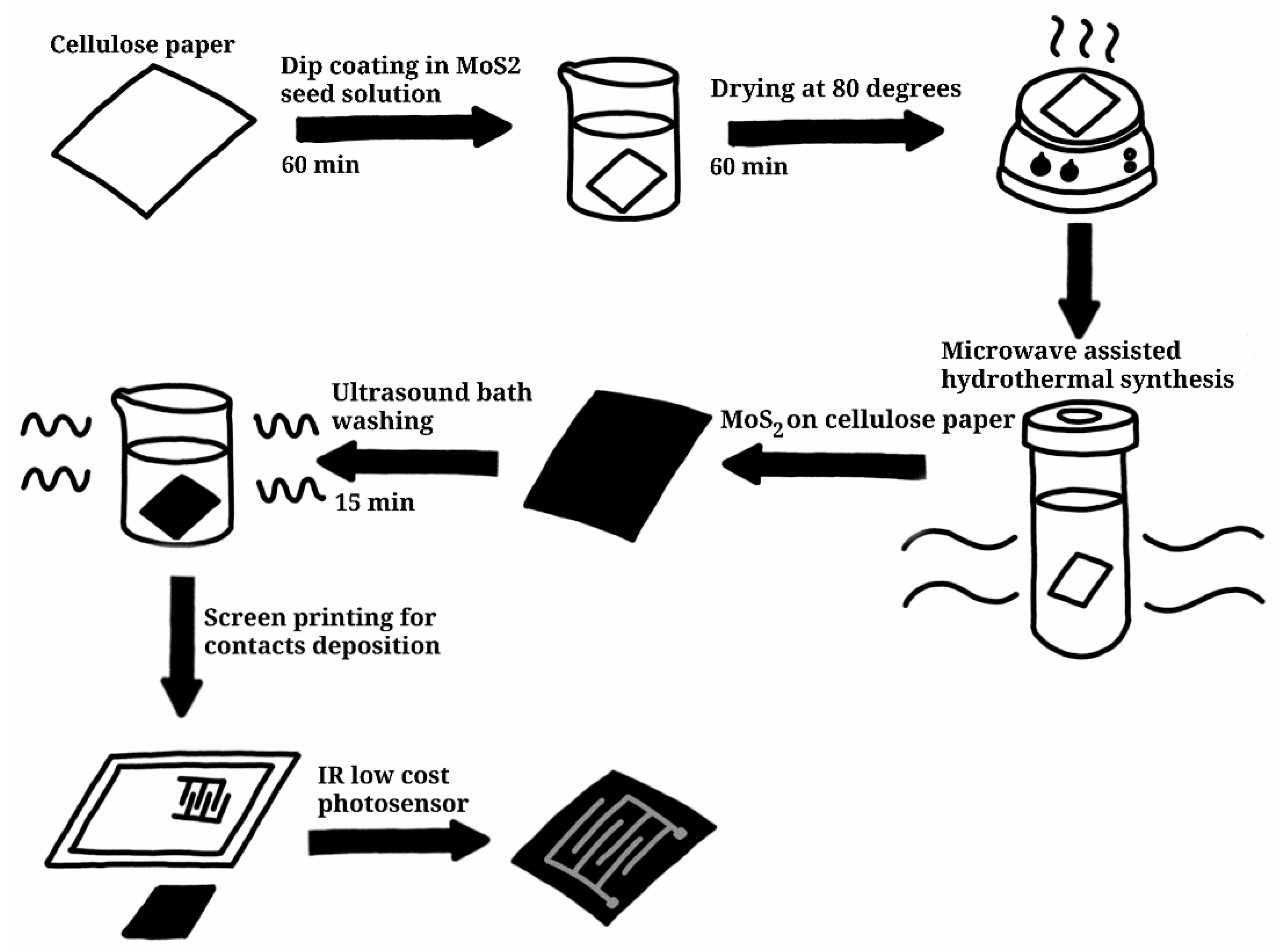
2. Materials and Methods

Molybdenum disulfide (MoS2) nanosheets were grown on cellulose paper substrates by a microwave-assisted hydrothermal method optimizing the hydrothermal temperature and reaction time. Sodium molybdate dihydrate (Na2MoO4.2H2O) and thiourea (CS(NH2)2) were used as precursors of molybdenum and sulfur, respectively. Cellulose paper was used as a substrate, which was previously washed by sonication in deionized water and by acetone and isopropyl alcohol, both for 15 min.
For direct growth on the cellulose fibers, the substrates were previously immersed in a seed solution composed of sodium molybdate and thiourea (1:4) for 60 min. After that time, the substrates were dried on a hotplate at 80 °C for 60 min. Substrates with deposited seeds were placed in a hydrothermal reactor with nutrition solution also composed of sodium molybdate and thiourea (1:4). Then, they were taken to the microwave oven for synthesis that was carried out with a power of 100 W, maximum pressure of 280 psi, and with different values of temperature and time of synthesis. Three different synthesis temperatures were used: 190 °C, 200 °C, and 220 °C. These were chosen to apply the shortest possible time for the growth of the nanostructures, corresponding to each temperature used, until the maximum time of 120 min. Thus, the different temperatures and synthesis times used were: 190 °C for 30, 45 and 120 min, 200 °C for 15, 30, 45, 60 and 120 min, 220 °C for 05, 15, 30, 45, 60, and 120 min. After the growth of the MoS2 on the cellulose fibers, the paper with the grown nanostructures were washed with ethanol in ultrasound for 15 min to remove the nanostructures not fixed on the sample’s surface. Finally, the samples were dried in a nitrogen flow.
Interdigital contacts were deposited by the screen-printing technique using commercial conductive ink CRSN2442 Suntronic, composed of silver nanoparticles dispersed on the solvent (solvent-based), acquired from Coats Screen Inks GmbH. The interdigital electrodes have a total dimension of 10.0 × 6.0 mm, 500 µm electrode wide and a 500 µm active channel between the electrodes.
Structural and optical properties of the MoS2 nanostructures, grown on cellulose paper substrate, were studied by X-ray diffraction (XRD), scanning electron microscopy (SEM), and micro-Raman spectroscopy. The crystal phase was obtained by X-ray diffraction (X’Pert PRO MPD), using Cu-kα radiation (λ = 1.540598 Ǻ). The XRD patterns were collected in symmetric configuration in the 2θ range of 5−70°, using a step angle of 0.05°, step time of 2 s, operating at 40 kV tension and 30 mA current. The morphology was studied by scanning electron microscopy (Carl Zeiss AURIGA CrossBeam workstation). Raman measurements were performed in a Renishaw inVia Reflex micro-Raman spectrometer equipped with an air-cooled CCD detector and a HeNe laser operating at 50 mW of 532 nm laser excitation. The spectral resolution of the spectroscopic system is 0.3 cm−1. The laser beam was focused with a 50 × Leica objective lens (N Plan EPI) with a numerical aperture of 0.75. An integration time of 3 scans of 1.5 s each was used for all single-scan measurements to reduce the random background noise induced by the detector, without significantly increasing the acquisition time. The intensity of the incident laser was 2.5 mW. Triplicates were taken for all spectra. The spectrograph was calibrated between different Raman sessions using the Raman line at 521 cm−1 of an internal Si wafer for reducing possible fluctuations of the Raman system. All spectra were recorded at room temperature. Raw data were collected digitally with the Wire 5.0 software for processing. The characterization of the photodetectors was performed with the use of an AUTOLAB potentiostat (PGSTAT204) for ixV electrical measurements and chronoamperometry and a 980 nm diode laser for irradiation of the sensors, under ambient conditions. The power of the laser light was recorded using a handheld digital power meter console (PM100D) from THORLABS. Neutral density filters were used to vary the excitation power incident on the devices.

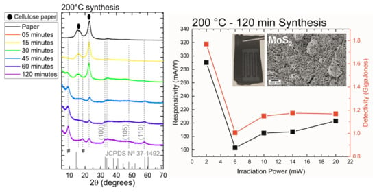
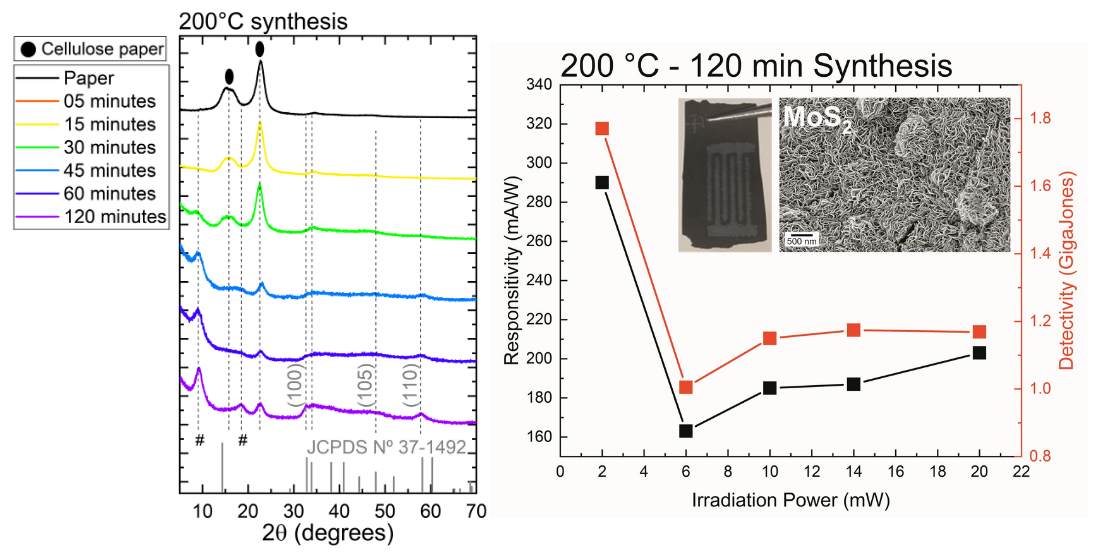
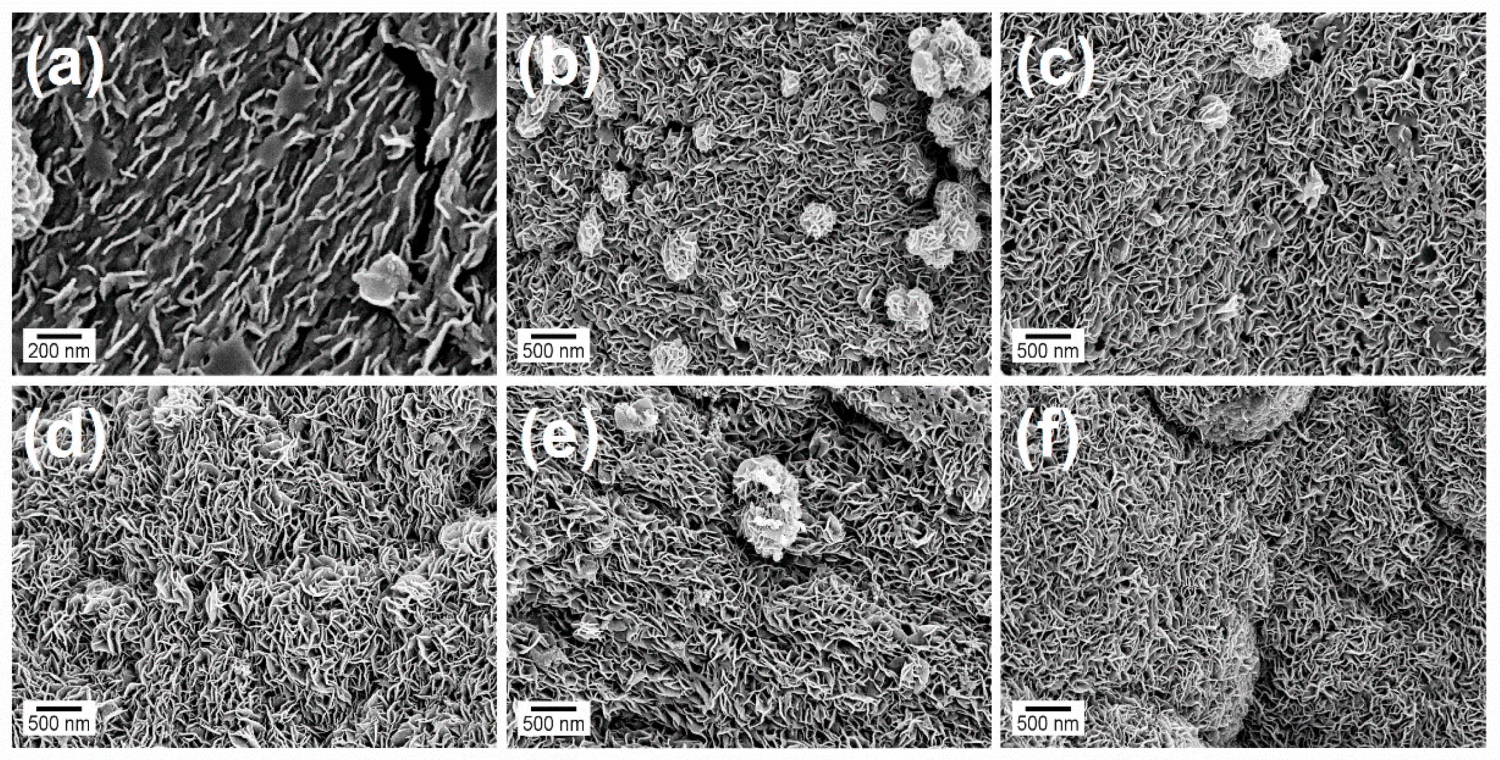
3. Results and Discussion

The microwave-assisted hydrothermal synthesis method was used for the direct growth of MoS2 nanostructures on cellulose paper substrates due to the ease of the technique’s application, as well as its ability to change synthesis parameters to optimize the produced structures [29,30,31]. The growth was carried out using a two-step process, where the synthesis is performed on a substrate with a thin layer of deposited seeds.
For construction of NIR photodetectors, a layer of interdigital silver electrodes was deposited on the layer of the MoS2 nanostructures using the screen-printing technique. Further details on the growth of nanostructures and the construction of the devices can be found in the Experimental Section. Figure 1 shows a diagram of the MoS2 nanostructures synthesis and the photodetector production.
Figure 2 shows SEM images of the samples synthesized with a synthesis temperature of 220 °C at different times.
Microscopy images show that the beginning of the growth process is characterized by the formation of vertically aligned MoS2 nanosheets on the paper surface (see also Figure S1 in the Supplementary File), while the paper fibers are not fully covered. For longer synthesis times, the surface of the paper becomes completely covered by vertically aligned MoS2 nanosheets, regardless the temperature. The effect of temperature is noticed on the time required to observe the first nanosheets on the paper surface. Such a result is expected since, for lower temperatures, the solution is exposed to lower energies during the synthesis process, requiring a longer time for nanomaterial formation. At 190 °C, it is possible to observe that, even for the longest synthesis time (120 min), the profile of the paper fibers is still perceived, indicating that it was not possible to form a thick and uniform nanostructure layer. On the other hand, at 200 °C the fibers are uniformly coated with a thick layer of MoS2 nanosheets. It is important to note that the samples synthesized at this temperature had a more uniform surface profile than the samples produced by the conventional hydrothermal method reported in the literature [28,33,35], which generally have agglomerations of MoS2 nanosheets in microspherical profile. A surface totally covered with nanostructures is also observed in the samples synthesized at 220 °C. However, at this temperature, it is possible to observe that, for longer synthesis times, the sample surface has regions with a spherical profile very similar to those synthesized by the conventional hydrothermal method [28,32]. This indicates that there was the production of a large number of nanostructures during the synthesis process, where they tend to agglomerate in spherical shape, microflowers, formed by nanosheets. The growth kinetics of MoS2 nanostructures on cellulose paper and other flexible substrates was recently discussed by Sahatiya et al. [28] through classical nucleation and growth theory. These spherical structures are formed when there is excessive nanosheets growth, which generally occurs for longer synthesis times or for MoS2 synthesis without the presence of the substrate [26]. In the synthesis with direct growth on substrate, the excess of grown nanostructures ends up detaching from the paper surface and agglomerating into spherical particles to decrease the surface energy. Note the early formation of these small flowers for samples synthesized at 200 °C (Supplementary Figure S1).
Figure 3 shows XRD diffractograms at different temperatures and synthesis times of the MoS2 nanostructures, in addition to the XRD diffractogram of cellulose paper and the JCPDS n° 37-1492 card pattern of 2H-MoS2 for comparison purposes [28,45]. Dashed vertical lines are used to facilitate the identification of phases in the diffractograms obtained at different temperatures and synthesis times. It is possible to identify regions, close do 15° and 22°, with the characteristic peaks of the cellulose diffractograms, the 2H-MoS2 phases with XRD peaks at ~32.8°, ~49.8°, and 57.8° relative to (100), (105), and (110) planes, respectively. For 2θ > 30° the XRD peaks fit well with JCPDS card n° 37-1492, where the presence of (100) and (110) peaks, ate ~32.8° and 57.3° respectively, show that the samples present similar atomic arrangement along the basal planes with the bulk MoS2.
According to the standard 2H-MoS2 diffractogram pattern, represented by the JCPDS card n° 37-1492 shown in Figure 3, there is a diffraction peak at 14.4° regarding the plane (002) of the layered material. However, two other peaks appear in the diffractogram, at 9.3° and 18.6°, identified in Figure 3 by # symbols. MoS2 is a representative 2D layered material and the weak van der Waals interaction between MoS2 layers favors the intercalation of molecules and ions in this space [32,46]. The interlayer distance of the (002) plane, referring to the 14.4° peak, of intercalation-free MoS2 is 0.62 nm, while the corresponding interlayer distances of 9.4° and 18.6° peaks, present in the diffractograms of the synthesizes samples, were 0.93 nm and 0.49 nm, respectively, calculated using the Bragg equation. Several groups attribute the interlayer distances of 0.93 nm and 0.49 nm to the distance between two adjacent MoS2 expand layers—resulting from the intercalation of different materials as CTAB [47], mesoporous carbon (MoS2/m-C) [48], NH4+ [49], and NH3 molecules [46]—and that distance between intercalated molecules and the adjacent MoS2 layers, respectively [32,47,48,50]. Other authors have attributed the 18.6° peak to a second-order diffraction [49] It is important to note that, while some authors have attributed the shifted 9.4° and 18.6° peaks to the presence of 1T-MoS2 phase [49,51], Lei et al. [52] have alerted about the difficult to use the expanded interlayer spacing of MoS2 as direct evidence to confirm the existence of the 1T-MoS2 phase.
Liu et al. have shown that the use of the Na2MoO4.2H2O and CS(NH2)2 with high thiourea concentration induce the formation of ammonium ion intercaled into MoS2 layer [49]. In the synthesis procedure presented in this work, Na2MoO4.2H2O and thiourea were used as precursors of molybdenum and sulfur, respectively, in the proportion of (1:4). Thus, we believe that the MoS2 nanosheets grown on cellulose paper substrates by a microwave-assisted hydrothermal method present NH4+ intercaled between layers of MoS2.
It should also be noted that there is an decrease in the intensity of the cellulose diffraction peaks when subjected to heat treatments (probably associated with crystallinity of the cellulose) [53]; even so, the diffraction peaks of MoS2 stand out in the diffractogram for high synthesis times, due to the greater amount of nanomaterial grown on the paper surface, for (100), (105) and (110) planes, or the possible increase of the intercalation with the synthesis times, for the 9.4° and 18.6° peaks.
It can be noted that there is a continuous increase in peak intensity at 9.2° up to 30 min, in samples synthesized at 220 °C. Then the intensity of the entire diffractogram, including those peaks related to cellulose paper, starts to decrease for higher times. The high temperature leads to degrading the paper structure and can affecting the growth process for longer synthesis times, leading to less production of nanostructures on the substrate surface. This result is in line with what is reported in the literature, which leads to cellulose degradation processes starting above 200 °C [53]. In summary, the growth process of the MoS2 on paper substrate seems to be better at 200 °C.
For a complementary analysis of the presence of 1T and 2H-MoS2 phases, Raman spectroscopy measurements were performed, looking for the presence of characteristic peaks of these phases on the samples. After confirming the presence of both phases in the synthesized samples by Raman spectroscopy, an analysis of the spatial distribution of 1T and 2H-MoS2 was performed by the micro-Raman technique. By mapping an area of 225 μm [2] and using steps of 1 μm, the regions of the spectra between 146 to 148 cm−1 (referring to the main vibrational mode of the 1T phase), and between 378 to 385 cm−1 (referring to the E12g vibrational mode of the 2H phase) [12,46], were highlighted. The Raman spectrum and the micro-Raman mapping of the samples synthesized at 220 °C, for times of 05 and 120 min, are shown in Figure 4.
As can be seen in Figure 4a,b, it was possible to identify characteristic Raman peaks of the 1T (vibrational modes J1, J2 and J3) and 2H (vibrational modes E12g and A1g) phases in the sample spectrum [46], thus confirming the presence of both phases in the synthesized nanostructure. Figure 4c,d shows the micro-Raman mapping, confirming the presence of both phases, the 1T (blue) and the 2H (green), in both samples and in the same space region. These phases are not occupying well-defined regions, but they are dispersed throughout the mapping area. This behavior is observed for all samples (regardless synthesis time and temperature), as shown in Figure 4 and Figure S2 of the supplementary information. The dispersion of the metallic and semiconductor phases of MoS2 in the samples may be associated with the continuous production of the metallic phase during synthesis. Over time, the 1T phase is converted to a 2H phase, due to the low stability of the metallic phase and presence of microwave radiation during the synthesis process [12]. Thus, the 1T and 2H phases are present in the samples, as can be seen in the diffractogram of the sample synthesized at 200 °C for 120 min. The greater dispersion of phases on the surface of the substrate can be good for certain applications, since it increases the metal/semiconductor interface (1T/2H) which leads to greater carrier mobility due to the presence of the 1T phase.
As shown in Figure 1, low-cost interdigital photodetectors were built on cellulose paper substrate with a MoS2 active layer synthesized by the microwave-assisted hydrothermal method at different temperatures and times. Figure 5a–c show the current x voltage curves under laser illumination (980 nm) of the photodetectors with a MoS2 photosensitive layer synthesized at 190, 200, and 220 °C, respectively. The curves are linear and symmetric for the small bias voltage, indicating a ohmic-like contact as observed for the single-layer MoS2 phototransistor synthesized using the CVD technique [54], or by photodetector built with a multilayer MoS2 synthesized by the conventional hydrotermal method, using in this case Ag NPs (nanoparticles) as contact [28]. The small bandgap energy of the multilayer MoS2 may generate a very small Schottky barrier between Ag NPs electrodes and MoS2. After illumination, carriers are injected into the small conduction band of the multilayer MoS2 generating photocurrent. The photocurrent increase can be associated with a bias voltage through to the reduction of the carrier transit time (τtransit = l2/µV), where l is the length of the channel, µ is the carrier mobility, and V the bias potential [22].
The curves in Figure 5b,c, for longer synthesis times, present a strong increase in the current x bias voltage (with a non-linear behavior) for bias voltages higher than ~2V. This non-linearity in the IxV curve is less intense in the samples synthesized at lower temperature, 190 °C—Figure 5a, and in the samples with shorter synthesis times for the synthesis temperatures of 200 and 220 °C, possibly due to the smaller amount of MoS2 material. Figure 5d–f show that there is an increase in both the dark current and the photocurrent, a result that goes according to the discussion held for Figure 5a–c. The increase in the dark current with synthesis time can be associated with the presence of the metallic phase and trap states.
To evaluate the infrared photosensors, figures of merit Responsivity (R) and Specific Detectivity (D*) were used, which can be calculated using the equations R = (Ion-I0ff)/P and D* = R/√((2eI0ff)⁄A). Here, Ion is the generated photocurrent in the device under illumination, Ioff is the dark current, P is the incident light power on the effective area of the device, e is the elementary charge and A is the effective surface area. Figure 6 shows that R and D* values increase with increasing of the synthesis time for three synthesis temperatures and for a bias voltage of 4V. The device built with a sample synthesized at 200 °C for 120 min has the highest value for both D* and R. There is also a big increase of these values for synthesis time longer than 60 min (see yellow curve). The decrease in the R value obtained in the sample synthesized at 220 °C for 120 min, when compared to the sample synthesized at 200 °C for 120 min, may be attributed to the degradation of the cellulose paper.
Therefore, the experimental data show that the temperature of 200 °C and time of 120 min were the best conditions for the production of near infrared photodetectors based on MoS2 active layer grown directly on cellulose paper substrates by the microwave-assisted hydrothermal method. This R value is above the value reported in the literature for photodetectors with active MoS2 layer produced by the hydrothermal method with the same structure. Nahid Chaudhary et al. [55] for example, obtained the maximum R value of 23.8 µA/W for excitation at 635 nm, and Parikshit Sahatiya et al. [28] obtained the R value of 60 µA/W for excitation at 554 nm.
It is important to note that temperatures above 200 °C have generally been used in the literature for synthesis of MoS2, or heat treatments have been made after the synthesis to increase the fraction of phase 2H over phase 1T. At 200 °C (as in this work), we still have a large proportion of the 1T phase when compared with samples synthesized by the conventional method followed by heat treatment [13,28]. Therefore, we believe that the increase in the 1T/2H interface, caused by the simultaneous and continuous formation of the metallic phase and its conversion to the semiconductor phase, and the consequent increase in the mobility of carriers in the sample, is of great importance to obtain high values of responsivity in MoS2 photodetectors. The interface between the paper substrate and the MoS2 layer may be another important characteristic for devices, once it can be a source of trap states [54] and temperature and time synthesis had a greater effect on the photoconductivity. Thus, the quick increase of the photocurrent to bias voltage (>2 V), as observed in Figure 5, can be associated with the detrapping charge from trap states. It is known that photogain in photoconductors increases as carrier lifetime and decreases as transit time G = τlifetransit [22].
Figure 6 shows the external quantum efficiency (EQE) of the devices. EQE was obtained by using EQE(%) = Rhc/(λe)x100. Here, R is the responsivity, h is the Planck’s constant, c is the speed of light in vacuum, e is the elementary charge, and λ is the wavelength of the excitation light. As can be seen, the EQE increases as the time synthesis increases, similar to R and D*. The device built from MoS2, synthesized at 200 °C for 120 min, presents an EQE value of 26%.
The MoS2 photodetector has a relatively high R value, compared to other similar devices based on MoS2 synthesized by the hydrothermal method. The rise and the decay response time has high values (τrise = 3.7 s e τdecay = 4.7 s) which may be associated with the high concentration of the metallic phase in MoS2 and trap states in the MoS2 and/or paper/MoS2 interface. In comparison, the HfO2-gated single-layer MoS2 phototransistors, with high responsivity due to the photogate effect, present a slow response of 0.6–9.0 s. In this case, the slow response time and the high responsivity was induced by the trap states in the MoS2 or MoS2/SiO2 interface [54] Jin et al. [56] deposited Ag NPs on monolayer MoS2 phototransistor and obtained a very high R value and slow response time of 18.7 s, showing other strategy to induce photoconductive effect. The improvement was attributed to the localized surface plasmon resonance of Ag NPs with the increase of light absorption and carrier injection from Ag NPs to MoS2 under illumination. Thus, we believe that, in our device, the surface plasmon resonance in the Ag NPs electrode is light excited and generates hot electrons via nonradiative decay plasmonic resonance, since the Ag NPs show a plasmonic resonance signal in the near-infrared region, as shown in Figure S3 in the supplementary file. The energy of the hot electrons may be greater than the small Schottky barrier between Ag NPs and MoS2, and it can be injected into the MoS2 multilayer generating a photocurrent [57,58,59]. Additionally, the effect of the MoS2 phases (1T and 2H) on the electrical performances of hybrid PDs was compared by Wang et al. [60] and results indicated that the metallic 1T phase exhibited a high R value. However, these devices showed low on/off ratios (<2) and slow response times (0.75 s) due to their metallic conducting nature similar to that of the graphene. On the other hand, the semiconducting 2H phase demonstrated lower R value and fast response time (<25 ms). Thus, we believe that our PDs built with MoS2 synthesized at 200 °C for 120 min presented higher metallic phases than other devices built with materials synthesized for other temperatures and times, and that the hot electrons from Ag NPs could be contributing to the photocurrent improvement. Therefore, the contact between Ag NPs and the MoS2 multilayer must convert from a small Schottky junction to an Ohmic-like contact when the device is illuminated, as observed in Au nanorods/Perovskite photoconductor [56,61]. The device works as a light illuminated photoconductor, explaining the slow response time and high R compared to a similar device based on a MoS2 synthesized by the conventional hydrothermal method [28,55].
Figure 7 shows the dependence of the photocurrent (Ion-Ioff) as a function of the light power on the photosensor synthesized at 200 °C for 120 min.
Figure 7a shows a decrease in photocurrent behavior with decreasing light power intensity. This is an expected result, since with the decrease in the incident light power, there is a decrease in the number of photons reaching the sensor and, consequently, there is a decrease in the number of carriers promoted from the valence band to the conducting band of the MoS2 nanostructures. With the decrease in the number of carriers in the conduction band, there is a decrease in the generated photocurrent (Ion-Ioff). An analysis of the relationship between the generated photocurrent and the incident light power on the photodetector is showed in the inset of Figure 7a, where a fitting with power law is used ( I = A P θ ). Here A is a proportionality constant and θ is the exponent that determines the relationship between the photogenerated current and the light source power. From the adjustment, a linear relationship is observed ( θ = 1.1 ± 0.1 ). Similar behavior of the photocurrent with light intensity was observed for the single-layer MoS2 phototransitor [54]. Figure 7b shows the relationship between responsivity/detectivity and the light source power used. Note that the highest responsivity and detectivity values (290 mA/W and 1.8 × 10⁹ Jones) occur for the power of 2 mW. In the range of 6 to 2 mW, the responsivity and detectivity values increase rapidly with decreasing power (these results indicate that for lower radiation intensity, in the µW range, the photodetector can present very high responsivity values—these results are not showed here). This behavior has been associated with the increase in the recombination probability as carriers photoexcitation increases [59]. EQE measurements (inset of Figure 7b) obtained at various excitation powers show that the EQE gradually increases as the power decreases, similar to the results for the graphene–MoS2–graphene devices (responsivity of ≈ 0.2 A W−1 and EQE = 55%) [62].

4. Conclusions

MoS2 nanostructures were grown directly on cellulose paper substrates using the microwave-assisted hydrothermal synthesis method with different temperatures and synthesis times. Variations were observed in the amount of MoS2 grown on top of cellulose fibers as a function of the synthesis parameters. The analysis also showed the distribution of the metallic and semiconductor phases of the MoS2 nanostructures throughout the sample, generating metal/semiconductor interfaces. Near-infrared sensors were produced from the synthesized samples, where the screen-printing technique was used to deposit interdigital Ag NPs contacts in the samples. The results of the electrical characterizations showed an improvement in the performance of the sensor with the increase in nanostructures synthesis time, for the three temperatures of synthesis used. Such results can be explained by the increase in the amount of MoS2, according to the model created for the sensors operation. Based on the data analysis, the photodetector produced from the sample synthesized at 200 °C and 120 min presented a high responsivity value (290 mA/W), a specific detectivity value (1.8 × 10⁹ Jones) and an external quantum efficiency of 37%, with response times τrise = 3.7 s and τdecay = 4.7 s. The sensors produced from the samples synthesized at a temperature of 220 °C also showed high values of responsivity, however, the high temperature causes substrate degradation, making the device fragile and the application difficult. The improvement in the responsivity value of the photodetector can be associated with the photoconductive effect due to three probably factors: (i) the high concentration of the metallic 1T phase in MoS2 layers; (ii) trap states in the MoS2 and/or paper/MoS2 interface; and (iii) hot electron injection from surface plasmon resonance in the Ag NPs electrodes to MoS2 nanomaterial.
An analysis of the photocurrent dependence as a function of the incident radiation power on the sensor showed a linear dependence of the device’s photocurrent in relation to the power of the light source. The responsivity showed a great increase with the reduction of the irradiation power, at the value of 290 mA/W for the power of 2 mW. This result must be associated with the increase in the probability of recombination with the increase in the photoexcited carriers. This work provides a functional example, as well as a promising strategy, to improve the performance of 1T/2H MoS2-based photodetectors. Further studies on the surface state passivation for device optimization, for example, will be conducted to improve photocurrent in MoS2 photodetector synthesized by the microwave-assisted hydrothermal synthesis method.

Supplementary Materials

The following are available online at https://www.mdpi.com/2076-3417/11/3/1234/s1, Figure S1: SEM images of the MoS2 nanostructures grown directly on cellulose paper substrates with different temperature and time of synthesis, Figure S2: Micro-Raman mapping and detachment of phases 1T (blue) and 2H (green) in samples of MoS2 nanostructures grown directly on paper substrates with different temperature and time of synthesis, Figure S3: Absorbance spectrum of silver nanoparticles ink in an isopropyl alcohol solution.

Author Contributions

Conceptualization, N.J.A.C., C.G., P.B., L.P., E.F., R.M., E.L. and S.A.L.; Data curation, N.J.A.C., C.G., M.J.d.O., D.N., P.B., L.P., E.L. and S.A.L.; Formal analysis, N.J.A.C., C.G., M.J.d.O., D.N., P.B., L.P., E.L. and S.A.L.; Investigation, N.J.A.C., C.G., D.N., R.M. and S.A.L.; Methodology, N.J.A.C., C.G., M.J.d.O., D.N. and S.A.L.; Project administration, P.B., L.P., E.F., R.M., E.L. and S.A.L.; Resources, D.N., P.B., L.P., E.F., R.M. and S.A.L.; Software, N.J.A.C., C.G., M.J.d.O. and D.N.; Supervision, C.G., D.N., P.B., L.P., E.F., R.M., E.L. and S.A.L.; Validation, N.J.A.C.; Visualization, N.J.A.C. and S.A.L.; Writing—original draft, N.J.A.C., M.J.d.O., D.N., L.P., R.M., E.L. and S.A.L.; Writing—review & editing, N.J.A.C., L.P., R.M., E.L. and S.A.L. All authors have read and agreed to the published version of the manuscript.

Funding

This study was financed in part by the Coordenação de Aperfeiçoamento de Pessoal de Nível Superior—Brasil (CAPES)—Finance Code 001.

Institutional Review Board Statement

Not applicable.

Informed Consent Statement

Not applicable.

Data Availability Statement

The data presented in this study are available on request from the corresponding author.

Acknowledgments

The authors gratefully acknowledge the financial support from the following Brazilian agencies and programs CNPq, Capes, and Fundação Araucária. This research was also funded by FEDER funds through the COMPETE 2020 Programme and National Funds through FCT—Portuguese Foundation for Science and Technology under project number POCI-01-0145-FEDER-007688, Reference UID/CTM/50025. The authors would like to acknowledge the European Commission under project NewFun (ERC-StG-2014 GA 640598) and BET-EU (H2020-TWINN-2015, GA 692373). The authors would like to thank the Multiuser Laboratory of Universidade Tecnológica Federal do Paraná—Londrina Campus—for the performed analyses.

Conflicts of Interest

The authors declare no conflict of interest.

References

  1. Torrisi, F.; Carey, T. Graphene, Related Two-Dimensional Crystals and Hybrid Systems for Printed and Wearable Electronics. Nano Today 2018, 23, 73–96. [Google Scholar] [CrossRef]
  2. Bhatt, K.; Kumar, S.; Tripathi, C.C. High-Performance Ultra-Low Leakage Current Graphene-Based Screen-Printed Field-Effect Transistor on Paper Substrate. Pramana J. Phys. 2020, 94, 2–5. [Google Scholar] [CrossRef]
  3. Song, H.; Liu, J.; Lu, H.; Chen, C.; Ba, L. High Sensitive Gas Sensor Based on Vertical Graphene Field Effect Transistor. Nanotechnology 2020, 31, 165503. [Google Scholar] [CrossRef] [PubMed]
  4. Xiong, J.; Di, J.; Zhu, W.; Li, H. Hexagonal Boron Nitride Adsorbent: Synthesis, Performance Tailoring and Applications. J. Energy Chem. 2020, 40, 99–111. [Google Scholar] [CrossRef] [Green Version]
  5. Lin, H.; Qiu, W.; Liu, J.; Yu, L.; Gao, S.; Yao, H.; Chen, Y.; Shi, J. Silicene: Wet-Chemical Exfoliation Synthesis and Biodegradable Tumor Nanomedicine. Adv. Mater. 2019, 31, 1–12. [Google Scholar] [CrossRef] [PubMed]
  6. Kiraly, B.; Liu, X.; Wang, L.; Zhang, Z.; Mannix, A.J.; Fisher, B.L.; Yakobson, B.I.; Hersam, M.C.; Guisinger, N.P. Borophene Synthesis on Au(111). ACS Nano 2019, 13, 3816–3822. [Google Scholar] [CrossRef]
  7. Li, B.; Lai, C.; Zeng, G.; Huang, D.; Qin, L.; Zhang, M.; Cheng, M.; Liu, X.; Yi, H.; Zhou, C.; et al. Black Phosphorus, a Rising Star 2D Nanomaterial in the Post-Graphene Era: Synthesis, Properties, Modifications, and Photocatalysis Applications. Small 2019, 15, 1–30. [Google Scholar] [CrossRef]
  8. Choi, W.; Choudhary, N.; Han, G.H.; Park, J.; Akinwande, D.; Lee, Y.H. Recent Development of Two-Dimensional Transition Metal Dichalcogenides and Their Applications. Mater. Today 2017, 20, 116–130. [Google Scholar] [CrossRef]
  9. Sriram, P.; Manikandan, A.; Chuang, F.C.; Chueh, Y.L. Hybridizing Plasmonic Materials with 2D-Transition Metal Dichalcogenides toward Functional Applications. Small 2020. [Google Scholar] [CrossRef]
  10. Wang, F.; Zhang, Y.; Gao, Y.; Luo, P.; Su, J.; Han, W.; Liu, K.; Li, H.; Zhai, T. 2D Metal Chalcogenides for IR Photodetection. Small 2019, 15. [Google Scholar] [CrossRef]
  11. Wypych, F.; Schoellhorn, R. 1T-MoS2, A New Metallic Modification of Molybdenum Disulfide. ChemInform 1992, 24, 1386–1388. [Google Scholar] [CrossRef]
  12. Xu, D.; Zhu, Y.; Liu, J.; Li, Y.; Peng, W.; Zhang, G.; Zhang, F.; Fan, X. Microwave-Assisted 1T to 2H Phase Reversion of MoS2 in Solution: A Fast Route to Processable Dispersions of 2H-MoS2 Nanosheets and Nanocomposites. Nanotechnology 2016, 27, 1–7. [Google Scholar] [CrossRef]
  13. Eda, G.; Yamaguchi, H.; Voiry, D.; Fujita, T.; Chen, M.; Chhowalla, M. Photoluminescence from Chemically Exfoliated MoS 2. Nano Lett. 2011, 11, 5111–5116. [Google Scholar] [CrossRef]
  14. Munkhbayar, G.; Palleschi, S.; Perrozzi, F.; Nardone, M.; Davaasambuu, J.; Ottaviano, L. A Study of Exfoliated Molybdenum Disulfide (MoS2) Based on Raman and Photoluminescence Spectroscopy. Solid State Phenom. 2018, 271, 40–46. [Google Scholar] [CrossRef]
  15. Neville, R.A.; Evans, B.L. The Band Edge Excitons in 2H-MoS2. Phys. Status Solidi 1976, 73, 597–606. [Google Scholar] [CrossRef]
  16. Mak, K.F.; Lee, C.; Hone, J.; Shan, J.; Heinz, T.F. Atomically Thin MoS2: A New Direct-Gap Semiconductor. Phys. Rev. Lett. 2010, 105, 2–5. [Google Scholar] [CrossRef] [Green Version]
  17. Kumar, R.; Zheng, W.; Liu, X.; Zhang, J.; Kumar, M. MoS2-Based Nanomaterials for Room-Temperature Gas Sensors. Adv. Mater. Technol. 2020, 1–28. [Google Scholar] [CrossRef]
  18. Joyner, J.; Oliveira, E.F.; Yamaguchi, H.; Kato, K.; Vinod, S.; Galvao, D.S.; Salpekar, D.; Roy, S.; Martinez, U.; Tiwary, C.S.; et al. Graphene Supported MoS2 Structures with High Defect Density for an Efficient HER Electrocatalysts. ACS Appl. Mater. Interfaces 2020. [Google Scholar] [CrossRef]
  19. Singh, E.; Singh, P.; Kim, K.S.; Yeom, G.Y.; Nalwa, H.S. Flexible Molybdenum Disulfide (MoS 2) Atomic Layers for Wearable Electronics and Optoelectronics. ACS Appl. Mater. Interfaces 2019, 11, 11061–11105. [Google Scholar] [CrossRef]
  20. Zhang, T.; Feng, Y.; Zhang, J.; He, C.; Itis, D.; Song, J. Ultrahigh-Rate Sodium-ion Battery Anode Enable by Vertically Aligned (1T-2H MoS2)/CoS2 Hetero-nanosheets. Mater. Today Nano 2020. [Google Scholar] [CrossRef]
  21. Liao, F.; Deng, J.; Chen, X.; Wang, Y.; Zhang, X.; Liu, J.; Zhu, H.; Chen, L.; Sun, Q.; Hu, W.; et al. A Dual-Gate MoS2 Photodetector Based on Interface Coupling Effect. Small 2020, 16, 1–7. [Google Scholar] [CrossRef] [Green Version]
  22. Huo, N.; Konstantatos, G. Recent Progress and Future Prospects of 2D-Based Photodetectors. Adv. Mater. 2018, 30. [Google Scholar] [CrossRef]
  23. Varrla, E.; Backes, C.; Paton, K.R.; Harvey, A.; Gholamvand, Z.; Cauley, J.; Colemanm, J.N. Large-scale production of size-controlled MoS2 nanosheets by shear exfoliation. Chem. Mater. 2015, 27, 1129–1139. [Google Scholar] [CrossRef]
  24. Ottaviano, L.; Palleschi, S.; Perozzi, F.; D’Olimpio, G.; Priante, F.; Donarelli, M.; Benassi, P.; Nardone, M.; Gonchigsuren, M.; Gombosuren, M.; et al. Mechanical Exfoliation and Layer Number Identification of MoS2 Revisited. 2D Mater. 2017, 4, 045013. [Google Scholar] [CrossRef]
  25. Liu, H.F.; Wong, S.L.; Chi, D.Z. CVD Growth of MoS2-Based Two-Dimensional Materials. Chem. Vap. Depos. 2015, 21, 241–259. [Google Scholar] [CrossRef]
  26. Tang, G.; Sun, J.; Wei, C.; Wu, K.; Ji, X.; Liu, S.; Tang, H.; Li, C. Synthesis and Characterization of Flowerlike MoS 2 Nanostructures through CTAB-Assisted Hydrothermal Process. Mater. Lett. 2012, 86, 9–12. [Google Scholar] [CrossRef]
  27. Lee, C.M.; Park, G.C.; Lee, S.M.; Choi, J.H.; Jeong, S.H.; Seo, T.Y.; Jung, S.B.; Lim, J.H.; Joo, J. Effects of Precursor Concentration on Morphology of MoS2 Nanosheets by Hydrothermal Synthesis. J. Nanosci. Nanotechnol. 2016, 16, 11548–11551. [Google Scholar] [CrossRef]
  28. Sahatiya, P.; Jones, S.S.; Badhulika, S. Direct, Large Area Growth of Few-Layered {MoS}2 Nanostructures on Various Flexible Substrates: Growth Kinetics and Its Effect on Photodetection Studies. Flex. Print. Electron. 2018, 3, 15002. [Google Scholar] [CrossRef]
  29. Pimentel, A.; Nunes, D.; Duarte, P.; Rodrigues, J.; Costa, F.M.; Monteiro, T.; Martins, R.; Fortunato, E. Synthesis of Long ZnO Nanorods under Microwave Irradiation or Conventional Heating. J. Phys. Chem. C 2014, 118, 14629–14639. [Google Scholar] [CrossRef]
  30. Gao, M.R.; Chan, M.K.Y.; Sun, Y. Edge-Terminated Molybdenum Disulfide with a 9.4-Å Interlayer Spacing for Electrochemical Hydrogen Production. Nat. Commun. 2015, 6, 1–8. [Google Scholar] [CrossRef] [Green Version]
  31. Bilecka, I.; Niederberger, M. Microwave Chemistry for Inorganic Nanomaterials Synthesis. Nanoscale 2010, 2, 1358–1374. [Google Scholar] [CrossRef] [PubMed]
  32. Miao, H.; Hu, X.; Sun, Q.; Hao, Y.; Wu, H.; Zhang, D.; Bai, J.; Liu, E.; Fan, J.; Hou, X. Hydrothermal Synthesis of MoS2 Nanosheets Films: Microstructure and Formation Mechanism Research. Mater. Lett. 2016, 166, 121–124. [Google Scholar] [CrossRef]
  33. Gomathi, P.T.; Sahatiya, P.; Badhulika, S. Large-Area, Flexible Broadband Photodetector Based on ZnS–MoS2 Hybrid on Paper Substrate. Adv. Funct. Mater. 2017, 27, 1–9. [Google Scholar] [CrossRef]
  34. Sahatiya, P.; Kadu, A.; Gupta, H.; Gomathi, T.P.; Badhulika, S. Flexible, Disposable Cellulose-Paper-Based MoS2/Cu2S Hybrid for Wireless Environmental Monitoring and Multifunctional Sensing of Chemical Stimuli. ACS Appl. Mater. Interfaces 2018, 10, 9048–9059. [Google Scholar] [CrossRef]
  35. Sahatiya, P.; Badhulika, S. Wireless, Smart, Human Motion Monitoring Using Solution Processed Fabrication of Graphene–MoS2 Transistors on Paper. Adv. Electron. Mater. 2018, 4, 1–9. [Google Scholar] [CrossRef]
  36. Grey, P.; Gaspar, D.; Cunha, I.; Barras, R.; Carvalho, J.T.; Ribas, J.R.; Fortunato, E.; Martins, R.; Pereira, L. Handwritten Oxide Electronics on Paper. Adv. Mater. Technol. 2017, 2, 2–8. [Google Scholar] [CrossRef]
  37. Martins, R.; Nathan, A.; Barros, R.; Pereira, L.; Barquinha, P.; Correia, N.; Costa, R.; Ahnood, A.; Ferreira, I.; Fortunato, E. Complementary Metal Oxide Semiconductor Technology with and on Paper. Adv. Mater. 2011, 23, 4491–4496. [Google Scholar] [CrossRef]
  38. Martins, R.; Ferreira, I.; Fortunato, E. Electronics with and on Paper. Phys. Status Solidi Rapid Res. Lett. 2011, 5, 332–335. [Google Scholar] [CrossRef]
  39. Barras, R.; Cunha, I.; Gaspar, D.; Fortunato, E.; Martins, R.; Pereira, L. Printable Cellulose-Based Electroconductive Composites for Sensing Elements in Paper Electronics. Flex. Print. Electron. 2017, 2. [Google Scholar] [CrossRef] [Green Version]
  40. Gaspar, C.; Olkkonen, J.; Passoja, S.; Smolander, M. Paper as Active Layer in Inkjet-Printed Capacitive Humidity Sensors. Sensors 2017, 17, 1464. [Google Scholar] [CrossRef] [Green Version]
  41. Águas, H.; Mateus, T.; Vicente, A.; Gaspar, D.; Mendes, M.J.; Schmidt, W.A.; Pereira, L.; Fortunato, E.; Martins, R. Thin Film Silicon Photovoltaic Cells on Paper for Flexible Indoor Applications. Adv. Funct. Mater. 2015, 25, 3592–3598. [Google Scholar] [CrossRef]
  42. Cunha, I.; Barras, R.; Grey, P.; Gaspar, D.; Fortunato, E.; Martins, R.; Pereira, L. Reusable Cellulose-Based Hydrogel Sticker Film Applied as Gate Dielectric in Paper Electrolyte-Gated Transistors. Adv. Funct. Mater. 2017, 27. [Google Scholar] [CrossRef]
  43. Purandare, S.; Gomez, E.F.; Steckl, A.J. High Brightness Phosphorescent Organic Light Emitting Diodes on Transparent and Flexible Cellulose Films. Nanotechnology 2014, 25. [Google Scholar] [CrossRef] [PubMed]
  44. Nunes, D.; Freire, T.; Barranger, A.; Vieira, J.; Matias, M.; Pereira, S.; Pimentel, A.; Cordeiro, N.J.A.; Fortunato, E.; Martins, R. TiO2 Nanostructured Films for Electrochromic Paper Based-Devices. Appl. Sci. 2020, 10, 1200. [Google Scholar] [CrossRef] [Green Version]
  45. Zhou, J.; Guo, M.; Wang, L.; Ding, Y.; Zhang, Z.; Tang, Y.; Liu, C.; Luo, S. 1T-MoS2 Nanosheets Confined among TiO2 Nanotube Arrays for High Performance Supercapacitor. Chem. Eng. J. 2019, 366, 163–171. [Google Scholar] [CrossRef]
  46. Geng, X.; Zhang, Y.; Han, Y.; Li, J.; Yang, L.; Benamara, M.; Chen, L.; Zhu, H. Two-Dimensional Water-Coupled Metallic MoS2 with Nanochannels for Ultrafast Supercapacitors. Nano Lett. 2017, 17, 1825–1832. [Google Scholar] [CrossRef]
  47. Wang, Z.; Chen, T.; Chen, W.; Chang, K.; Ma, L.; Huang, G.; Lee, J.Y. CTAB-assisted synthesis of single-layer MoS2–graphene composites as anode materials of Li-ion batteries. J. Mater. Chem. A. 2013, 1, 2202–2210. [Google Scholar] [CrossRef]
  48. Jiang, H.; Ren, D.; Wang, H.; Hu, Y.; Guo, S.; Yuan, H.; Li, C. 2D monolayer MoS2-carbon interoverlapped superstructure: Engineering ideal atomic interface for lithium ion storage. Adv. Mater. 2015, 24, 3687–3695. [Google Scholar] [CrossRef]
  49. Liu, Q.; Li, X.; He, Q.; Khalil, A.; Liu, D.; Xiang, T.; Song, L. Gram-scale aqueous synthesis of stable few-layered 1T-MoS2: Applications for visible-light-driven photocatalytic hydrogen evolution. Small 2015, 11, 5556–5564. [Google Scholar] [CrossRef]
  50. Shao, J.; Qu, Q.; Wan, Z.; Gao, T.; Zuo, Z.; Zheng, H. From dispersed microspheres to interconnected nanospheres: Carbon-sandwiched monolayered MoS2 as high-performance anode of Li-ion batteries. ACS Appl. Mater. Interfaces 2015, 7, 22927–22934. [Google Scholar]
  51. Wu, M.; Zhan, J.; Wu, K.; Li, Z.; Wang, L.; Geng, B.; Pan, D. Metallic 1T MoS 2 nanosheet arrays verticaly grown on activated carbon fiber cloth for enhanced Li-ion storage performance. J. Mater. Chem. A 2017, 5, 14061–14069. [Google Scholar] [CrossRef]
  52. Lei, Z.; Zhan, J.; Tang, L.; Zhang, Y.; Wang, Y. Recent development of metallic (1T) phase of molybdenum disulfide for energy conversion and strage. Adv. Energy Mater. 2018, 8. [Google Scholar] [CrossRef]
  53. Mohan, M.; Timung, R.; Deshavath, N.N.; Banerjee, T.; Goud, V.V.; Dasu, V.V. Optimization and Hydrolysis of Cellulose under Subcritical Water Treatment for the Production of Total Reducing Sugars. RSC Adv. 2015, 5, 103265–103275. [Google Scholar] [CrossRef]
  54. Li, M.; Wang, D.; Li, J.; Pan, Z.; Ma, H.; Jiang, Y.; Tian, Z. Facile hydrothermal synthesis of MoS 22 nano-sheets with controllable structures and enhanced catalytic performance for anthracene hydrogeneration. RSC Adv. 2016, 6, 71534–71542. [Google Scholar] [CrossRef]
  55. Chaudhary, N.; Khanuja, M.; Islam, S.S. Hydrothermal Synthesis of MoS2 Nanosheets for Multiple Wavelength Optical Sensing Applications. Sens. Actuators A Phys. 2018, 277, 190–198. [Google Scholar] [CrossRef]
  56. Jing, W.; Ding, N.; Li, L.; Jiang, F.; Xiong, X.; Liu, N.; Zhai, T.; Gao, Y. Ag Nanoparticles Modified Large Area Monolayer MoS_2 Phototransistors with High Responsivity. Opt. Express 2017, 25. [Google Scholar] [CrossRef]
  57. Wang, W.; Klots, A.; Prasai, D.; Yang, Y.; Bolotin, K.I.; Valentine, J. Hot Electron-Based Near-Infrared Photodetection Using Bilayer MoS 2. Nano Lett. 2015, 15, 7440–7444. [Google Scholar] [CrossRef]
  58. Hong, T.; Chamlagain, B.; Hu, S.; Weiss, S.M.; Zhou, Z.; Xu, Y.Q. Plasmonic Hot Electron Induced Photocurrent Response at MoS 2 –Metal Junctions. ACS Nano 2015, 9, 5357–5363. [Google Scholar] [CrossRef]
  59. Liu, B.; Gutha, R.R.; Kattel, B.; Alamri, M.; Gong, M.; Sadeghi, S.M.; Chan, W.L.; Wu, J.Z. Using Silver Nanoparticles-Embedded Silica Metafilms as Substrates to Enhance the Performance of Perovskite Photodetectors. ACS Appl. Mater. Interfaces 2019, 11, 32301–32309. [Google Scholar] [CrossRef]
  60. Wang, Y.; Fullon, R.; Acerce, M.; Petoukhoff, C.E.; Yang, J.; Chen, C.; Du, S.; Lai, S.K.; Lau, S.P.; Voiry, D.; et al. Solution-Processed MoS2/Organolead Trihalide Perovskite Photodetectors. Adv. Mater. 2017, 29. [Google Scholar] [CrossRef]
  61. Wang, H.; Lim, J.W.; Quan, L.N.; Chung, K.; Jang, Y.J.; Ma, Y.; Kim, D.H. Perovskite–Gold Nanorod Hybrid Photodetector with High Responsivity and Low Driving Voltage. Adv. Opt. Mater. 2018, 6. [Google Scholar] [CrossRef]
  62. Yu, W.J.; Liu, Y.; Zhou, H.; Yin, A.; Li, Z.; Huang, Y.; Duan, X. Highly Efficient Gate-Tunable Photocurrent Generation in Vertical Heterostructures of Layered Materials. Nat. Nanotechnol. 2013, 8, 952–958. [Google Scholar] [CrossRef] [PubMed] [Green Version]
Figure 1. Scheme of the synthesis process of the molybdenum disulfide (MoS2) nanostructures in paper substrates by the microwave-assisted hydrothermal method, and the production of infrared radiation photodetectors.
Applsci 11 01234 g001
Figure 2. Scanning electron microscopy (SEM) images of the MoS2 nanostructures grown directly on cellulose paper substrates with a synthesis temperature of 220 °C and time of: (a) 05 min, (b) 15 min, (c) 30 min, (d) 45 min, (e) 60 min, and (f) 120 min.
Applsci 11 01234 g002
Figure 3. X-ray diffraction patterns of MoS2 nanosheets growth on cellulose paper substrate at different synthesis temperatures and times and the JCPDS 37-1492 card pattern of 2H-MoS2. The peaks identified by circles are related to the cellulose paper. The # symbol is used to identify the peaks at 9.3° and 18.6°.
Applsci 11 01234 g003
Figure 4. Raman spectra and micro-Raman mapping of the MoS2 nanosheets synthetized at 220 °C with synthesis times of (a,c) for 05 min and (b,d) for 120 min. The blue and green mappings represent 1T- and 2H-MoS2 phases in the samples.
Applsci 11 01234 g004
Figure 5. Characterization of infrared photosensors produced with MoS2 samples grown directly on paper substrates at different times, being: (a) IxV of samples synthesized at 190 °C, (b) IxV of samples synthesized at 200 °C, (c) IxV of samples synthesized at 220 °C, (d) Ixt of samples synthesized at 190 °C, (e) Ixt of samples synthesized at 200 °C, and (f) Ixt of samples synthesized at 220 °C. The Ixt measurements were performed with a bias voltage of 4 V, lighting cycles lasting 40 s and power of 20 mW.
Applsci 11 01234 g005
Figure 6. The Responsivity (a) and Detectivity (b) according to the synthesis time, for samples synthesized with temperatures of 190 °C (red triangles), 200 °C (yellow circles) and 220 °C (blue squares). Responsivity was measured with a laser power of 20 mW. Graph’s inset shows the external quantum efficiency (EQE) values as a function of time and synthesis temperatures of the MoS2 photoactive layer.
Applsci 11 01234 g006
Figure 7. (a) Current dependence due to the decrease in the power of the light source (laser 980 nm, ON, OFF) on the sensor. The inset shows the relationship between the generated photocurrent and the irradiation power of the light source on the sensor for the synthesized sample at 200 °C for 120 min. The bias voltage used here was 4 V. (b) Responsitivity, Specific Detectivity, and EQE (inset) under different irradiation powers of the device regarding the synthesized sample with a temperature of 200 °C and a time of 120 min.
Applsci 11 01234 g007
Publisher’s Note: MDPI stays neutral with regard to jurisdictional claims in published maps and institutional affiliations.

