
A Review on Machine and Deep Learning for Semiconductor Defect Classification in Scanning Electron Microscope Images

 ,
,  , , and
Abstract
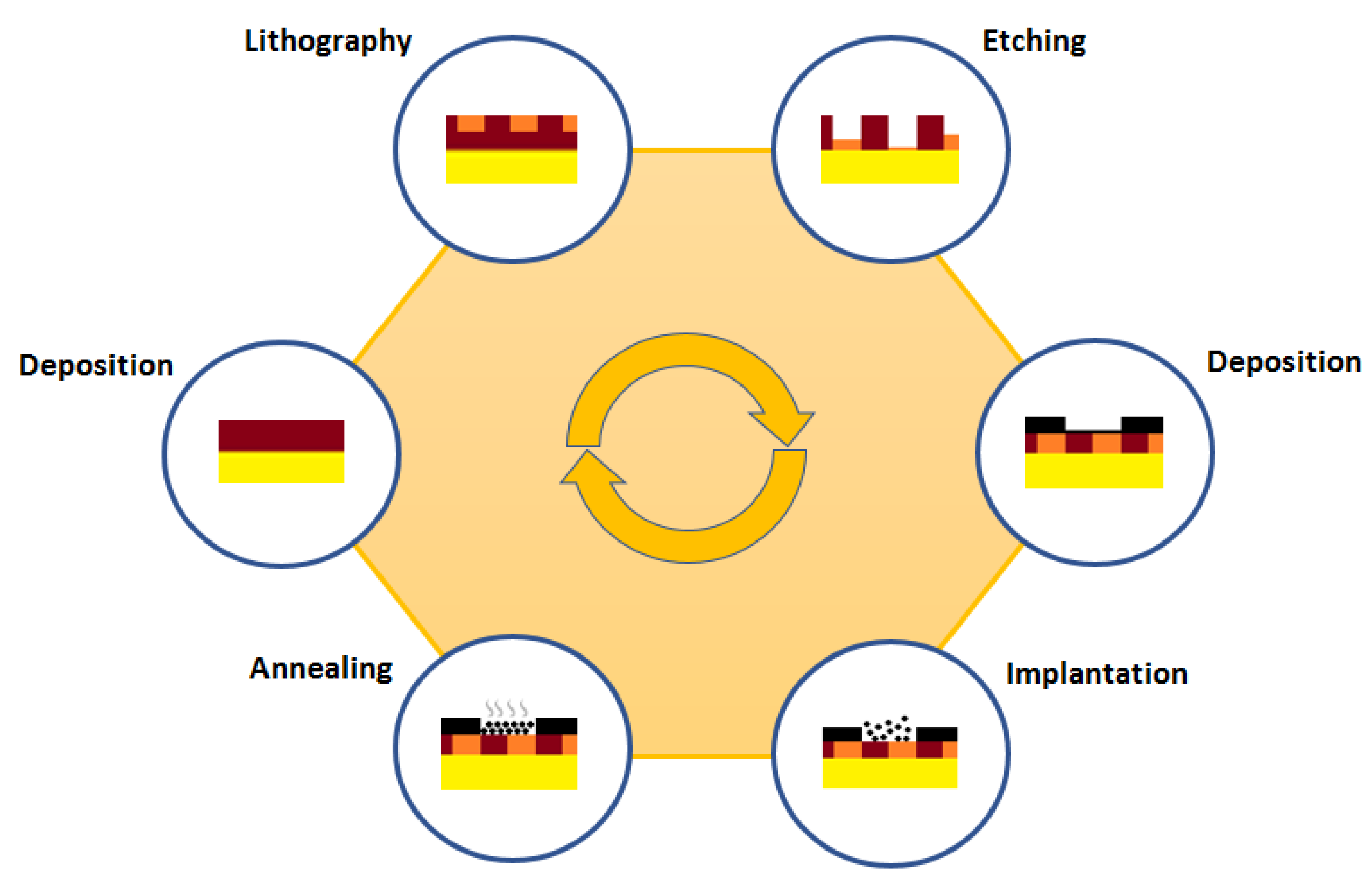
:1. Introduction
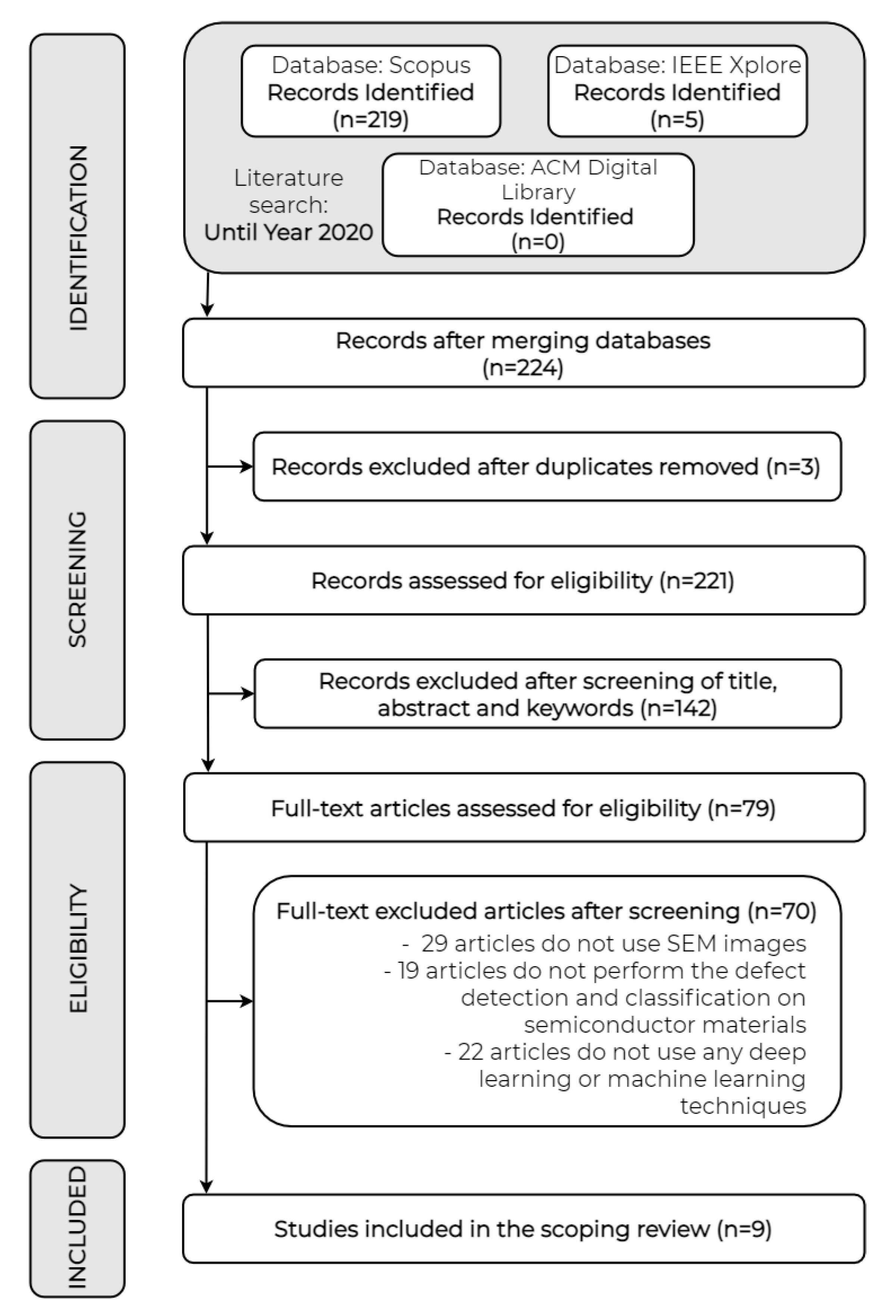
2. Search Methodology
2.1. Search Strategy
2.2. Inclusion and Exclusion Criteria
2.2.1. Inclusion Criterion
- Every publication, from inception to year 2020, that faces the semiconductor defect detection and classification task by means of a deep learning or a machine learning approach starting from a dataset composed by SEM images must be included.
2.2.2. Exclusion Criteria
- We will include just one copy per publication, removing duplicates.
- Publications that do not exclusively use SEM images in the dataset will be excluded.
- Articles that do not use any deep learning or machine learning technique will be excluded.
- Articles that do not perform the defect detection and classification task on semiconductor images will be excluded.
2.3. Refined Results Acquisition Procedure
2.4. Research Questions
- Which ML methods achieve the best performance in the detection and classification of semiconductor defects from SEM images?
- Which DL methods achieve the best performance in the detection and classification of semiconductor defects from SEM images?
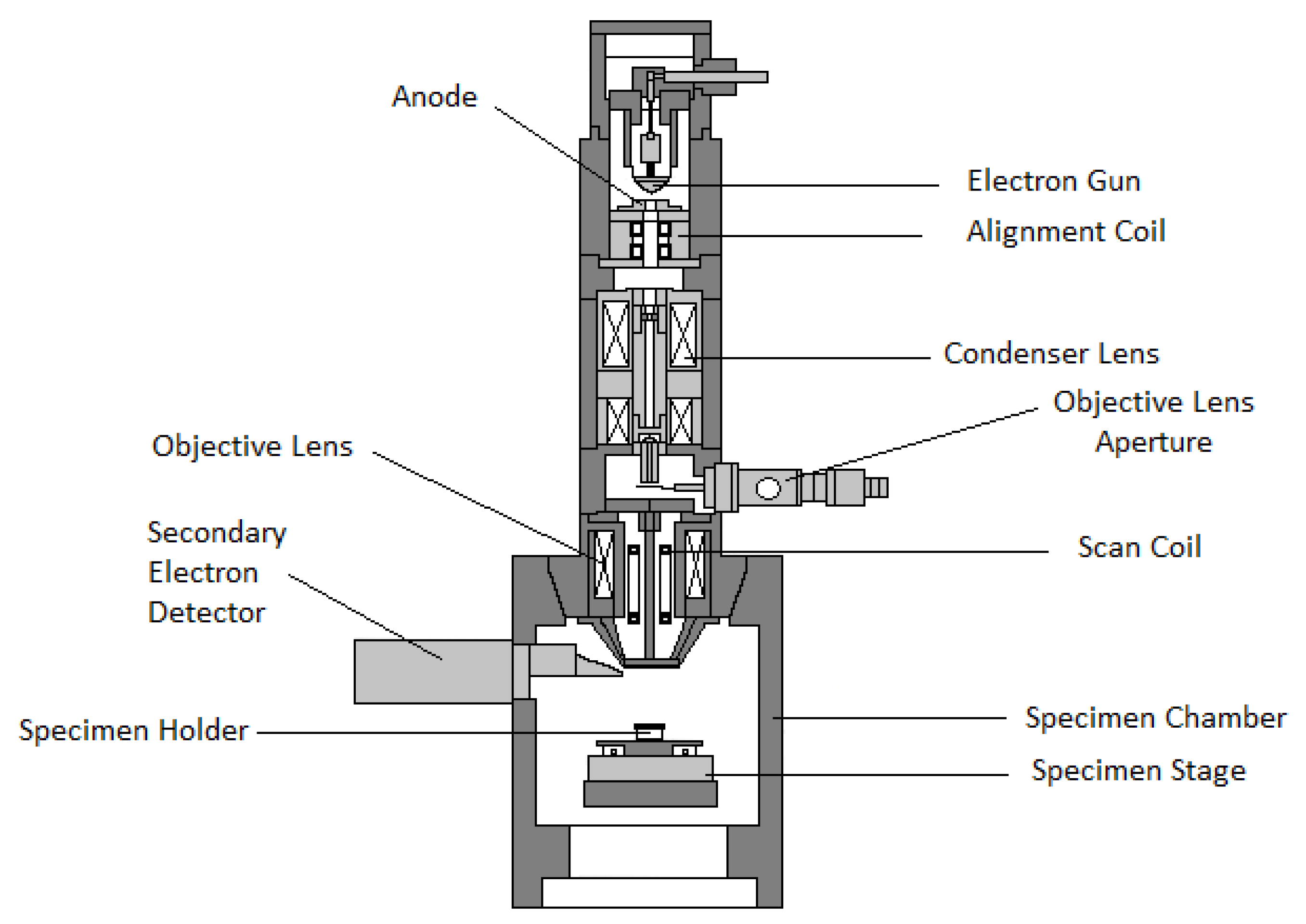
3. Scanning Electron Microscopy
Fundamentals of SEM
4. Machine Learning
4.1. Supervised Learning
4.1.1. Support Vector Machines (SVM)
4.1.2. Decision Trees (DT)
4.1.3. K-Nearest Neighbours (K-NN)
4.1.4. Naive Bayes
4.1.5. Discriminant Analysis (DA)
4.2. Unsupervised Learning
4.2.1. K-Means
4.2.2. K-Medoids
4.2.3. Self-Organising Maps (SOM)
4.3. Semi-Supervised Learning
5. Deep Learning
5.1. Elements of a CNN
5.1.1. Neurons
5.1.2. Layers
Convolutional Layers
- (1)
- Kernel size: is the first parameter that needs to be established in a convolutional layer. There is a wide range of options but, commonly, the most used sizes are , and .
- (2)
- Stride: is a parameter that defines the step size of the kernel. For example, if the stride has a value of 3, the kernel will move 3 pixels horizontally after each convolution operation. Typical values for the stride are 1, 2 and 3.
- (3)
- Depth: indicates the number of kernels that are used in each convolution. Each kernel generates a feature map, and the totality of the feature maps receives the name of feature mapping. The most used approach is to start with a few kernels along the first layers and continue increasing this number until the last convolutions.
Activation Layer
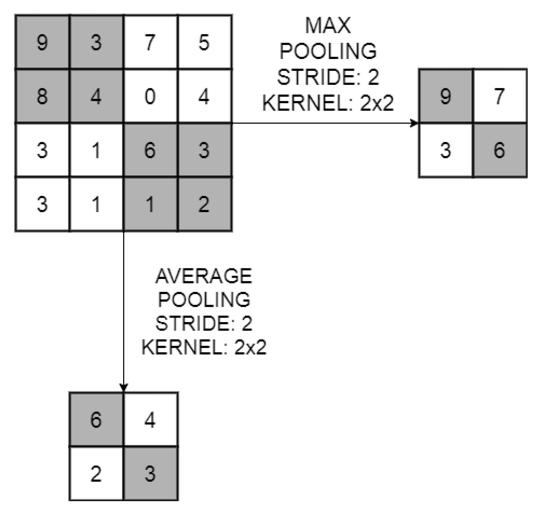
Pooling Layer
- Average pooling: offers the mean value of the sub-sampled pixels as the output value.
- Max pooling: offers the highest value of the sub-sampled pixels as the output value.
- Other methods: are not as popular as the previous ones. The reason is that they are more specific methods that offer a great performance under certain particular scenarios. Some examples are mixed pooling, stochastic pooling, spatial pyramid pooling (SPP) or region of interest pooling (ROIP).
Fully Connected Layer
Classification Layer
5.1.3. Convolutional Neural Network Models
AlexNet
VGGNet
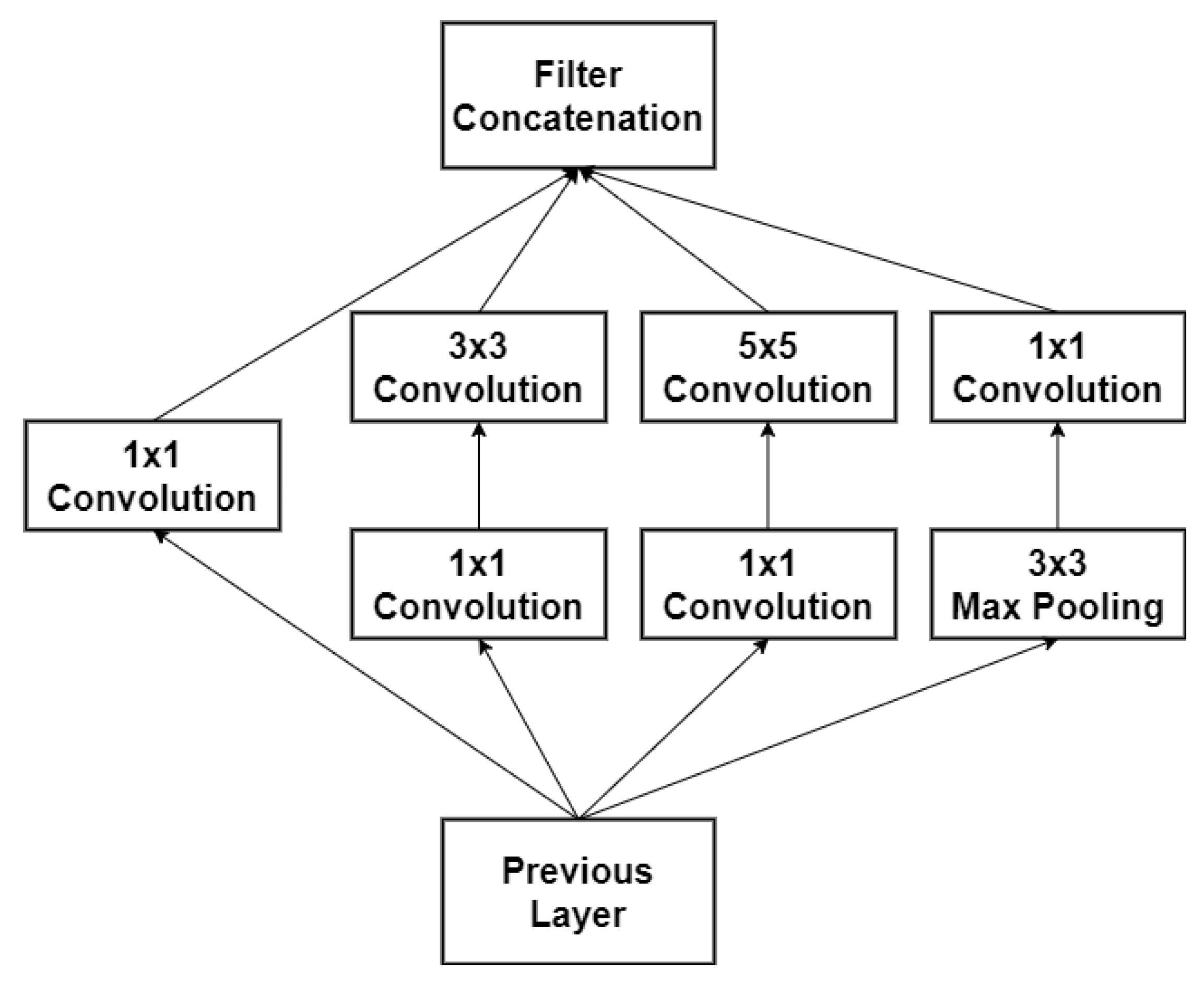
GoogleNet
ResNet
MobileNet
EfficientNet
Other Models
5.1.4. Other Configurable Parameters
Loss Functions
Optimisers
5.2. One-Stage and Two-Stage Approaches
- One-stage approaches or classification-based methods. Detection and classification (for example, of defects) is carried out simultaneously in a single stage. The main objective of the approach and its greatest advantage is the detection and classification in real-time. The disadvantage of this approach, compared to the two-stage approach, is that its accuracy is significantly lower. Therefore, it is focused on tasks that must be agile or fast and that do not require high accuracy. An example is the YOLO (You Only Look Once) architecture. YOLO can use different CNN models as a backbone such as VGGNet and GoogleNet.
- Two-stage approaches or region proposal-based methods. The detection and classification tasks are carried out separately. First, a network generates proposals of regions for object detection, and then a different network is fed with those region proposals to definitively locate and classify the object (in our particular case, the defect). Since the detection and classification task is executed in two stages, the time required to perform them is greater than in the single-stage approach. Despite this increase in time, the approach is very popular for tasks that require high accuracy. This approach can be considered for future works if, for instance, the location of the defect is not sufficiently clear. Along the first stage, the defects would be located, while in the second one they would be classified. Further information can be found in [71]. An example of this approach is region-based CNN (R-CNN) and its variants, considered one of the best architectures in terms of accuracy.
6. Results and Discussion
6.1. Article by Article Discussion
6.2. General Overview
6.3. Limitations of This Work
7. Conclusions
Author Contributions
Funding
Institutional Review Board Statement
Informed Consent Statement
Data Availability Statement
Conflicts of Interest
Abbreviations
| AE | Autoencoder |
| BCE | Binary cross-entropy |
| BSE | Back-scattered electron |
| CCE | Categorical cross-entropy |
| CCVAE | Conditional convolutional autoencoder |
| CNN | Convolutional neural network |
| DA | Discriminant analysis |
| DL | Deep learning |
| DT | Decision Tree |
| FC | Fully-connected |
| GAN | Generative adversarial network |
| GPU | Graphics processing unit |
| K-NN | K-nearest neighbours |
| LDA | Linear discriminant analysis |
| MAE | Mean absolute error |
| ML | Machine learning |
| MSE | Mean square error |
| QDA | Quadratic discriminant analysis |
| RBM | Restricted Boltzmann machine |
| ReLU | Rectifier linear unit |
| RNN | Recurrent neural network |
| ROI | Region of interest |
| SCCE | Sparse categorical cross entropy |
| SE | Secondary electron |
| SEM | Scanning electron microscope |
| SGD | Stochastic gradient descent |
| SOM | Self-organising maps |
| STEM | Scanning transmission electron microscopy |
| SVM | Support vector machine |
| VAR | Variational autoencoder |
| YOLO | You only look once |
References
- STATISTA. Monthly Semiconductor Sales Worldwide from 2012 to 2020 (in Billion U.S. Dollars); Statista GmbH: Hamburg, Germany, 2019. [Google Scholar]
- Huang, S.H.; Pan, Y.C. Automated visual inspection in the semiconductor industry: A survey. Comput. Ind. 2015, 66, 1–10. [Google Scholar] [CrossRef]
- Park, H.; Choi, J.E.; Kim, D.; Hong, S.J. Artificial Immune System for Fault Detection and Classification of Semiconductor Equipment. Electronics 2021, 10, 944. [Google Scholar] [CrossRef]
- Zheng, X.; Zheng, S.; Kong, Y.; Chen, J. Recent advances in surface defect inspection of industrial products using deep learning techniques. Int. J. Adv. Manuf. Technol. 2021, 113, 35–38. [Google Scholar] [CrossRef]
- Górriz, J.M.; Ramírez, J.; Ortíz, A.; Martínez-Murcia, F.J.; Segovia, F.; Suckling, J.; Ferrández, J.M.; Leming, M.; Zhang, Y.; Álvarez-Sánchez, J.R.; et al. Artificial intelligence within the interplay between natural and artificial computation: Advances in data science, trends and applications. Neurocomputing 2020, 410, 237–270. [Google Scholar] [CrossRef]
- O’Mahony, N.; Campbell, S.; Carvalho, A.; Harapanahalli, S.; Hernandez, G.V.; Krpalkova, L.; Riordan, D.; Walsh, J. Deep learning vs. traditional computer vision. In Science and Information Conference; Springer Nature: Cham, Switzerland, 2019; pp. 128–144. [Google Scholar]
- Abd Al Rahman, M.; Mousavi, A. A Review and Analysis of Automatic Optical Inspection and Quality Monitoring Methods in Electronics Industry. IEEE Access 2020, 8, 183192–183271. [Google Scholar] [CrossRef]
- Xiao, M.; Wang, W.; Shen, X.; Zhu, Y.; Bartos, P.; Yiliyasi, Y. Research on defect detection method of powder metallurgy gear based on machine vision. Mach. Vis. Appl. 2021, 32, 1–13. [Google Scholar] [CrossRef]
- Li, G.; Shi, J.; Luo, H.; Tang, M. A computational model of vision attention for inspection of surface quality in production line. Mach. Vis. Appl. 2013, 24, 835–844. [Google Scholar] [CrossRef]
- Schlosser, T.; Beuth, F.; Friedrich, M.; Kowerko, D. A novel visual fault detection and classification system for semiconductor manufacturing using stacked hybrid convolutional neural networks. In Proceedings of the 2019 24th IEEE International Conference on Emerging Technologies and Factory Automation (ETFA), Zaragoza, Spain, 10–13 September 2019; pp. 1511–1514. [Google Scholar]
- Sharp, M.; Ak, R.; Hedberg, T., Jr. A survey of the advancing use and development of machine learning in smart manufacturing. J. Manuf. Syst. 2018, 48, 170–179. [Google Scholar] [CrossRef]
- Tomlinson, W.; Halliday, B.; Farrington, D.; Skumanich, A. In-line SEM based ADC for advanced process control. In Proceedings of the 2000 IEEE/SEMI Advanced Semiconductor Manufacturing Conference and Workshop, Boston, MA, USA, 12–14 September 2000; pp. 131–137. [Google Scholar] [CrossRef]
- Avinun-Kalish, M.; Sagy, O.; Im, S.M.; Lee, C.; Oh, J.; Lim, J.; Yoo, H.; Kim, C. Novel SEM based imaging using secondary electron spectrometer for enhanced voltage contrast and bottom layer defect review. In Proceedings of the 2009 IEEE/SEMI Advanced Semiconductor Manufacturing Conference, Berlin, Germany, 10–12 May 2009; pp. 223–227. [Google Scholar] [CrossRef]
- Becker, B.; Porat, R.; Eschwege, H. Identification of yield loss sources in the outer dies using SEM based wafer bevel review. In Proceedings of the 2010 IEEE/SEMI Advanced Semiconductor Manufacturing Conference, San Francisco, CA, USA, 11–13 July 2010; pp. 119–122. [Google Scholar] [CrossRef]
- Newell, T.; Tillotson, B.; Pearl, H.; Miller, A. Detection of electrical defects with SEMVision in semiconductor production mode manufacturing. In Proceedings of the 2016 27th Annual SEMI Advanced Semiconductor Manufacturing Conference, Saratoga Springs, NY, USA, 16–19 May 2016; pp. 151–156. [Google Scholar] [CrossRef]
- Jain, A.; Sheridan, J.G.; Levitov, F.; Aristov, V.; Yasharzade, S.; Nguyen, H. Inline SEM imaging of buried defects using novel electron detection system. In Proceedings of the 2018 29th Annual SEMI Advanced Semiconductor Manufacturing Conference (ASMC), Saratoga Springs, NY, USA, 30 April–3 May 2018; pp. 259–263. [Google Scholar] [CrossRef]
- Zhou, W.; Apkarian, R.; Wang, Z.L.; Joy, D. Fundamentals of scanning electron microscopy (SEM). In Scanning Microscopy for Nanotechnology; Springer Nature: Cham, Switzerland, 2006; pp. 1–40. [Google Scholar] [CrossRef]
- Jain, A.; Sheridan, J.G.; Xing, R.; Levitov, F.; Yasharzade, S.; Nguyen, H. SEM imaging and automated defect analysis at advanced technology nodes. In Proceedings of the 2017 28th Annual SEMI Advanced Semiconductor Manufacturing Conference (ASMC), Saratoga Springs, NY, USA, 15–18 May 2017; pp. 240–248. [Google Scholar] [CrossRef]
- Bustillo, A.; Pimenov, D.Y.; Mia, M.; Kapłonek, W. Machine-learning for automatic prediction of flatness deviation considering the wear of the face mill teeth. J. Intell. Manuf. 2021, 32, 895–912. [Google Scholar] [CrossRef]
- Dey, A. Machine learning algorithms: A review. Int. J. Comput. Sci. Inf. Technol. 2016, 7, 1174–1179. [Google Scholar]
- Sánchez-Reolid, R.; López, M.T.; Fernández-Caballero, A. Machine Learning for Stress Detection from Electrodermal Activity: A Scoping Review. Preprints 2020. [Google Scholar] [CrossRef]
- Drucker, H.; Burges, C.J.; Kaufman, L.; Smola, A.; Vapnik, V. Support vector regression machines. Adv. Neural Inf. Process Syst. 1996, 9, 155–161. [Google Scholar]
- Cheon, S.; Lee, H.; Kim, C.O.; Lee, S.H. Convolutional neural network for wafer surface defect classification and the detection of unknown defect class. IEEE Trans. Semicond. Manuf. 2019, 32, 163–170. [Google Scholar] [CrossRef]
- Freund, Y.; Mason, L. The alternating decision tree learning algorithm. In Proceedings of the Sixteenth International Conference on Machine Learning, Bled, Slovenia, 27–30 June 1999; Volume 99, pp. 124–133. [Google Scholar]
- García-Moreno, A.I.; Alvarado-Orozco, J.M.; Ibarra-Medina, J.; Martínez-Franco, E. Ex-situ porosity classification in metallic components by laser metal deposition: A machine learning-based approach. J. Manuf. Process. 2021, 62, 523–534. [Google Scholar] [CrossRef]
- Blevins, J.; Yang, G. Machine learning enabled advanced manufacturing in nuclear engineering applications. Nucl. Eng. Des. 2020, 367, 110817. [Google Scholar] [CrossRef]
- Lei, H.; Teh, C.; Li, H.; Lee, P.H.; Fang, W. Automated Wafer Defect Classification using a Convolutional Neural Network Augmented with Distributed Computing. In Proceedings of the 2020 31st Annual SEMI Advanced Semiconductor Manufacturing Conference, Saratoga Springs, NY, USA, 24–26 August 2020; pp. 1–5. [Google Scholar] [CrossRef]
- Dudani, S.A. The distance-weighted k-nearest-neighbor rule. IEEE Trans. Syst. Man. Cybern. 1976, 6, 325–327. [Google Scholar] [CrossRef]
- Rish, I. An empirical study of the naive Bayes classifier. In Proceedings of the IJCAI 2001 Workshop on Empirical Methods in Artificial Intelligence, Seattle, DC, USA, 4–10 August 2001; Volume 3, pp. 41–46. [Google Scholar]
- Mika, S.; Ratsch, G.; Weston, J.; Scholkopf, B.; Mullers, K.R. Fisher discriminant analysis with kernels. In Proceedings of the Neural Networks for Signal Processing IX, Madison, WI, USA, 25–25 August 1999; pp. 41–48. [Google Scholar] [CrossRef]
- Singh, A.; Thakur, N.; Sharma, A. A review of supervised machine learning algorithms. In Proceedings of the 2016 3rd International Conference on Computing for Sustainable Global Development, New Delhi, India, 16–18 March 2016; pp. 1310–1315. [Google Scholar]
- Hartigan, J.A.; Wong, M.A. Algorithm AS 136: A k-means clustering algorithm. J. R. Stat. Soc. C 1979, 28, 100–108. [Google Scholar] [CrossRef]
- Halder, S.; Cerbu, D.; Saib, M.; Leray, P. SEM image analysis with K-means algorithm. In Proceedings of the 2018 29th Annual SEMI Advanced Semiconductor Manufacturing Conference, Saratoga Springs, NY, USA, 30 April–3 May 2018; pp. 255–258. [Google Scholar] [CrossRef]
- Kaufman, L.; Rousseeuw, P.J. Partitioning Around Medoids (Program PAM). In Finding Groups in Data: An Introduction to Cluster Analysis; Wiley: New York, NY, USA, 1990; pp. 68–125. [Google Scholar] [CrossRef]
- Kohonen, T. The self-organizing map. Proc. IEEE 1990, 78, 1464–1480. [Google Scholar] [CrossRef]
- Chang, C.Y.; Li, C.; Chang, J.W.; Jeng, M. An unsupervised neural network approach for automatic semiconductor wafer defect inspection. Expert Syst. Appl. 2009, 36, 950–958. [Google Scholar] [CrossRef]
- Guo, Y.; Liu, Y.; Oerlemans, A.; Lao, S.; Wu, S.; Lew, M.S. Deep learning for visual understanding: A review. Neurocomputing 2016, 187, 27–48. [Google Scholar] [CrossRef]
- Mery, D. Aluminum Casting Inspection using Deep Object Detection Methods and Simulated Ellipsoidal Defects. Mach. Vis. Appl. 2021, 32, 1–16. [Google Scholar] [CrossRef]
- Wang, J.; Ma, Y.; Zhang, L.; Gao, R.X.; Wu, D. Deep learning for smart manufacturing: Methods and applications. J. Manuf. Syst. 2018, 48, 144–156. [Google Scholar] [CrossRef]
- Lei, C.W.; Zhang, L.; Tai, T.M.; Tsai, C.C.; Hwang, W.J.; Jhang, Y.J. Automated Surface Defect Inspection Based on Autoencoders and Fully Convolutional Neural Networks. Appl. Sci. 2021, 11, 7838. [Google Scholar] [CrossRef]
- Fukushima, K. Neocognitron: A hierarchical neural network capable of visual pattern recognition. Neural Netw. 1988, 1, 119–130. [Google Scholar] [CrossRef]
- Albawi, S.; Mohammed, T.A.; Al-Zawi, S. Understanding of a convolutional neural network. In Proceedings of the 2017 International Conference on Engineering and Technology, Antalya, Turkey, 21–23 August 2017; pp. 1–6. [Google Scholar] [CrossRef]
- Zhang, Z.; Wen, G.; Chen, S. Weld image deep learning-based on-line defects detection using convolutional neural networks for Al alloy in robotic arc welding. J. Manuf. Process. 2019, 45, 208–216. [Google Scholar] [CrossRef]
- Khodja, A.Y.; Guersi, N.; Saadi, M.N.; Boutasseta, N. Rolling element bearing fault diagnosis for rotating machinery using vibration spectrum imaging and convolutional neural networks. Int. J. Adv. Manuf. Technol. 2020, 106, 1737–1751. [Google Scholar] [CrossRef]
- Xia, C.; Pan, Z.; Fei, Z.; Zhang, S.; Li, H. Vision based defects detection for Keyhole TIG welding using deep learning with visual explanation. J. Manuf. Process. 2020, 56, 845–855. [Google Scholar] [CrossRef]
- Wang, J.; Lee, S. Data Augmentation Methods Applying Grayscale Images for Convolutional Neural Networks in Machine Vision. Appl. Sci. 2021, 11, 6721. [Google Scholar] [CrossRef]
- Goodfellow, I.; Pouget-Abadie, J.; Mirza, M.; Xu, B.; Warde-Farley, D.; Ozair, S.; Bengio, Y.; Courville, A. Generative adversarial nets. Adv. Neural Inf. Process. Syst. 2014, 27, 2672–2680. [Google Scholar]
- Yun, J.P.; Shin, W.C.; Koo, G.; Kim, M.S.; Lee, C.; Lee, S.J. Automated defect inspection system for metal surfaces based on deep learning and data augmentation. J. Manuf. Syst. 2020, 55, 317–324. [Google Scholar] [CrossRef]
- Tran, M.Q.; Liu, M.K.; Tran, Q.V. Milling chatter detection using scalogram and deep convolutional neural network. Int. J. Adv. Manuf. Technol. 2020, 107, 1505–1516. [Google Scholar] [CrossRef]
- Han, J.; Zhang, D.; Cheng, G.; Liu, N.; Xu, D. Advanced deep-learning techniques for salient and category-specific object detection: A survey. IEEE Signal Process. Mag. 2018, 35, 84–100. [Google Scholar] [CrossRef]
- Nguyen, T.P.; Choi, S.; Park, S.J.; Park, S.H.; Yoon, J. Inspecting method for defective casting products with convolutional neural network (CNN). Int. J. Precis. Eng.-Manuf.-Green Technol. 2021, 8, 583–594. [Google Scholar] [CrossRef]
- Dhillon, A.; Verma, G.K. Convolutional neural network: A review of models, methodologies and applications to object detection. Prog. Artif. Intell. 2020, 9, 85–112. [Google Scholar] [CrossRef]
- Krizhevsky, A.; Sutskever, I.; Hinton, G.E. Imagenet classification with deep convolutional neural networks. Commun. ACM 2017, 60, 84–90. [Google Scholar] [CrossRef]
- Simonyan, K.; Zisserman, A. Very deep convolutional networks for large-scale image recognition. arXiv 2014, arXiv:1409.1556. [Google Scholar]
- Yuan-Fu, Y.; Min, S. Double Feature Extraction Method for Wafer Map Classification Based on Convolution Neural Network. In Proceedings of the 2020 31st Annual SEMI Advanced Semiconductor Manufacturing Conference, Saratoga Springs, NY, USA, 24–26 August 2020; pp. 1–6. [Google Scholar] [CrossRef]
- O’Leary, J.; Sawlani, K.; Mesbah, A. Deep Learning for Classification of the Chemical Composition of Particle Defects on Semiconductor Wafers. IEEE Trans. Semicond. Manuf. 2020, 33, 72–85. [Google Scholar] [CrossRef]
- Szegedy, C.; Liu, W.; Jia, Y.; Sermanet, P.; Reed, S.; Anguelov, D.; Erhan, D.; Vanhoucke, V.; Rabinovich, A. Going deeper with convolutions. In Proceedings of the IEEE Conference on Computer Vision and Pattern Recognition, Boston, MA, USA, 7–12 June 2015; pp. 1–9. [Google Scholar] [CrossRef] [Green Version]
- Imoto, K.; Nakai, T.; Ike, T.; Haruki, K.; Sato, Y. A CNN-based transfer learning method for defect classification in semiconductor manufacturing. In Proceedings of the 2018 International Symposium on Semiconductor Manufacturing, Tokyo, Japan, 10–11 December 2018; pp. 1–3. [Google Scholar] [CrossRef]
- Monno, S.; Kamada, Y.; Miwa, H.; Ashida, K.; Kaneko, T. Detection of Defects on SiC Substrate by SEM and Classification Using Deep Learning. In International Conference on Intelligent Networking and Collaborative Systems; Springer Nature Switzerland AG: Cham, Switzerland, 2018; pp. 47–58. [Google Scholar] [CrossRef]
- He, K.; Zhang, X.; Ren, S.; Sun, J. Deep residual learning for image recognition. In Proceedings of the IEEE Conference on Computer Vision and Pattern Recognition, Las Vegas, NV, USA, 27–30 June 2016; pp. 770–778. [Google Scholar] [CrossRef] [Green Version]
- Howard, A.G.; Zhu, M.; Chen, B.; Kalenichenko, D.; Wang, W.; Weyand, T.; Andreetto, M.; Adam, H. Mobilenets: Efficient convolutional neural networks for mobile vision applications. arXiv 2017, arXiv:1704.04861. [Google Scholar]
- Tan, M.; Le, Q. Efficientnet: Rethinking model scaling for convolutional neural networks. In Proceedings of the International Conference on Machine Learning, Long Beach, CA, USA, 9–15 June 2019; pp. 6105–6114. [Google Scholar]
- Sandler, M.; Howard, A.; Zhu, M.; Zhmoginov, A.; Chen, L.C. Mobilenetv2: Inverted residuals and linear bottlenecks. In Proceedings of the IEEE Conference on Computer Vision and Pattern Recognition, Salt Lake City, UT, USA, 18–23 June 2018; pp. 4510–4520. [Google Scholar]
- Su, C.T.; Yang, T.; Ke, C.M. A neural-network approach for semiconductor wafer post-sawing inspection. IEEE Trans. Semicond. Manuf. 2002, 15, 260–266. [Google Scholar] [CrossRef]
- Choi, D.; Shallue, C.J.; Nado, Z.; Lee, J.; Maddison, C.J.; Dahl, G.E. On empirical comparisons of optimizers for deep learning. arXiv 2019, arXiv:1910.05446. [Google Scholar]
- Robbins, H.; Monro, S. A stochastic approximation method. Ann. Math. Stat. 1951, 22, 400–407. [Google Scholar] [CrossRef]
- Polyak, B.T. Some methods of speeding up the convergence of iteration methods. USSR Comput. Math. Math. Phys. 1964, 4, 1–17. [Google Scholar] [CrossRef]
- Nesterov, Y.E. A method for solving the convex programming problem with convergence rate O (1/k2). Dokl. Akad. Nauk SSSR 1983, 269, 543–547. [Google Scholar]
- Tieleman, T.; Hinton, G. Lecture 6.5-rmsprop: Divide the gradient by a running average of its recent magnitude. COURSERA Neural Netw. Mach. Learn. 2012, 4, 26–31. [Google Scholar]
- Kingma, D.P.; Ba, J. Adam: A method for stochastic optimization. arXiv 2014, arXiv:1412.6980. [Google Scholar]
- Miao, R.; Jiang, Z.; Zhou, Q.; Wu, Y.; Gao, Y.; Zhang, J.; Jiang, Z. Online inspection of narrow overlap weld quality using two-stage convolution neural network image recognition. Mach. Vis. Appl. 2021, 32, 27. [Google Scholar] [CrossRef]


| Search Term | Description |
|---|---|
| defect OR flaw OR imperfection OR fault OR crack OR bug OR deficiency | Synonyms for defect |
| detection OR detecting OR recognition OR recognising OR identification OR identifying | Synonyms for detection |
| classification OR classifying OR categorising OR categorisation | Synonyms for classification |
| vision OR visual OR image | Screening the articles which work with visual detection |
| wafer OR semiconductor | Seeking articles in which the defects appear in semiconductor wafers |
| SEM OR “scanning electron microscope” OR “scanning electron microscopy” | Articles with SEM as inspection device |
| ”deep learning” OR “machine learning” | Articles in which defects are classified using these techniques |
| Reference | Method | Accuracy |
|---|---|---|
| CNN (self design) | 0.962 | |
| [23] | SVM (radial basis function) | 0.925 |
| K-NN | 0.933 | |
| [27] | CNN (self design) | 0.953 |
| Random forest | 0.942 | |
| [33] | K-means | — |
| [36] | SOM | * |
| Inception V2 | 0.900 | |
| ResNet 50 | 0.875 | |
| [55] | VGGNet16 | 0.844 |
| R-Inception V2 | 0.974 | |
| R-ResNet 50 | 0.968 | |
| R-VGGNet16 | 0.960 | |
| [56] | CNN (self design) | 0.821 |
| [58] | Inception V1 | 0.873 |
| Commercial ADC | 0.772 | |
| [59] | Inception V2 | 0.600 |
| ResNet 50 | 0.700 | |
| CNN Back-propagation | 1 | |
| [64] | CNN Linear Vector Quantisation | 1 |
| CNN Radial Basis Function | 0.900 |
Publisher’s Note: MDPI stays neutral with regard to jurisdictional claims in published maps and institutional affiliations. |
© 2021 by the authors. Licensee MDPI, Basel, Switzerland. This article is an open access article distributed under the terms and conditions of the Creative Commons Attribution (CC BY) license (https://creativecommons.org/licenses/by/4.0/).
Share and Cite
López de la Rosa, F.; Sánchez-Reolid, R.; Gómez-Sirvent, J.L.; Morales, R.; Fernández-Caballero, A. A Review on Machine and Deep Learning for Semiconductor Defect Classification in Scanning Electron Microscope Images. Appl. Sci. 2021, 11, 9508. https://doi.org/10.3390/app11209508
López de la Rosa F, Sánchez-Reolid R, Gómez-Sirvent JL, Morales R, Fernández-Caballero A. A Review on Machine and Deep Learning for Semiconductor Defect Classification in Scanning Electron Microscope Images. Applied Sciences. 2021; 11(20):9508. https://doi.org/10.3390/app11209508
Chicago/Turabian StyleLópez de la Rosa, Francisco, Roberto Sánchez-Reolid, José L. Gómez-Sirvent, Rafael Morales, and Antonio Fernández-Caballero. 2021. "A Review on Machine and Deep Learning for Semiconductor Defect Classification in Scanning Electron Microscope Images" Applied Sciences 11, no. 20: 9508. https://doi.org/10.3390/app11209508