1. Introduction
A number of unique properties of nanodiamonds make them attractive for a variety of industrial and biomedical applications [
1,
2,
3,
4]. The mass production of nanodiamond particles is currently carried out by two methods: (i) detonation of high explosives with high carbon content [
5,
6] and (ii) milling micrometer-sized diamond particles [
7] produced while using hydraulic presses at high pressure and high temperature [
8]. Detonation nanodiamonds and high-pressure high-temperature (HP-HT) nanodiamonds both have a wide variety of impurities [
5,
9,
10,
11]. More than 60 elements are known to be present in diamonds according to analytical data, but only a few of them, namely nitrogen, boron, nickel, silicon, and hydrogen, can form intrinsic structural defects [
12]. These impurities and vacancies affect the optical properties of nanodiamonds, such as absorption and luminescence.
HP-HT nanodiamonds contain substitutional nitrogen impurities with a concentration of about 100–300 ppm [
11,
13]. These substitutional nitrogen impurity atoms form stable complexes with vacancies (or other impurity atoms), leading to the formation of optically active defect centers. Among these are the well-studied nitrogen-vacancy [N-V] (having both neutral [N-V]
0 and negatively charged [N-V]
− forms), consisting of one nitrogen atom [N] in a substitutional position and one vacancy [V] [
14]. These complexes have a high probability of electronic transitions [
15]. HP-HT nanodiamonds grown while using nickel or a nickel alloy as a catalyst contain a number of nickel related optical centers [
16,
17]. The absorption and luminescence spectra of the HP-HT nanodiamonds grown in the Fe-Ni-C system exhibit a large number of absorption lines in a wide spectral region (300–900 nm) belonging to [Ni]- [
16,
18] and [Ni-N]- [
19,
20] centers. The defect centers listed above, as well as other impurity centers formed during the synthesis of HP-HT nanodiamonds, can affect the material response to laser irradiation.
It is known that focused laser radiation can initiate processes that lead to laser modification of nanodiamonds. A large number of studies have demonstrated laser modification of the surface of single and polycrystalline diamonds, nanocrystalline diamond films, ultra-thin diamond-like carbon, amorphous diamond-like films, and tetrahedral amorphous carbon while using powerful nanosecond, picosecond, and femtosecond lasers operating in the ultraviolet, visible, and infrared ranges [
21,
22,
23,
24,
25,
26,
27,
28]. In these studies, laser microstructuring occurs as a result of local graphitization of the surface due to single- or multi-photon absorption (depending on the laser quantum energy) of powerful laser radiation, which causes the ionization of the sp
3-carbon material.
Recently, we have demonstrated the possibility of blackening and microstructuring of semitransparent detonation nanodiamond films upon low-power focused He-Ne laser irradiation at 633 nm [
29]. Such modification of the nanodiamond films can be used in order to fabricate optical structures designed on a micro-scale. Briefly, we have also demonstrated that cw He-Ne laser at a wavelength of 633 nm causes the transformation of HP-HT nanodiamonds into sp
2-carbon (blackening) [
30]. In the current paper, we have studied this phenomenon accompanied by green luminescence in more detail, which allows for us to establish a link between film blackening and the local presence of Ni-related photoluminescent centers.
2. Materials and Methods
The HP-HT nanodiamond particles with an average size of 150 nm were sourced from the vendor (Diamond Innovations, Worthington, OH, USA) and then dispersed in deionized water [
30]. 20-µm-thick (see
Figure 1a) and 0.5 µm-thick films were obtained by dropping the HP-HT nanodiamond aqueous suspension on a quartz substrate and then drying it at room temperature. The 0.5-µm-thick films were used to study the extinction spectrum. The main experiments on laser modification were carried out with the 20-μm-thick films. X-ray diffraction (XRD), Raman spectroscopy, atomic force microscopy (AFM), and scanning electron microscopy (SEM) were used to characterize the films and HP-HT nanodiamonds under study. HP-HT nanodiamond films are insulating; therefore, to eliminate the effect of charge accumulation on the surface in the course of examination with a scanning electron microscope, the surfaces of the films were sputtered with a thin layer of gold with a thickness of about 20 nm.
A D2 PHASER diffractometer from Bruker was used to study the XRD patterns of nanodiamonds. A copper-based X-ray tube that generates radiation at wavelengths λ1 (Kα1 line) = 0.1541 nm, λ2 (Kα2 line) = 0.1544 nm, and λ3 (Kβ line) = 0.1392 nm is used in the diffractometer. For the spectral separation of the Kα line, an X-ray filter from a nickel plate that attenuates radiation at a wavelength of λ3 is used. The Kα1 and Kα2 emission lines are a doublet; therefore, their spectral separation from each other using a nickel filter is not possible. However, the intensity of the Kα2 spectral line is approximately two times lower than the intensity of the Kα1 line. Thus, the diffraction lines of Kα1 copper radiation should be noticeable in the X-ray diffraction pattern of the material under study.
The HP-HT nanodiamond powder obtained from the suspension was placed on a glass substrate to record XRD patterns. The XRD pattern of the substrate without powder was recorded separately. Then, to obtain a true diffraction pattern of the powder, the corresponding subtraction of the data of two experiments was carried out.
Figure 2 shows the diffraction pattern of the HP-HT nanodiamonds. One can see that, in the range of the angle 2θ from 25 to 100°, the pattern contains three large peaks and one small peak. Large peaks at 2θ angles of 43.9, 75.3 and 91.5° correspond to X-ray diffraction Кα on the {111}, {220}, {311} planes of diamond crystallites with interplanar distances
d111 = 0.2060 nm,
d220 = 0.1261 nm, and
d311 = 0.1075 nm, respectively, where the subscripts denote the crystallographic plane, according to the Powder Diffraction File (PDF) 00-006-0675 (see
Figure 2 lower part). The weak peak at an angle of 2θ = 39.5° is due to the diffraction of the weak CuKβ radiation line on the {111} planes. Thus, X-ray diffraction confirms that the sample under study is a high-quality diamond material.
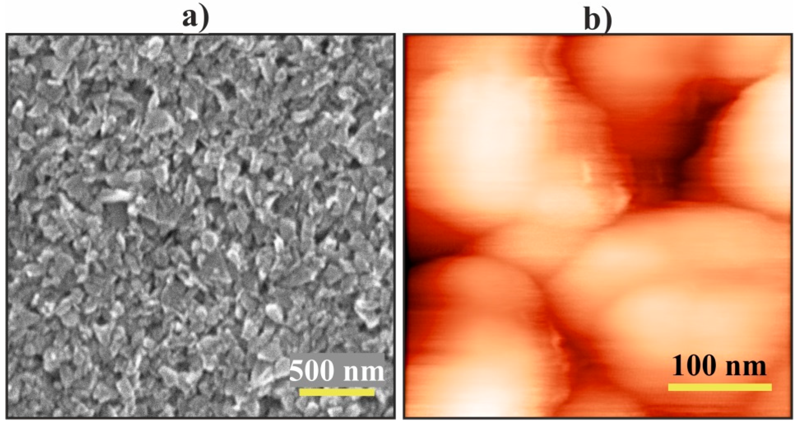
Figure 3a presents the scanning electron microscope Inspect S50 image of the film under study.
Figure 3b illustrates the typical morphology of the same film, measured with an atomic force microscope SOLVER 47 PRO. The images show that the film surface has a granular structure, with a characteristic size of the observed particles of about 150 nm.
The extinction spectrum of the HP-HT nanodiamond film with a thickness of 0.5 µm shows the maximum at the wavelength of 208 nm, corresponding to the photon energy of 5.96 eV (
Figure 4a). This absorption band corresponds to the transition from the valence band to the conduction band of a diamond.
Figure 4a also shows monotonically decreasing extinction of the film due to decreasing Rayleigh scattering by nanoparticles and film inhomogeneities with the increase in the wavelength.
The luminescence spectra of an aqueous suspension of HP-HT nanodiamonds were studied while using the LS55 luminescence spectrophotometer (Perkin Elmer). It allows for changing the wavelength of the exciting radiation using the excitation monochromator in the range from 200 to 800 nm. The spectral range of the emission monochromator spans from 200 to 900 nm. The luminescence intensity of the suspension was recorded, depending on the wavelength of the exciting radiation using a photomultiplier installed at the output of the emission monochromator. When recording the luminescence spectra, the slit widths of both monochromators were equal and set to 5 nm. At the input of the emission monochromator, various optical filters significantly suppressing the exciting radiation were installed in order to reduce its influence on the luminescence spectra.
Figure 4b,c illustrate the luminescence spectra recorded in the Stokes region at excitation radiation wavelengths λ
ex = 220, 320, 400, and 420 nm. It can be seen that when the wavelength λ
ex is changed, the luminescence spectrum changes too. However, in all recorded spectra, there are peaks that are common to all excitation wavelengths λ
ex. These are the peaks that correspond to the wavelengths of 461, 485, and 529 nm.
Figure 4d shows the luminescence spectra recorded in the anti-Stokes region when excited by radiation at wavelengths λ
ex = 633 and 650 nm. This spectrum clearly shows up-conversion luminescence bands in the blue (461–490 nm) and green (510–535 nm) wavelength regions. It is noteworthy that, in the blue and green regions of the optical spectrum, there are peaks at 485 and 528 nm, respectively, which were observed when luminescence was excited by radiation at λ
ex = 220, 300, and 360 nm. Note that all of the spectra in
Figure 4b–d are identical to that of the HP-HT nanodiamond film presented in
Figure 1a.
Experiments on the laser modification of HP-HT nanodiamond films and the study of their Raman spectra were carried out at the wavelength of 633 nm while using Horiba HR800 Raman spectrometer with a He-Ne excitation source. In this case, the laser radiation could be focused on the surface of the film using interchangeable objectives with a magnification of 10 (10×), 50 (50×), or 100 (100×). The laser beam diameters (at a level of 1/e
2) in the focal plane of the objectives were measured by scanning laser beam profilometer BC 106-VIS (ThorLabs) along the laser beam axis [
31]. The diameters of the waist of a laser beam focused with 10×, 50×, and 100× objectives were 20.7, 7.4, and 4.1 μm, respectively. The measurements carried out with a calibrated photodetector showed that the maximum laser power at a 100 × objective output is 8.4 mW. Thus, the maximum light intensity did not exceed 65 kW/cm
2. The Raman spectra of the films under study were measured at the intensity of 5.4 kW/cm
2.
In the experiments on laser modification, the HP-HT nanodiamond film with a thickness of 20 µm on a quartz substrate was moving relative to the laser beam waist while using the coordinate table (see
Figure 5a). One can see the photo of the HP-HT nanodiamond film that was irradiated step-by-step over the entire surface area presented in
Figure 1b. The emission from the film during laser treatment was recorded while using a photo camera (see
Figure 5d) after passing through a glass filter. The color glass filter was used to weaken the radiation at 633 nm, reflected from the film.
Figure 5b shows the transmission spectrum of this glass filter.
3. Results
It was found that at the threshold laser intensity of 33 kW/cm
2 the HP-HT nanodiamond film surface can start blackening in the laser beam waist area both in ambient and Ar atmospheres. When the film and the focused beam move relative to each other at a low speed (about 0.1 mm/s), blackening ight start in some areas of the film. During irradiation of spots on the stationary film blackening typically does not occur. In other words, there are areas where neither green emission generation nor blackening occurs under the laser radiation of even higher than 33 kW/cm
2 (up to 65 kW/cm
2) intensity. These areas are clearly visible in
Figure 1b as white regions. Therefore, it is much easier to get the film blackened moving it relative to the laser beam (i.e. producing a line) than irradiating the motionless film at a single point. Numerous experiments have shown that a stationary film can also be blackened, depending on the region of the film. However, the probability of finding such a region is quite low. The use of 10× and 50× objectives, which provided maximum power densities of 3 and 20 kW/cm
2, respectively, did not lead to blackening, as the power densities were lower than the threshold of laser blackening (33 kW/cm
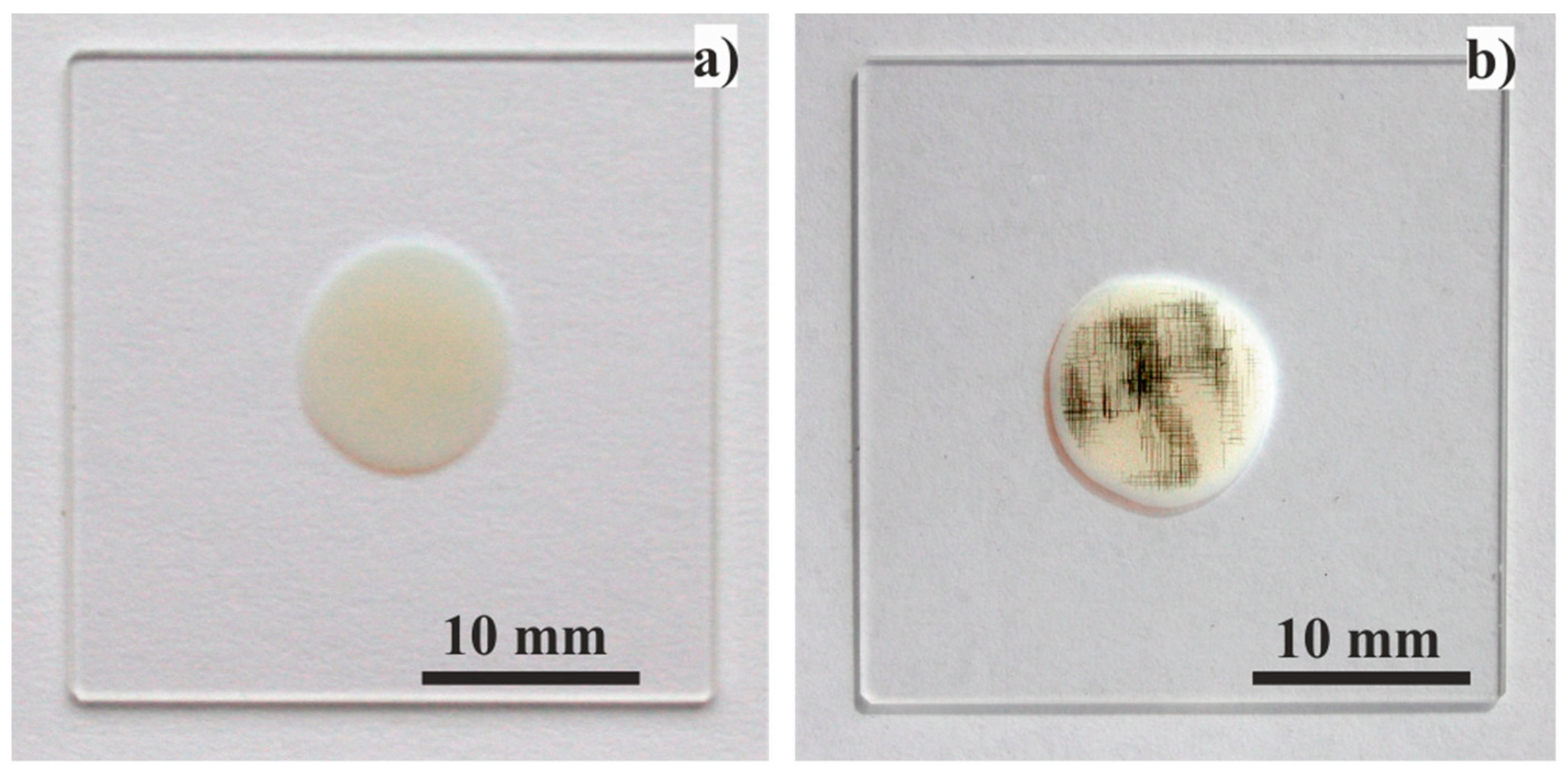
2). It should also be noted that blackening did not occur on the film with a thickness of 0.5 µm at maximum intensity, whether it was moving or stationary. One can see a line, a square, and a triangle “written” on the surface of the 20 µm thick film in
Figure 6. The optical images in
Figure 6 were obtained while using a microscope and a camera incorporated into a Raman spectrometer. It can be seen that the width of the blackened segments in the transverse direction is about 5 μm, which is slightly larger than the diameter of the laser beam waist (4.1 μm). The blackening of the film was shown to be accompanied by green emission by visual observation through a glass filter of the laser irradiated area (
Figure 5a). One can see the red spot of the reflected laser in that area when
P = 5.4 kW/cm
2 and blackening of the film does not occur, and green emission at
P = 65 kW/cm
2m accompanied by the film blackening in
Figure 5c,d. Note that that the observed green emission is a one-time event for the irradiated area, i.e. no emission is observed after blackening the film area.
Figure 7a shows the optical transmittance of the blackened region of the film at a wavelength of 633 nm, depending on its coordinate along the
x-axis perpendicular to the
y-axis, which is parallel to the symmetry axis of the blackened line (see
Figure 7d). The presented dependence was obtained using a photodetector, the photosensitive part of which with the diameter of 1 cm was placed in the immediate vicinity of the film while the film and the focused beam move relative to each other (100×). The transmittance of the film is shown to be significantly decreased after laser exposure.
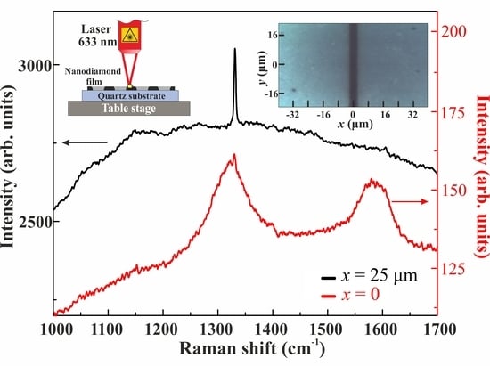
Figure 7b shows the Raman spectra that were obtained for non-blackened and blackened regions of the film at an intensity of 5.4 kW/cm
2 using a 100× objective. One can see a strong Raman signal with a frequency shift of 1331 cm
−1, slightly different from that of a bulk crystalline diamond [
32], in the spectrum of a non-blackened region (
Figure 7b, black curve). Note that, depending on the wavelength of the pumping laser and the nanoparticle mean size, the Raman shifts of detonation nanodiamonds, CVD nanodiamonds, and HP-HT nanodiamonds are known to be in the range of 1325–1332 cm
−1 [
33,
34,
35,
36,
37,
38]. In the Raman spectrum of a blackened region, there is no diamond signal (see
Figure 7b, red curve), but there are two distinct broad Raman lines with frequency shifts of maximums of 1320 and 1580 cm
−1, typical for sp
2-carbon.
Figure 7c shows the dependence of Raman peak intensity of the HP-HT nanodiamond on
x coordinate. The HP-HT nanodiamond Raman peak intensity is mirror-symmetric about
x = 0 in the first approximation.
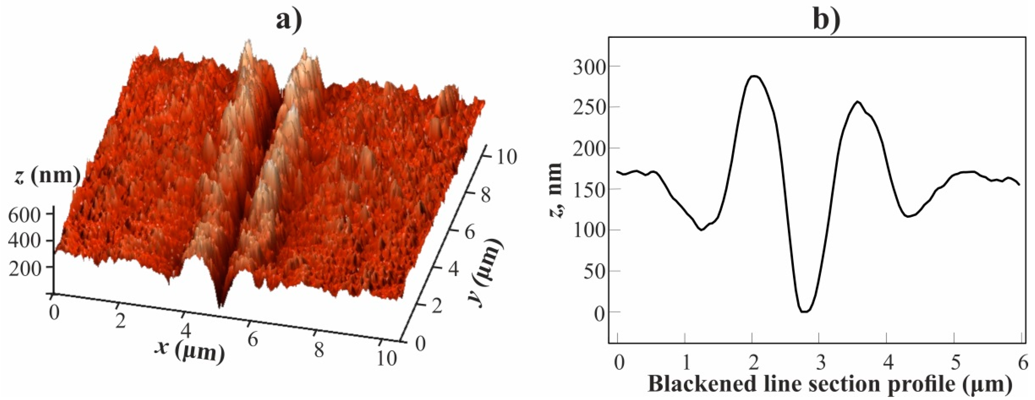
Figure 8a shows a three-dimensional (3D) image of a blackened line segment obtained while using the atomic force microscope. It can be seen that the blackened area is a notch, on both sides of which, there are parallel formations in the form of a ridge, raised above the average level of the film surface. The depth of the notch and the height of the shaft are about 150 and 100 nm, respectively (see
Figure 8b).
Figure 9a shows an image of a blackened line segment obtained while using a scanning electron microscope in the mode of secondary electrons detection. The notch located along the line of laser exposure is clearly visible. Its width in the transverse direction is 3.2 µm, which roughly coincides with the width of the notch presented in the AFM image (see
Figure 8). In addition, it can be seen that the zone of laser irradiation extends in the form of two parallel dark stripes with unmodified surface relief along the notch on both its sides. As a result, the width of the laser irradiation zone along the axis perpendicular to the direction of movement of the focused laser beam reaches 18-20 μm, which is significantly larger than the laser beam waist diameter.
Figure 9b shows the SEM image of the area that is located at the bottom of the laser-induced notch shown in
Figure 9a. It can be seen that the granularity of the film surface is noticeably reduced after laser modification.
The experiments have shown that blackening and green emission are unlikely to occur when the film is stationary. In addition to visual observation, this is confirmed by Raman spectra of the same point on a fixed film.
Figure 10a shows the Raman spectra of the film recorded at a randomly chosen area, which was irradiated for intervals of time Δ
t = 0.5, 10 and 120 min. by 65 kW/cm
2 laser radiation. The spectra were measured after Δ
t irradiation time at 65 kW/cm
2. It can be seen that the presented spectra have a broad luminescence band in the spectral range of 650–700 nm and one sharp diamond peak with a frequency shift of about 1331 cm
−1.
Figure 10b depicts HP-HT nanodiamond Raman peak intensity and its shift in a randomly chosen area of the stationary film as a function of laser exposure time at 65 kW/cm
2.
Figure 10c shows fitted HP-HT nanodiamond Raman peaks for the film point irradiated for Δ
t = 0.5 and 120 min.
Figure 10b,c demonstrate that an increase in the duration of laser irradiation Δ
t does not lead to a noticeable change in the Raman intensity and shift of the HP-HT nanodiamond peak. At the same time, the decrease in the luminescence intensity in a wide spectral range is clearly observed, i.e. the longer the film is irradiated, the lower the luminescence intensity at wavelengths in the spectral range of 650–700 nm (see
Figure 10d). It should be emphasized that, during the lengthy experiment, the results of which are shown in
Figure 10a, laser-induced blackening of the film did not occur and the green emission was not observed.
Thus, the transformation of HP-HT nanodiamond particles into sp
2-carbon, which is accompanied by a green emission, can occur in some areas of the film during its movement relative to a laser beam spot with an intensity of more than 33 kW/cm
2. The partial graphitization of HP-HT nanodiamond particles also happens in the area near and several times larger than the beam waist. In addition to the dependence that is shown in
Figure 7c, this is indicated by dark parallel bands with a width from edge to edge equal to 18–20 μm, appearing on the SEM image (see
Figure 9). It is obvious that these dark bands in the SEM image arise from the increase of the HP-HT nanodiamond film electrical conductivity due to the formation of sp
2-carbon.
4. Discussion
The structural transformation of sp
3- to sp
2-carbon was previously observed by Osswald et al. [
39] while irradiating powders of detonation nanodiamonds [
40,
41] with a
cw 325 nm helium-cadmium laser (1.3 kW/cm
2). Such transformation occurred because of high-temperature heating of the irradiated region of the sample that was caused by absorption of the incident UV light by the nanodiamond particles and it was accompanied by thermoluminescence in a wide range of wavelengths (325–700 nm) [
39].
However, our experimental results cannot be explained by simple heating to the high-temperatures for the following reasons. Firstly,
Figure 10a shows that prolonged focused laser irradiation of a motionless film at a maximum intensity of 65 kW/cm
2 does not cause blackening and structural changes. Only the luminescence amplitude decreases in a wide range of wavelengths at the point of laser exposure, as the exposure time increases (
Figure 10d). Secondly, laser-induced blackening only happens when the film and the focused beam move relative to each other. Thirdly, the laser modification of the film is accompanied by the green luminescence. Fourth, after laser modification, the absorption coefficient of the film at the wavelength of 633 nm is several times higher, as can be seen from
Figure 7a; however, re-exposure of the same spot of the film at the highest intensity of the laser (65 kW/cm
2) does not lead to any additional green emission or structural changes, i.e. green emission and laser blackening are one-time events. Also note that green emission and laser blackening occurs not only in ambient atmosphere, but also in the Ar atmosphere.
The results that are presented above can be explained on the assumption that the HP-HT nanodiamond films contain impurity centers that are distributed non-uniformly among different diamond particles. The well-studied color centers in diamond are [N-V]-centers. The main
3A
2,
2E, and excited
3E,
2A
2 energy levels of the electronic transitions
3A
2 →
3E and
2E →
2A
2 of [N-V]
−-and [N-V]
0-centers, respectively, lie between the valence and the conduction band of diamond [
42,
43,
44]. Moreover, the zero phonon line related to the
3A
2 →
3E and
2E →
2A
2 transitions have the wavelengths of 637 nm (1.945 eV) and 575 nm (2.156 eV), respectively [
15,
45,
46]. The ground state
3A
2 of the [N-V]
−-center is above the valence band by 2.94 eV (recombination energy) and lower by 2.6 eV (ionization energy) of the conduction band [
42]. Upon irradiation of [N-V]
−-centers at the wavelength of 637 nm, resonance excitation of the upper-level
3A
2 →
3E with its subsequent ionization is possible, in accordance with Aslam et al. [
42]. As a result, an [N-V]
0-center is formed in the excited state
2A
2. The transition from excited state
2A
2 to the ground state occurs due to the emission of a photon at a wavelength of 575 nm. Thus, by irradiating a [N-V]-center with radiation at 637 nm, it is possible to obtain emission at a shorter wavelength of 575 nm.
In the studied HP-HT nanodiamonds, the [N-V]
−-centers were not specifically created. They are formed only upon irradiation of diamond particles containing substitutional N with high-energy electrons with subsequent annealing at high temperature [
47,
48]. However, the studied HP-HT nanodiamonds contain Ni- and N- centers [
11,
16,
19,
20,
45,
49,
50]. From
Figure 4, it can be seen that there are peaks in the luminescence spectrum at the wavelengths of 485 and 528–529 nm. These luminescence peaks are related to the Ni- [
16] and [Ni–N]-complexes [
19]. It is noteworthy that there are the same peaks in the up-conversion luminescence spectrum obtained at the wavelength of 633 nm (see
Figure 4d). Therefore, the investigated HP-HT nanodiamonds have a system of energy levels that allow the resonant absorption of one or several He-Ne laser photons at 1.96 eV. This enables the population of the upper levels of energy transitions of complexes [Ni] and [Ni–N]. If the population of the upper levels occurs then blue-green up-conversion luminescence is observed [
51]. Synchronously, the absorption of an additional photon by the impurity centers at these upper-levels with relatively long lifetime might occur. This leads to the transition of the impurity centers to the ionized state, similar to the transition of the [N-V]-centers during laser illumination [
15,
42]. Consequently, free electrons arise in the laser beam spot on the film, beginning to efficiently absorb incident red light at 633 nm. This causes the sharp temperature increase in the laser beam spot, which results in the diamond into sp
2-carbon transformation, i.e. blackening. Subsequent laser illumination of the blackened area without the diamond impurity complexes does not lead to resonance photon absorption and, due to the low intensity of the laser used, the film cannot achieve a high enough temperature to emit thermally induced light, as it was described in [
39]. It is known that impurities incorporated into diamond lattice during synthesis are non-uniformly distributed within individual particles and among different particles [
52]. Therefore, the impurity centers are randomly distributed on the film, which explains the blackening effect that mostly takes place when the laser beam spot is scanning the surface of the film. The motion of the film greatly increases the probability of the intersection of randomly distributed impurity centers with the beam waist of the laser. The number of impurity centers affected by the laser beam in a unit of time also increases. As soon as the laser affects such center, efficient absorption of the laser radiation begins and the diamond to sp
2-carbon transformation occurs. The thickness of the film also plays an important role, since a certain amount of impurity centers within the film volume illuminated by the beam along the film depth needs to be activated by the laser beam simultaneously to raise the local temperature to a critical point when the graphitization occurs. As the graphitization starts, it also spreads into the nearby regions (as wide as 10 µm across the direction of the beam movement,
Figure 9), even though the density of the impurity centers there is low.
There is a recent paper regarding laser-induced broadband light emission and structural changes in HP-HT micro-size diamonds after continuous excitation at near-infrared wavelengths, proposing a model of an sp
2-sp
3 hybridization switch process assisting the multiphoton ionization and free to bound recombination of electron between two carbon atoms [
53]. These results are in agreement with our hypothesis of laser-induced modification of the impurity complexes [Ni] and [Ni-N] containing nanodiamonds presented above.

 ,
, 


