Review

First-Principles Study of the Contact Resistance at 2D Metal/2D Semiconductor Heterojunctions

Department of Physics and Astronomy, University of Leuven, Celestijnenlaan 200D, B-3001 Leuven, Belgium
*
Author to whom correspondence should be addressed.
Appl. Sci. 2020, 10(8), 2731; https://doi.org/10.3390/app10082731
Submission received: 15 December 2019 / Revised: 4 February 2020 / Accepted: 7 February 2020 / Published: 15 April 2020
(This article belongs to the Special Issue State of the Art of Nanosciences in Belgium)

Abstract

:
The high contact resistance at metal/two-dimensional (2D) semiconductor junctions is a major issue for the integration of 2D materials in nanoelectronic devices. We review here recent theoretical results on the contact resistance at lateral heterojunctions between graphene or 1T-MoS2 with 2H-MoS2 monolayers. The transport properties at these junctions are computed using density functional theory and the non-equilibrium Green’s function method. The contact resistance is found to strongly depend on the edge contact symmetry/termination at graphene/2H-MoS2 contacts, varying between about 2 × 10² and 2 × 10⁴ Ω∙μm. This large variation is correlated to the presence or absence of dangling bond defects and/or polar bonds at the interface. On the other hand, the large computed contact resistance at pristine 1T/2H-MoS2 junctions, in the range of 3–4 × 10⁴ Ω.μm, is related to the large electron energy barrier (about 0.8 eV) at the interface. The functionalization of the metallic 1T-MoS2 contact by various adsorbates is predicted to decrease the contact resistance by about two orders of magnitude, being very promising for device applications.

1. Introduction

Two-dimensional (2D) materials are currently attracting a lot of attention, both fundamentally and technologically [1,2,3,4,5,6,7]. Concerning their possible use in field-effect transistors, these materials would enable to scale the channel thickness down to the atomic level, resulting in an optimized electrostatic control of the devices. In addition, heterostructures based on 2D materials, formed by their van der Waals stacking or via the formation of 2D lateral heterojunctions, show promise for the realization of novel devices with unique electronic, optoelectronic or magnetic properties [8,9,10,11,12,13].
However, the high contact resistance (RcW) in these 2D material-based devices is still a major issue [14,15]. Typical contact resistances at various metal/2D semiconductor interfaces are in the range of 103–105 Ω∙μm, severely limiting the device performances; RcW should be indeed reduced to about 100 Ω∙μm in field-effect devices [14]. Promising interfaces, based on lateral 2D metal/2D semiconductor heterojunctions, were realized recently [16,17,18,19,20,21,22,23,24,25,26,27]. Very interestingly, low RcW values, in the range of 100–200 Ω∙μm, were reported at edge contacts formed between the metallic 1T-MoS2 phase and the semiconducting 2H-MoS2 phase [16,20].
We discuss here recent theoretical results on the contact resistance at lateral heterojunctions between graphene or 1T-MoS2 with 2H-MoS2 monolayers, obtained from first-principles simulations. The computed contact resistance at graphene/2H-MoS2 junctions varies between 102 and 104 Ω∙μm and strongly depends on the edge contact symmetry (zigzag or armchair) and termination (Mo and/or S terminated); these results are correlated to the presence or absence of dangling bond defects and/or polar bonds at/near the interface. On the other hand, the contact resistance at pristine 1T/2H-MoS2 contacts weakly depends on the edge contact symmetry, and it is about 3–4 × 10⁴ Ω∙μm, due to the large electron energy barrier at the interface. The functionalization of metallic 1T-MoS2, by various adsorbates, was found to decrease the contact resistance by about two orders of magnitude.

2. Computational Methods

The first-principles simulations of the 2D metal/semiconductor lateral heterostructures were performed using density functional theory (DFT), as implemented in the Siesta code [28], using the generalized gradient approximation (GGA) for the exchange-correlation functional [29]. Valence electrons were described using double-zeta polarized basis sets, while core electrons were described by norm-conserving pseudopotentials [30]. The slab models investigated in this work may include a net dipole moment, induced by defects or adsorbates on the surface; the calculations on such systems are performed by including self-consistent dipole corrections [31]. Long-range van der Waals forces were also included, using Grimme dispersion corrections [32].
The non-equilibrium Green’s function (NEGF) method was used for the ballistic transport simulations of the heterostructures, as implemented in the TranSiesta code [33], with single-zeta polarized basis sets [34,35,36]. The system was divided into three different parts, i.e., the left electrode, the central channel region, and the right electrode, as schematically pictured in Figure 1.
The ballistic current–voltage (I–V) characteristics are computed using the Landauer equation [37,38].
I = 2 q h T r a c e [ Γ 1 G R Γ 2 G A ] ( f 1 ( E ) f 2 ( E ) )   d E
where q and h are the electron charge and Planck constant, respectively, GR (GA) is the retarded (advanced) Green’s function, and Γi and fi are the self-energies and electronic distribution functions at the contacts, respectively.
The resistance R of the 2D metal/semiconductor heterojunction is obtained from the simulated current–voltage characteristics in the linear regime (R = V/I), as shown for a typical 1T/2H/1T-MoS2 structure in Figure 2a. The calculated resistance (multiplied by the contact width W) is shown in Figure 2b as a function of the channel length. The resistance presents an almost linear dependence on the channel length, as expected in the (quasi-) ballistic regime [39,40].
R ( L c h a n n e l )   W = 2 ( R c W ) + R c h a n n e l ( L c h a n n e l )   W .
The factor 2 in this equation accounts for the two 1T/2H interfaces in the two-terminal device. The contact resistance RcW is then obtained by extrapolating the resistance RW to the limit Lchannel→0 nm.

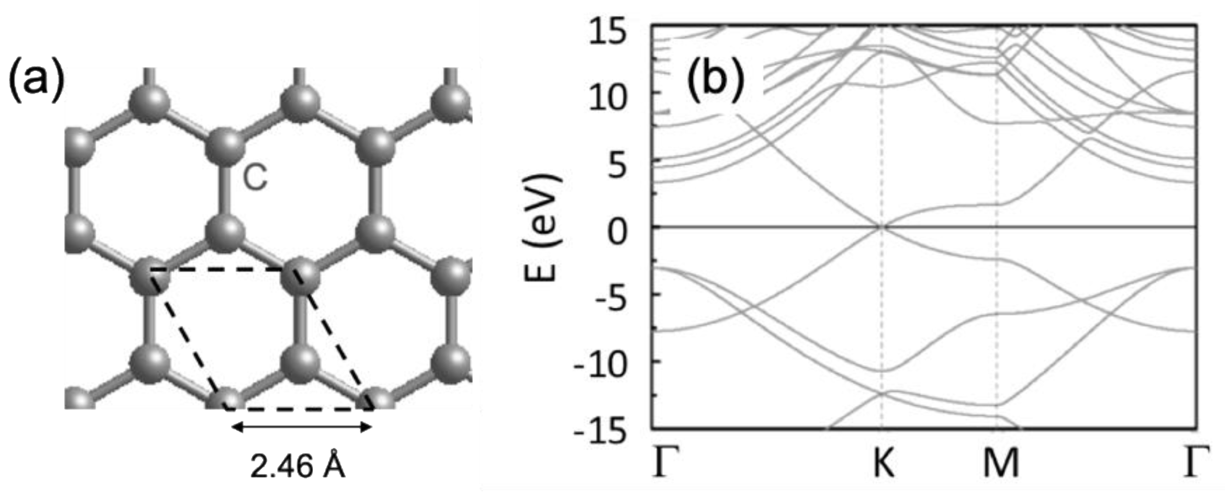
3. Structural and Electronic Properties of Graphene and MoS2

Before discussing the contact resistance at 2D metal/semiconductor interfaces, we briefly present the structural and electronic properties of graphene and MoS2. Graphene consists of a single (flat) layer of carbon atoms, arranged in a hexagonal network, as shown in Figure 3a [41,42,43,44]. The C atoms are sp2-hybridized in graphene, forming two single bonds (σ) and one double bond (σ and π) with their first neighbors. The computed lattice parameter of graphene, using DFT-GGA simulations, is about 2.47 Å [3], typically 0.4% larger than the experimental one, i.e., 2.46 Å [43,44].
The computed electronic band structure of graphene is shown in Figure 3b. The characteristic linear energy dispersion near the Fermi level is clearly observed, forming a so-called Dirac cone; the valence band (corresponding to π orbitals) and the conduction band (corresponding to π * orbitals) touch at the Fermi level EF, resulting in a zero density of states at EF. For this reason, graphene is often called a zero density-of-states metal or a zero band-gap semiconductor. Due to the linear energy band dispersion near the Fermi level, the electrons in graphene are considered as “massless relativistic particles”. This peculiar property results in very high charge carrier mobilities in graphene, in the range of 104–106 cm2/Vs [45,46,47].
MoS2 is a member of the transition metal dichalcogenide family. Monolayer and few-layer MoS2 were investigated recently for their potential use in 2D material-based field-effect transistors and photonic devices [48,49,50,51]. Each molybdenum atom is bonded to six sulfur atoms in MoS2, with three S atoms above and three below, in a trigonal prismatic or octahedral structure, forming a three-layered atomic sheet [52] (see Figure 4a). In bulk MoS2, these sheets are “bonded” via weak Van der Waals forces. In its most stable form, bulk MoS2 crystallizes in the 2H (trigonal prismatic) phase, with a lattice parameter of 3.16 Å; the computed lattice parameter, using DFT-GGA simulations, is about 3.17 Å [3]. Bulk 2H-MoS2 is an indirect semiconductor, with an energy band-gap of about 1.2 eV. The band-gap of MoS2 increases when the number of layers decreases, becoming a direct band-gap semiconductor at the limit of a MoS2 single layer [53,54], with a computed DFT-GGA band-gap of about 1.8 eV [3], as shown in Figure 4b. Depending on the growth conditions and/or on the chemical treatment [17,55], 2H-MoS2 can be transformed to the meta-stable 1T-MoS2 phase. This octahedral phase has a computed lattice parameter of 3.15 Å, and it is metallic [3,56,57,58], as shown in Figure 4c.

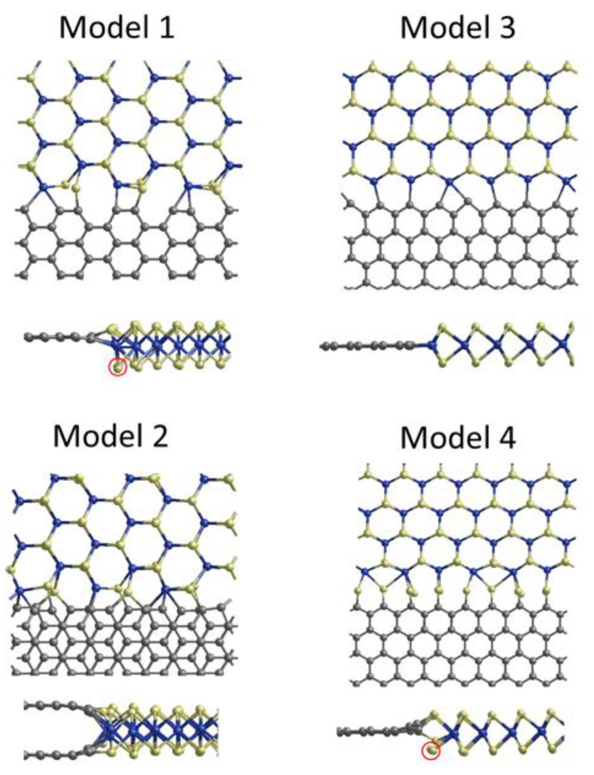
4. Graphene/2H-MoS2 Edge Contacts

We considered four different graphene/monolayer 2H-MoS2 slab models, with various edge contact symmetries and/or terminations, as shown in Figure 5 [59]. Large supercells (with about 250 atoms) were used for the DFT simulations, to minimize the strain in the graphene and MoS2 layers (which is typically below 1.5% in both materials). The zigzag and armchair interface models were built by using (36.5 × 19.4) Å2 and (36.8 × 16.8) Å2 rectangular supercells, respectively. A vacuum layer of about 20 Å was considered for each interface models, to avoid spurious interactions between adjacent cells. Model 1 was based on an armchair–edge interface, with a single graphene layer. After relaxation, carbon–sulfur (2.14 Å average bond length) and carbon–molybdenum (1.83 Å average bond length) bonds were present at this interface, as well as sulfur dangling bonds (from the bottom sulfur sublayer). A graphene bilayer was considered in model 2, in order to saturate these dangling bonds by the formation of C–S bonds. Model 3 was based on a zigzag–edge interface, terminated by Mo atoms, where C–Mo bonds (2.13 Å average bond length) were only present after relaxation, resulting in a “defect-free” contact model. A sulfur-terminated zigzag edge contact was considered in Model 4. In this case, only C–S bonds (1.79 Å average bond length) were formed, but S dangling bonds were present in the bottom sulfur sublayer.
The formation energy γ of the graphene/MoS2 interface is calculated using the following equation [24,60]:
γ = 1 2 L ( E total n C μ C n MO μ MoS 2 Δ n S μ S ) ,
where L is the interface length, Etotal is the total energy of the graphene/MoS2/graphene system, ni and μi are the number of atoms and their chemical potentials, respectively, μMoS2 is the total energy of a MoS2 (single layer) unit cell, and ΔnS = nS − 2nMo. The chemical potential μMo was fixed to that of body-centered cubic Mo, while μS = ½ (μMoS2 − μMo) in the Mo-rich limit, and μS = μS(bulk) in the S-rich limit, where μS(bulk) corresponds to the sulfur chemical potential of a S8 ring [24].
The computed interface formation energies of the slab models are shown in Table 1. The Mo-terminated zigzag interface model (model 3 in Figure 5) was the most stable one, in the molybdenum-rich limit. On the other hand, the armchair interface model, with a bilayer graphene layer, had the lowest γ in the sulfur-rich limit. Note that the Mo and S-terminated zigzag edge contacts, with a graphene monolayer (model 3 and 4), also had comparable interface formation energies in the S-rich limit, with both interfaces likely produced during such a growth process.
The computed RcW of the different edge-contact models is also shown in Table 1. The contact resistances for the “defect-free” interfaces (model 2 and 3) were typically between 220 and 560 Ω.μm. These values are comparable to those reported at graphene/metal edge contacts [61]. On the other hand, the RcW at interfaces with sulfur dangling bonds was about two orders of magnitude larger.
The transmission probabilities of the Mo and S terminated zigzag interface models are discussed below, in order to gain further insight into these results. The computed (zero-bias) transmission spectrum of the molybdenum-terminated zigzag interface model (model 3) is shown in Figure 6a. The onset of transmission is at about 0.1 eV from the Fermi level, a result which is in agreement with the energy barrier height ΦB of about 0.1 eV, calculated from the electrostatic potential profile of the heterostructure [59], as well as from the graphene and MoS2 contributions to the electronic density of states, shown in Figure 6b. Note that the computed graphene work function and MoS2 electron affinity were about 4.4 eV and 4.2 eV, respectively, resulting in an “ideal” interface barrier of 0.2 eV. The barrier height at the Mo-terminated interface model was reduced by about 0.1 eV from the ideal value, due to the presence of polar C–Mo bonds (electrons transferred from Mo to C atoms), forming a dipole layer at the interface, as illustrated in Figure 7a. These C–Mo bonds significantly contributed to the electronic density of states near the Fermi level, as indicated from the isosurface charge density plot shown in the inset of Figure 6b. The resulting low energy barrier at the Mo-terminated zigzag interface led to a low RcW, in the range of 200 Ω∙μm.
The (zero-bias) transmission probability of the S-terminated zigzag interface model, with a large density of sulfur dangling bonds (model 4), is shown in Figure 8a. The onset of the transmission probability was at about 0.4 eV from the Fermi level at this interface, and the transmission was much reduced, in comparison to the molybdenum-terminated interface model. The energy barrier ΦB, extracted from the electrostatic potential profile [59] and the partial electronic density of states, shown in Figure 8b, was increased by about 0.3 eV at the S-terminated contact, due to the presence of S dangling bonds, which produced gap states at about 0.4–0.5 eV below the MoS2 conduction band. The isosurface charge density (see the inset of Figure 8b) indicates that the sulfur dangling bonds significantly contributed to the electronic DOS near the Fermi level, which was pinned by these gap states, resulting in an interface barrier ΦB of about 0.4 eV, as illustrated in Figure 7b. Consequently, the RcW was increased by about two orders of magnitude at this S-terminated zigzag interface, as compared to the Mo-terminated one.

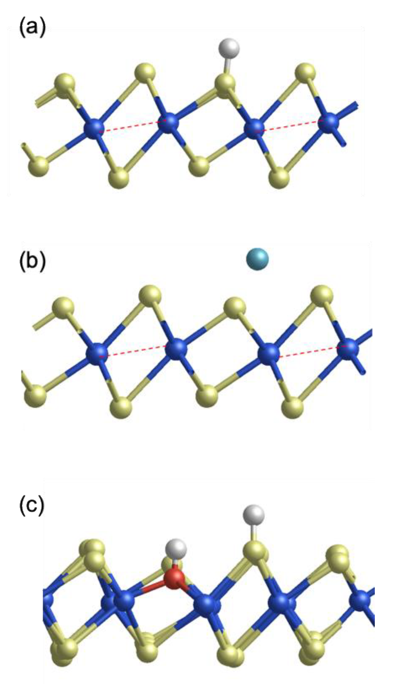
5. T/2H MoS2 Edge Contacts

We considered 1T/2H-MoS2 heterostructures (also based on MoS2 monolayers) with armchair or zigzag edges [62], as shown in Figure 9. The armchair-edge (198 atoms) and zigzag-edge (216 atoms) interface models were obtained by using (35 × 16.5) Å2 and (34 × 19) Å2 rectangular supercells, respectively, with a vacuum layer of 20 Å; the residual strain in the MoS2 layers was typically less than 0.25%.
The relaxed 1T/2H-MoS2 interface models, with armchair and zigzag edges, are shown in Figure 9a,b, respectively. Since the lattice parameters of 1T- and 2H-MoS2 are almost identical, atomically sharp and defect-free interfaces were obtained, in agreement with previous DFT simulations [26].
The computed RcW at the pristine 1T/2H-MoS2 interfaces was about 3–4 × 10⁴ Ω∙μm for the armchair and zigzag edges (see Table 2). The high contact resistance was due to the large interface energy barrier (ΦB ≈ 0.8 eV), which corresponds to the difference between the computed work function of 1T-MoS2m ≈ 5 eV) and the computed electron affinity of 2H-MoS2 (χ 2248 4.2 eV), as schematically illustrated in Figure 10. The calculated interface barrier ΦB ≈ 0.8 eV is in very good agreement (ΦB = 0.82 eV) with other DFT simulations performed on similar 1T/2H-MoS2 heterojunctions [26].
It should be pointed out that the calculated RcW was about two orders of magnitude larger than experimental values reported on 1T-MoS2/2H-MoS2 edge contacts [16,20]. The discrepancy may be explained by assuming that 1T-MoS2 has a lower effective work function, which could arise from its interaction with chemical species during the local semiconducting (2H) to metallic (1T) MoS2 transformation. During device processing, 2H-MoS2 is indeed exposed to n-butyllithium solutions, to induce its transformation to the 1T metallic phase [16,20,63]. During this chemical treatment, chemical species like H, Li, and/or H2O could be adsorbed onto the 1T-MoS2 surface. We, thus, investigated the effect of these adsorbates on the 1T-MoS2 work function. An H atom was adsorbed onto 1T-MoS2 by forming an S–H bond, with a bond length of 1.37 Å (see Figure 11a). On the other hand, Li was most favorably adsorbed onto of an Mo atom, with average Li–Mo distance of 3.07 Å, as indicated in Figure 11b, as in 2H-MoS2 [64]. Interestingly, the formation of the more stable distorted 1T’-phase of MoS2 [56] was promoted by the adsorption of H and Li, as indicated by the distorted Mo atoms forming “one-dimensional (1D) zigzag chains”, which are connected by red dashed lines in Figure 11a,b. We also studied the interaction between a sulfur vacancy and an H2O molecule. An O–H group tended to fill the vacant site, with the O atom bonding to neighbor Mo atoms (2.22 Å average Mo–O bond length); this resulted in the local distortion of the 1T-MoS2 lattice, as indicated in Figure 11c. A neighbor S–H bond was also formed, with a bond length of 1.38 Å.
The adsorption energies Eads of these atoms or molecules on 1T-MoS2 are computed using the following equation:
E a d s = E t o t ( M o S 2 + a d s o r b a t e ) E t o t ( M o S 2 ) E t o t ( a d s o r b a t e ) ,
where the last term, representing the total energy of the adsorbate, was fixed to ½Etot(H2) for H, ½Etot(bulk-Li) for Li, and Etot(H2O) for H2O [62].
All the calculated adsorption energies were negative (see Table 2), indicating that these atoms/molecules were favorably adsorbed onto 1T-MoS2. A partial electron transfer, from the adsorbate to 1T-MoS2, also occurred, which led to its “n-type doping”. Consequently, the adsorption of all these chemical species led to the reduction of the 1T-MoS2 work function; an almost linear decrease of Φm was indeed computed for all the adsorbates considered here [62]. In fact, as shown in Figure 12, the work function shift ΔΦm depended almost linearly on the partial charge transferred between the adsorbate and 1T-MoS2.
The impact of these adsorbates on the contact resistance of 1T/2H-MoS2 heterojunctions is highlighted in Table 2. The adsorbate coverages were fixed to 8% Li, 12% H2O, and 22% H; such coverages are consistent with experimental values obtained during the functionalization of transition-metal dichalcogenide monolayers [65]. The corresponding 1T-MoS2 work function was about 4.3 eV, resulting in an energy barrier at the 1T/2H-MoS2 interface of about 0.1 eV. The functionalization of 1T-MoS2 by the adsorbates subsequently resulted in the decrease of the contact resistance by more than two orders of magnitude (see Table 2), being comparable to the experimental values (100–200 Ω∙μm) reported in References [16] and [20].

6. Concluding Remarks

The potential integration of 2D materials in nanoscale field-effect transistors will require the formation of metal/2D semiconductor contacts with contact resistances in the range of few hundreds of Ω∙μm. First-principles simulations predict that the contact resistance of graphene/monolayer 2H-MoS2 lateral heterostructures strongly depends on the edge contact symmetry and termination. A low contact resistance, in the range of 200 Ω∙μm, was computed at Mo-terminated zigzag edges, due to the possible formation of a “defect-free” interface with a low electron energy barrier. However, the presence of a large density of sulfur dangling bonds at S-terminated (zigzag or armchair) edge contacts resulted in a larger electron energy barrier, with the contact resistance being increased by two orders of magnitude. Obtaining a low contact resistance at graphene/MoS2 lateral heterostructures will, thus, critically depend on the control of the edge symmetry and/or termination.
Another promising 2D metal/2D semiconductor edge contact consists of 1T/2H-MoS2 lateral heterostructures. Low contact resistances, in the range of 200 Ω∙μm, were also predicted from first-principles simulations at such interfaces based on MoS2 monolayers, resulting from the functionalization (electron doping) of the 1T-MoS2 contact by various adsorbates (H, Li, H2O), likely present during the transformation of the stable 2H-MoS2 phase into the meta-stable 1T-MoS2 polymorph. These simulations importantly highlight the beneficial effect of the functionalization of metallic 1T-MoS2 in order to achieve low contact resistances in MoS2-based nanoscale devices.

Author Contributions

DFT simulations, M.H. and R.M.; supervision and project administration, M.H., V.A., and A.S.; writing—review and editing, M.H., V.A., and A.S. All authors have read and agreed to the published version of the manuscript.

Funding

Part of this work was financially supported by the KU Leuven Research Funds (project C14/17/080), and by the European project “2DFun”, an ERA-NET project in the framework of the Graphene Flagship.

Acknowledgments

Fruitful discussions with G. Pourtois, M. Heyns, M. Caymax, and D. Lin (imec) are gratefully acknowledged.

Conflicts of Interest

The authors declare no conflicts of interest.

References

  1. Butler, S.Z.; Hollen, S.M.; Cao, L.Y.; Cui, Y.; Gupta, J.A.; Gutiérrez, H.R.; Heinz, T.F.; Hong, S.S.; Huang, J.X.; Ismach, A.F.; et al. Progress, Challenges, and Opportunities in Two-Dimensional Materials Beyond Graphene. ACS Nano 2013, 7, 2898–2926. [Google Scholar] [CrossRef] [PubMed]
  2. Fiori, G.; Bonaccorso, F.; Iannaccone, G.; Palacios, T.; Neumaier, D.; Seabaugh, A.; Banerjee, S.K.; Colombo, L. Electronics Based on Two-Dimensional Materials. Nat. Nanotechnol. 2014, 9, 768–779. [Google Scholar] [CrossRef] [PubMed]
  3. Miro, P.; Audiffred, M.; Heine, T. An Atlas of Two-Dimensional Materials. Chem. Soc. Rev. 2014, 43, 6537–6554. [Google Scholar] [CrossRef] [PubMed]
  4. Schwierz, F.; Pezoldt, J.; Granzner, R. Two-Dimensional Materials and their Prospects in Transistor Electronics. Nanoscale 2015, 7, 8261–8283. [Google Scholar] [CrossRef] [PubMed] [Green Version]
  5. Molle, A.; Goldberger, J.; Houssa, M.; Xu, Y.; Zhang, S.C.; Akinwande, D. Buckled Two-Dimensional Xene Sheets. Nat. Mater. 2017, 16, 163–169. [Google Scholar] [CrossRef] [PubMed]
  6. Li, X.; Tao, L.; Chen, Z.; Fang, H.; Li, X.; Wang, X.; Xu, J.B.; Zhu, H. Graphene and Related Two-dimensional Materials: Structure-Property Relationships for Electronics and Optoelectronics. Appl. Phys. Rev. 2017, 4, 021306. [Google Scholar] [CrossRef]
  7. Robinson, J.A. 2D for Beyond CMOS. APL Mater. 2018, 6, 058202. [Google Scholar] [CrossRef] [Green Version]
  8. Geim, A.K.; Grigorieva, I.V. Van der Waals Heterostructure. Nature 2013, 499, 419–425. [Google Scholar] [CrossRef]
  9. Huang, C.; Wu, S.; Sanchez, A.M.; Peters, J.J.P.; Beanland, R.; Ross, J.S.; Rivera, P.; Yao, W.; Cobden, D.H.; Xu, X. Lateral Heterojunctions with Monolayer MoSe2-WSe2 Semiconductors. Nat. Mater. 2014, 13, 1096–1101. [Google Scholar] [CrossRef]
  10. Gong, Y.; Lin, J.; Wang, X.; Shi, G.; Lei, S.; Lin, Z.; Zou, X.; Ye, G.; Vajtai, R.; Yakobson, B.I.; et al. Vertical and In-plane Heterostructures from WS2/MoS2 Monolayers. Nat. Mater. 2014, 13, 1135–1142. [Google Scholar] [CrossRef] [Green Version]
  11. Vu, Q.A.; Lee, J.H.; Nguyen, V.L.; Shin, Y.S.; Lim, S.C.; Lee, K.; Heo, J.; Park, S.; Kim, K.; Lee, Y.H. Tuning Carrier Tunneling in Van der Waals Heterostructures for Ultrahigh Detectivity. Nano Lett. 2017, 17, 453–459. [Google Scholar] [CrossRef] [PubMed]
  12. Zhang, C.; Li, M.Y.; Tersoff, J.; Han, Y.; Su, Y.; Li, L.J.; Muller, D.A.; Shih, C.K. Strain Distributions and their Influence in Electronic Structures of WSe2-MoS2 Laterally Strained Heterojunctions. Nat. Nanotech. 2018, 13, 152–158. [Google Scholar] [CrossRef] [PubMed]
  13. Unuchek, D.; Ciarrocchi, A.; Avsar, A.; Watanabe, K.; Taniguchi, T.; Kis, A. Room-Temperature Electrical Control of Exciton Flux in a Van der Waals Heterostructure. Nature 2018, 560, 340–344. [Google Scholar] [CrossRef] [PubMed]
  14. Allain, A.; Kang, J.; Banerjee, K.; Kis, A. Electrical Contacts to Two-Dimensional Semiconductors. Nat. Mater. 2015, 14, 1195–1205. [Google Scholar] [CrossRef] [PubMed]
  15. Schulman, D.S.; Arnold, A.J.; Das, S. Contact Engineering for 2D Materials and Devices. Chem. Soc. Rev. 2018, 47, 3037–3058. [Google Scholar] [CrossRef]
  16. Kappera, R.; Voiry, D.; Yalcin, S.E.; Branch, B.; Gupta, G.; Mohite, A.D.; Chhowalla, M. Phase-Engineered Low-Resistance Contacts for Ultrathin MoS2 Transistors. Nat. Mater. 2014, 13, 1128–1134. [Google Scholar] [CrossRef]
  17. Lin, Y.C.; Dumcenco, D.O.; Hung, Y.S.; Suenaga, K. Atomic Mechanism of the Semiconducting-to-Metallic Phase Transition in Single Layered MoS2. Nat. Nanotech. 2014, 9, 391–396. [Google Scholar] [CrossRef]
  18. Meng, J.; Song, H.D.; Li, C.Z.; Jin, Y.; Tang, L.; Liu, D.; Liao, Z.M.; Xiu, F.; Yu, D.P. Lateral Graphene P-N Junctions Formed by the Graphene/MoS2 Hybrid Interface. Nanoscale 2015, 7, 11611–11619. [Google Scholar] [CrossRef]
  19. Guimaraes, M.H.D.; Gao, H.; Han, Y.; Kang, K.; Xie, S.; Kim, C.J.; Muller, D.A.; Ralph, D.C.; Park, J. Atomically Thin Ohmic Edge Contacts Between Two-Dimensional Materials. ACS Nano 2016, 10, 6392–6399. [Google Scholar] [CrossRef] [Green Version]
  20. Nourbakhsh, A.; Zubair, A.; Sajjad, R.N.; Tavakkoli, A.; Chen, W.; Fang, S.; Ling, X.; Kong, J.; Dresselhaus, M.S.; Kaxiras, E.; et al. MoS2 Field-Effect Transistor with Sub-10 nm Channel Length. Nano Lett. 2016, 16, 7798–7806. [Google Scholar] [CrossRef]
  21. Zhao, M.; Ye, Y.; Han, Y.; Xia, Y.; Zhu, H.; Wang, S.; Wang, Y.; Muller, D.A.; Zhang, X. Large-Scale Chemical Assembly of Atomically Thin Transistors and Circuits. Nat. Nanotech. 2016, 11, 954–959. [Google Scholar] [CrossRef] [PubMed]
  22. Saha, D.; Mahapatra, S. Atomistic Modeling of The Metallic-To-Semiconducting Phase Boundaries in Monolayer MoS2. Appl. Phys. Lett. 2016, 108, 25316. [Google Scholar] [CrossRef] [Green Version]
  23. Saha, D.; Mahapatra, S. Asymmetric Junctions in Metallic-Semiconducting-Metallic Heterophase MoS2. IEEE Trans. Electron Dev. 2017, 64, 2457–2460. [Google Scholar] [CrossRef]
  24. Chen, W.; Yang, Y.; Zhang, Z.; Kaxiras, E. Properties of In-Plane Graphene/MoS2 Heterojunctions. 2D Mater. 2017, 4, 045001. [Google Scholar] [CrossRef]
  25. Liu, X.; Gao, J.; Zhang, G.; Zhang, Y.W. MoS2-Graphene In-Plane Contact for High Interfacial Thermal Conduction. Nano Res. 2017, 10, 2944–2953. [Google Scholar] [CrossRef] [Green Version]
  26. Fan, Z.Q.; Jiang, X.W.; Luo, J.W.; Jiao, L.Y.; Huang, R.; Li, S.S.; Wang, L.W. In-Plane Schottky-Barrier Field-Effect Transistors Based on 1T/2H Heterojunctions of Transition Metal Dichalcogenides. Phys. Rev. B 2017, 96, 165402. [Google Scholar] [CrossRef] [Green Version]
  27. Bai, H.F.; Xu, L.C.; Di, M.Y.; Hao, L.Y.; Yang, Z.; Liu, R.P.; Li, X.Y. The Intrinsic Interface Properties of the Top and Edge 1T/2H MoS2 Contact: A First-Principles Study. J. Appl. Phys. 2018, 123, 095301. [Google Scholar] [CrossRef]
  28. Soler, J.M.; Artacho, E.; Gale, J.D.; Garcia, A.; Junquera, J.; Ordejon, P.; Sanchez-Portal, D. The Siesta Method for Ab-Initio Order-N Materials Simulations. J. Phys. Condens. Matter 2002, 14, 2745–2779. [Google Scholar] [CrossRef] [Green Version]
  29. Perdew, J.P.; Burke, K.; Ernzerhof, M. Generalized Gradient Approximation Made Simple. Phys. Rev. Lett. 1996, 77, 3865–3868. [Google Scholar] [CrossRef] [Green Version]
  30. Trouiller, N.; Martins, J.L. Efficient Pseudopotentials for Plane-Wave Calculations. Phys. Rev. B 1991, 43, 1993–2006. [Google Scholar] [CrossRef]
  31. Bengtsson, L. Dipole Correction for Surface Supercell Calculations. Phys. Rev. B 1999, 59, 12301–12304. [Google Scholar] [CrossRef]
  32. Grimme, S. Semiempirical, GGA-Type Density Functional Constructed with Long-Range Dispersion Correction. J. Comput. Chem. 2006, 27, 1787–1799. [Google Scholar] [CrossRef]
  33. Brandbyge, M.; Mozos, J.L.; Ordejon, P.; Taylor, J.; Stokbro, K. Density-Functional Method for Nonequilibrium Electron Transport. Phys. Rev. B 2002, 65, 165401. [Google Scholar] [CrossRef] [Green Version]
  34. Topsakal, M.; Bagci, V.M.K.; Ciraci, S. Current-Voltage (I-V) Characteristics of Armchair Graphene Nanoribbons Under Uniaxial Strain. Phys. Rev. B 2010, 81, 205437. [Google Scholar] [CrossRef] [Green Version]
  35. Van den Broek, B.; Houssa, M.; Iordanidou, K.; Pourtois, G.; Afanas’ev, V.V.; Stesmans, A. Functional silicene and stanene nanoribbons compared to graphene: Electronic structure and transport. 2D Mater. 2016, 3, 015001. [Google Scholar] [CrossRef]
  36. Iordanidou, K.; Houssa, M.; van den Broek, B.; Pourtois, G.; Afanas’ev, V.V.; Stesmans, A. Impact of point defects on the electronic and transport properties of silicene nanoribbons. J. Phys. Condens. Matter 2016, 28, 035302. [Google Scholar] [CrossRef] [PubMed]
  37. Büttiker, M.; Imry, Y.; Landauer, R.; Pinhas, S. Generalized Many-Channel Conductance Formula with Application to Small Rings. Phys. Rev. B 1985, 31, 6207–6215. [Google Scholar] [CrossRef] [Green Version]
  38. Datta, S. Electronic Transport in Mesoscopic Systems; Cambridge University Press: Cambridge, UK, 1995. [Google Scholar]
  39. Markussen, T.; Rurali, R.; Jauho, A.P.; Brandbyge, M. Scaling Theory Put Into Practice: First-Principles Modeling of Transport in Doped Silicon Nanowires. Phys. Rev. Lett. 2007, 99, 076803. [Google Scholar] [CrossRef] [Green Version]
  40. Datta, S. Lessons From Nanoelectronics: A New Perspective on Transport; World Scientific: Singapore, 2012. [Google Scholar]
  41. Novoselov, K.S.; Geim, A.K.; Morozov, S.V.; Jiang, D.; Zhang, Y.; Dubonos, S.V.; Grigorieva, I.V.; Firsov, A.A. Electric Field Effect in Atomically Thin Carbon Films. Science 2004, 306, 666–669. [Google Scholar] [CrossRef] [Green Version]
  42. Geim, A.K.; Novoselov, K.S. The Rise of Graphene. Nat. Mater. 2007, 6, 183–191. [Google Scholar] [CrossRef]
  43. Katsnelson, M.I. Graphene—Carbon in Two Dimensions; Cambridge University Press: Cambridge, UK, 2012. [Google Scholar]
  44. Foa Torres, L.E.; Roche, S.; Charlier, J.C. Introduction to Graphene-Based Nanomaterials; Cambridge University Press: Cambridge, UK, 2014. [Google Scholar]
  45. Chen, J.H.; Jang, C.; Xiao, S.D.; Ishigami, M.; Fuhrer, M.S. Intrinsic and Extrinsic Performance Limits of Graphene Devices on SiO2. Nat. Nanotech. 2008, 3, 206–209. [Google Scholar] [CrossRef] [PubMed]
  46. Mayorov, A.S.; Gorbachev, R.V.; Morozov, S.V.; Britnell, L.; Jalil, R.; Ponomarenko, L.A.; Blake, P.; Novoselov, K.S.; Watanabe, K.; Taniguchi, T.; et al. Micrometer Scale Ballistic Transport in Encapsulated Graphene at Room Temperature. Nano Lett. 2011, 11, 2396–2399. [Google Scholar] [CrossRef] [PubMed] [Green Version]
  47. Baringhaus, J.; Ruan, M.; Edler, F.; Tejeda, A.; Sicot, M.; Taleb-Ibrahimi, A.; Li, A.P.; Jiang, Z.; Conrad, E.H.; Berger, C.; et al. Exceptional Ballistic Transport in Epitaxial Graphene Nanoribbons. Nature 2014, 506, 349–354. [Google Scholar] [CrossRef] [PubMed]
  48. Radisavljevic, B.; Radenovic, A.; Brivio, J.; Giacometti, V.; Kis, A. Single Layer MoS2 Transistors. Nat. Nanotech. 2011, 6, 147–150. [Google Scholar] [CrossRef] [PubMed]
  49. Radisavljevic, B.; Whitwick, M.B.; Kis, A. Integrated Circuits and Logic Operations Based on Single-Layer MoS2. ACS Nano 2011, 5, 9934–9938. [Google Scholar] [CrossRef]
  50. Lopez-Sanchez, O.; Lembke, D.; Kayci, M.; Radenovic, A.; Kis, A. Ultrasensitive Photodectors based on Monolayer MoS2. Nat. Nanotech. 2013, 8, 497–501. [Google Scholar] [CrossRef]
  51. Molina-Mendoza, A.J.; Vaquero-Garzon, L.; Leret, S.; de Juan-Fernandez, L.; Perez, E.M.; Castellanos-Gomez, A. Engineering the Optoelectronic Properties of MoS2 Photodetectors through reversible noncovalent functionalization. Chem. Commun. 2016, 52, 14365. [Google Scholar] [CrossRef] [Green Version]
  52. Kuc, A. Low-Dimensional Transition Metal Dichalcogenides. Chem. Modelling 2014, 11, 1–29. [Google Scholar]
  53. Mak, K.F.; Lee, C.; Hone, J.; Shan, J.; Heinz, T.F. Atomically Thin MoS2: A New Direct Gap Semiconductor. Phys. Rev. Lett. 2010, 105, 136805. [Google Scholar] [CrossRef] [Green Version]
  54. Scalise, E.; Houssa, M.; Pourtois, G.; Afanas’ev, V.V.; Stesmans, A. Strain-Induced Semiconductor to Metal Transition in the Two-Dimensional Honeycomb Structure of MoS2. Nano Res. 2012, 5, 43–48. [Google Scholar] [CrossRef]
  55. Voiry, D.; Mohite, A.; Chhowalla, M. Phase Engineering of Transition Metal Dichalcogenides. Chem. Soc. Rev. 2015, 44, 2702–2712. [Google Scholar] [CrossRef] [PubMed]
  56. Enyashin, A.; Yadgarov, L.; Houben, L.; Popov, I.; Weidenbach, M.; Tenne, R.; Bar-Sadan, M.; Seifert, G. New Route for Stabilization of 1T-WS2 and MoS2 Phases. J. Phys. Chem. C 2011, 115, 24586–24591. [Google Scholar] [CrossRef] [Green Version]
  57. Qian, X.; Liu, J.; Fu, L.; Li, J. Quantum Spin Hall Effect in Two-Dimensional Transition Metal Dichalcogenides. Science 2014, 346, 1344–1347. [Google Scholar] [CrossRef] [PubMed] [Green Version]
  58. Saha, D.; Mahapatra, S. Anisotropic Transport in 1T’ Monolayer MoS2 and its Metal Interfaces. Phys. Chem. Chem. Phys. 2017, 19, 10453–10461. [Google Scholar] [CrossRef]
  59. Houssa, M.; Iordanidou, K.; Dabral, A.; Lu, A.; Meng, R.; Pourtois, G.; Afanas’ev, V.V.; Stesmans, A. Contact Resistance at Graphene/MoS2 Lateral Heterostructures. Appl. Phys. Lett. 2019, 114, 163101. [Google Scholar] [CrossRef]
  60. Bollinger, M.V.; Jacobsen, K.W.; Nørskov, J.K. Atomic and Electronic Structure of MoS2 Nanoparticles. Phys. Rev. B 2003, 67, 085410. [Google Scholar] [CrossRef] [Green Version]
  61. Song, S.M.; Kim, T.Y.; Sul, O.J.; Shin, W.C.; Cho, B.J. Improvement of Graphene-Metal Contact Resistance by Introducing Edge Contacts at Graphene Under Metal. Appl. Phys. Lett. 2014, 104, 183506. [Google Scholar] [CrossRef]
  62. Houssa, M.; Iordanidou, K.; Dabral, A.; Lu, A.; Pourtois, G.; Afanas’ev, V.V.; Stesmans, A. Contact Resistance at MoS2-Based 2D Metal/Semiconductor Lateral Heterojunctions. ACS Appl. Nano Mater. 2019, 2, 760. [Google Scholar] [CrossRef]
  63. Chou, S.S.; Sai, N.; Lu, P.; Coker, E.N.; Liu, S.; Artyushkova, K.; Luk, T.S.; Kaehr, B.; Brinker, C.J. Understanding Catalysis in a Multiphasic Two-Dimensional Transition Metal Dichalcogenide. Nat. Commun. 2015, 6, 8311. [Google Scholar] [CrossRef]
  64. Dolui, K.; Rungger, I.; Pemmaraju, C.D.; Sanvito, S. Possible Doping Strategies for MoS2 Monolayers: An Ab-Initio Study. Phys. Rev. B 2013, 88, 075420. [Google Scholar] [CrossRef] [Green Version]
  65. Voiry, D.; Goswani, A.; Kappera, R.; de Carvalho Castro e Silva, C.; Kaplan, D.; Fujita, T.; Chen, M.; Asefa, T.; Chhowalla, M. Covalent Functionalization of Monolayered Transition Metal Dichalcogenides by Phase Engineering. Nat. Chem. 2014, 7, 45–49. [Google Scholar] [CrossRef] [PubMed]
Figure 1. Schematic two terminal device used for the non-equilibrium Green’s function (NEGF) transport simulation. The electrochemical potentials of the left (μ1) and right (μ2) electrodes are shifted by qV when a bias V is applied to the structure. The self-energies Γ1 and Γ2 at the contacts are also indicated.
Applsci 10 02731 g001
Figure 2. (a) Computed current–voltage (I–V) characteristics of a 1T-MoS2/2H-MoS2/1T-MoS2 heterostructure. The resistance R of the structure is extracted from a linear fit to the data (solid line), in the voltage range between 0.2 and 0.8 V. (b) Resistance (multiplied by the channel width W) of the same heterostructure, for three different 2H-MoS2 channel lengths. The dashed line is a linear fit to the data.
Applsci 10 02731 g002
Figure 3. (a) Top view of the atomic configuration of graphene. (b) Computed electronic band structure of graphene. The Fermi level corresponds to the reference (zero energy) level.
Applsci 10 02731 g003
Figure 4. (a) Schematic representations of 2H, 3R, and 1T phases of transition metal dichalcogenides. (b) Computed electronic band structure of a 2H-MoS2 monolayer. The reference energy level corresponds to the valence band edge. (c) Computed electronic band structure of a 1T-MoS2 monolayer. The reference energy level corresponds to the Fermi level.
Applsci 10 02731 g004
Figure 5. Top and side views of the relaxed atomic configurations of lateral graphene/MoS2 interface models [59]. Model 1 and model 2 correspond to armchair edge contacts, with a single graphene layer and a double graphene layer, respectively. Models 3 and 4 correspond to zigzag edge contacts with Mo termination and S termination, respectively. Dark-gray, blue, and yellow spheres correspond to C, Mo, and S atoms, respectively. The S dangling bonds in model 1 and model 4 are encircled in red.
Applsci 10 02731 g005
Figure 6. (a) Computed transmission spectrum (at zero bias) of a graphene/MoS2 lateral heterostructure with Mo-terminated zigzag edge contacts (model 3 in Figure 5). The Fermi level corresponds to the reference (zero) energy. (b) Partial electronic density of states (PDOS) of graphene and MoS2. The inset shows the isosurface charge density (0.01 e/Å3) near the Fermi level. Adapted from Reference [59].
Applsci 10 02731 g006
Figure 7. (a) Schematic energy band diagram of (a) Mo-terminated and (b) S-terminated zigzag edge graphene/MoS2 interfaces.
Applsci 10 02731 g007
Figure 8. (a) Computed transmission spectrum (at zero bias) of a graphene/MoS2 lateral heterostructure with S-terminated zigzag edge contacts (model 4 in Figure 5). The Fermi level corresponds to the reference (zero) energy. (b) Partial electronic density of states (PDOS) of graphene and MoS2. The inset shows the isosurface charge density (0.01 e/Å3) near the Fermi level. Adapted from Reference [59].
Applsci 10 02731 g008
Figure 9. Top views of the relaxed atomic configurations of lateral 1T-MoS2/2H-MoS2 interface models with (a) armchair and (b) zigzag edge contacts. Blue and yellow spheres correspond to Mo and S atoms, respectively.
Applsci 10 02731 g009
Figure 10. Schematic energy band diagram of a 1T-MoS2/2H-MoS2 lateral heterojunction [62].
Applsci 10 02731 g010
Figure 11. Side views of the relaxed atomic configurations of 1T-MoS2 surfaces with different adsorbates: (a) H atom, (b) Li atom, and (c) H2O molecule, interacting with a sulfur vacancy [62].
Applsci 10 02731 g011
Figure 12. Computed work function shift ΔΦm as a function of the charge transferred to the 1T-MoS2 layer (calculated as the product of the adsorbate coverage and partial charge transferred to 1T-MoS2 from Table 2) [62]. The dashed line guides the eye.
Applsci 10 02731 g012
Table 1. Computed interface formation energies γ of the different graphene/MoS2 interface models shown in Figure 5, in the Mo-rich and S-rich limit, respectively. The value of the computed contact resistance RcW of each interface model is also given.
Interface Modelγ (eV/Å)
Mo-Rich Limit
γ (eV/Å)
S-Rich Limit
RcW (Ω.μm)
Model 12.42.48.1 × 103
Model 21.51.55.6 × 102
Model 31.21.82.2 × 102
Model 42.61.92.3 × 104
Table 2. Computed contact resistance, adsorption energies Eads and electron transfer (Hirshfeld population analysis) of the different 1T/2H-MoS2 interface models. The adsorption energies and charge transfer were computed for one adsorbed atom or molecule on a (4 × 4) 1T-MoS2 supercell.
Interface ModelRcW (Ω∙μm)Eads (eV)Electron Transfer to 1T-MoS2 (e)
Pristine armchair contact3.8 × 104//
Pristine zigzag contact2.9 × 104//
H-adsorbed contact2.8 × 102−0.750.05
Li-adsorbed contact1.9 × 102−1.460.18
H2O-adsorbed contact4.7 × 102−2.430.08

