Article

Facile Synthesis of Highly Conductive Vanadium-Doped NiO Film for Transparent Conductive Oxide

Multifunctional Hybrid Nanomaterials Laboratory, School of Chemical Engineering, Jeonbuk National University, Jeonju 54896, Korea
*
Author to whom correspondence should be addressed.
Appl. Sci. 2020, 10(16), 5415; https://doi.org/10.3390/app10165415
Submission received: 3 July 2020 / Revised: 21 July 2020 / Accepted: 31 July 2020 / Published: 5 August 2020
(This article belongs to the Special Issue Advances in Future Energy Materials)

Abstract

:
Metal-oxide-based electrodes play a crucial role in various transparent conductive oxide (TCO) applications. Among the p-type materials, nickel oxide is a promising electrically conductive material due to its good stability, large bandgap, and deep valence band. Here, we display pristine and 3 at.%V-doped NiO synthesized by the solvothermal decomposition method. The properties of both the pristine and 3 at.%V:NiO nanoparticles were characterized by field emission scanning electron microscopy (FESEM), transmission electron microscopy (TEM), X-ray diffractometry (XRD), Raman spectroscopy, ultraviolet–visible spectroscopy (UV–vis), and X-ray photoelectron spectroscopy (XPS). The film properties were characterized by atomic force microscopy (AFM) and a source meter. Our results suggest that incorporation of vanadium into the NiO lattice significantly improves both electrical conductivity and hole extraction. Also, 3 at.%V:NiO exhibits a lower crystalline size when compared to pristine nickel oxide, which maintains the reduction of surface roughness. These results indicate that vanadium is an excellent dopant for NiO.

1. Introduction

Nickel oxide (NiO) is one of the rare metal oxide semiconductors, exhibiting a wide bandgap of ~3.6 eV [1,2,3]. It has been used in numerous practical applications, such as organic light-emitting diodes [4], sensors [5], supercapacitors [6], and solar cells [7]. There are many literature reports available on the synthesis of NiO nanoparticles (NPs) [8,9,10,11]. However, there have been difficulties in preparing a well-dispersed ultra-small NiO ink for transparent conductive oxide (TCO) applications [12,13]. In reality, electrode fabrication using pre-annealed NiO nanoparticles is difficult due to their lower dispersibility and poor adhesion on TCO substrates. Capping agents like oleylamine and oleic acid added during the synthesis of the metal oxide are beneficial for the suppression of particle growth and can eventually result in monodispersed metal oxide nanoparticles with great dispersion in DI water.
In recent reports, NiO has been used as a hole transport layer (HTL) in inverted perovskite solar cells [14,15,16] and organic light-emitting diodes (LEDs) [17]. In principle, to enhance the performance of solar cells and OLEDs, one needs to meet the following general requirements: better electrical conductivity, efficient charge transport, solution processing under low temperature, and bandgap tuning [18]. Improved electrical conductivity and hole extraction can be achieved through doping [19]. Different dopants have been used to improve the conductivity of NiO, such as Cs [19], Cu [20], Nb [21], Y [22], Ag [1,2,3,4,5,6,7,8,9,10,11,12,13,14,15,16,17,18,19,20,21,22,23,24], Co [25], N [26], and K [27]. Among all these dopants, Cu is widely used for light doping in various TCO-based applications.
In a study of AgxNixO film, Jun-Dar et al. reported that the Ni+3/Ni+2 ratio was enhanced by varying concentrations of Ag content [23]. They also reported that an increased Ni+3/Ni+2 ratio significantly increased the hole concentration. Another study by Sharma R et al. reported that the hole concentration of NiO is enhanced by light Ag doping, and the product was applied in heterojunction diodes (HJDs) [24].
A notable study by Wei Chen et al. [20] demonstrated that Cu doping on NiO drastically enhances the electrical conductivity of NiO. More recently, Julien et al. reported that N-doped NiO showed improved conductivity as compared to undoped NiO due to the influence of Ni vacancies [26]. The work of Islam et al. also demonstrated NiO film with superior conductivity due to a higher ratio of Ni3+ to Ni2+ [28].
In this work, for the first time (to the best of our knowledge), we studied the optical, morphological, and electrical conductivity properties of V:NiO nanoparticles. Our main aim is to investigate how to modify NiO film conductivity on the TCO substrate. So, we substituted Ni with varying atomic percentages of vanadium in the NiO lattice. A comparative study of pristine NiO and 3 at.%V:NiO showed improvements in film morphology and conductivity for 3 at.%V:NiO as compared to pristine NiO film. Both the pristine and V-doped NiO were prepared by the solvothermal decomposition method. Ultra-small-sized, highly crystalline, pre-annealed nanoparticles were used for deposition on the TCO substrate. However, the effect of vanadium doping on NiO has not been widely studied.

2. Materials and Methods

2.1. Materials and Methods

Materials, including Ni (II) acetylacetonate (C10H14NiO4), oleylamine (C18H37N), borane tri-ethylamine [(C2H5)3NBH3], and vanadium pentoxide (V2O5), were purchased from Sigma-Aldrich.

2.2. Characterization

The properties of both pristine and vanadium-doped NiO (V:NiO) nanoparticles were characterized by field emission scanning electron microscopy (FESEM, Hitachi S-4700, Tokyo, Japan), transmission electron microscopy (TEM, JEM-2010-JEOL, Tokyo, Japan), X-ray diffractometry (XRD, PANalytical X’Pert PRO, Almelo, The Netherlands), Raman spectroscopy (Renishaw, UK), ultraviolet–visible spectroscopy (UV–vis, Jasco V-670, Easton, MD, USA), and X-ray photoelectron spectroscopy (XPS, AXIS-NIVA CJ 109, Kratos, Manchester, UK). The film properties were characterized by tapping-mode atomic force microscopy (Bruker, Multimode-8, Billerica, MA, USA) and a source meter (Keithley-2450, Beaverton, OR, USA).

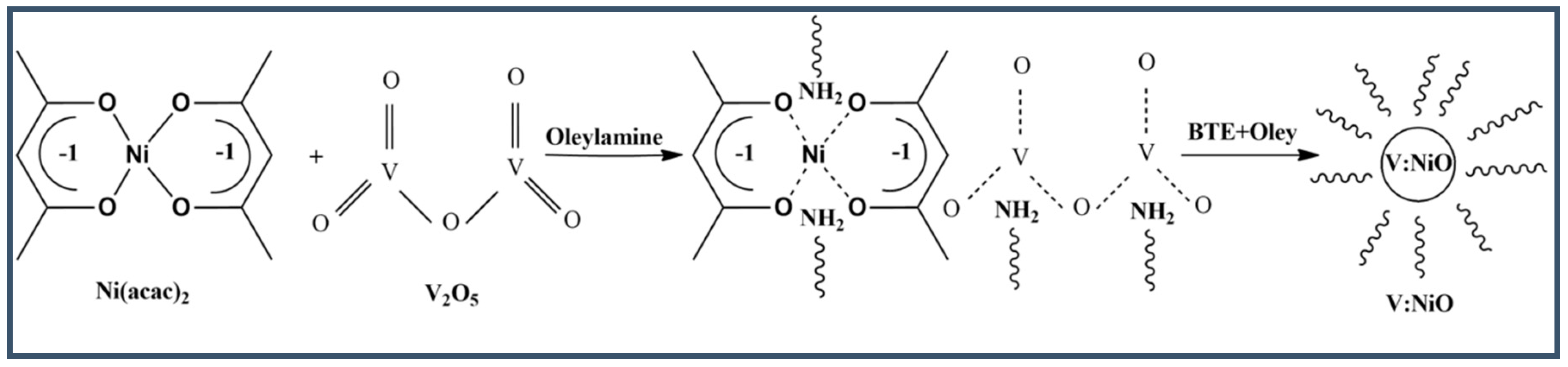
2.3. Synthesis of Pristine and V-Doped NiO

Nickel oxide (NiO) nanoparticles were synthesized by the solvothermal decomposition method. Briefly, 1 mmol of Ni(II) acetylacetonate was dissolved in 15 mL of oleylamine. The solution was kept in a two-necked round flask and heated to 110 °C with continuous stirring under nitrogen flow for 45 min. The obtained clear blue solution was then cooled to and maintained at 90 °C. Next, a mixture of 0.4 mL of borane tri-ethylamine and 2 mL oleylamine was quickly injected into the clear solution. The resulting dark solution was continuously stirred for 1 h. The resultant solution containing ultra-small-sized NiO nanoparticles was collected via 6000 rpm centrifugation for 15 min. Then, the NPs were washed in ethanol three times. To obtain the vanadium-doped NiO (V:NiO), different atomic percentages of vanadium pentoxide were added to the initial Ni(II) acetylacetonate and oleylamine solution. All other conditions were similar to those for the synthesis of the pristine NiO. In this reaction, oleylamine acts as a capping agent, which helps to reduce particle growth, and borane tri-ethylamine was used as a reducing agent, as shown in Scheme 1. As-synthesized pristine NiO and V:NiO were easily dispersed in DI water by 30 min ultra-sonication. Pristine and doped NiO films were deposited under room temperature on cleaned FTO glass substrates by spin coating (2500 rpm, 60 s) with the solutions mentioned above.

3. Results

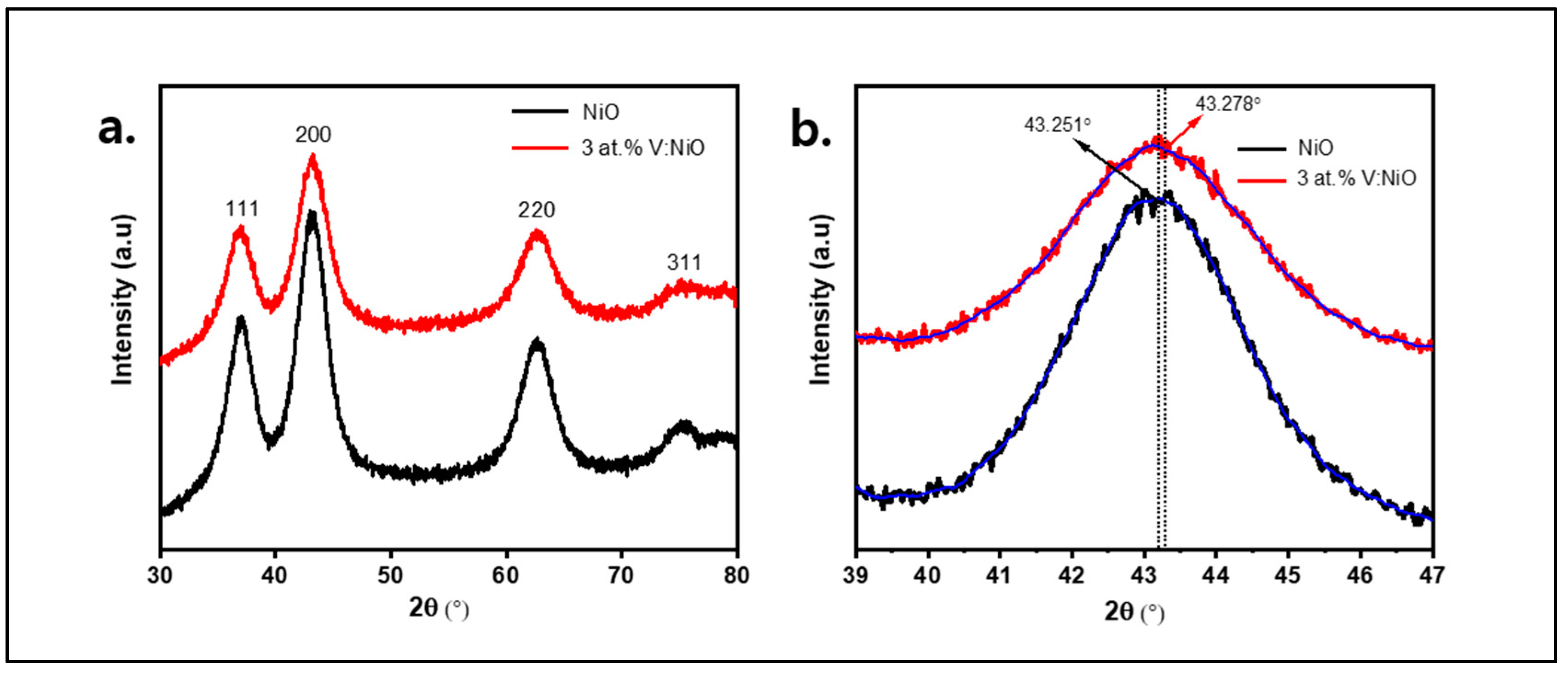
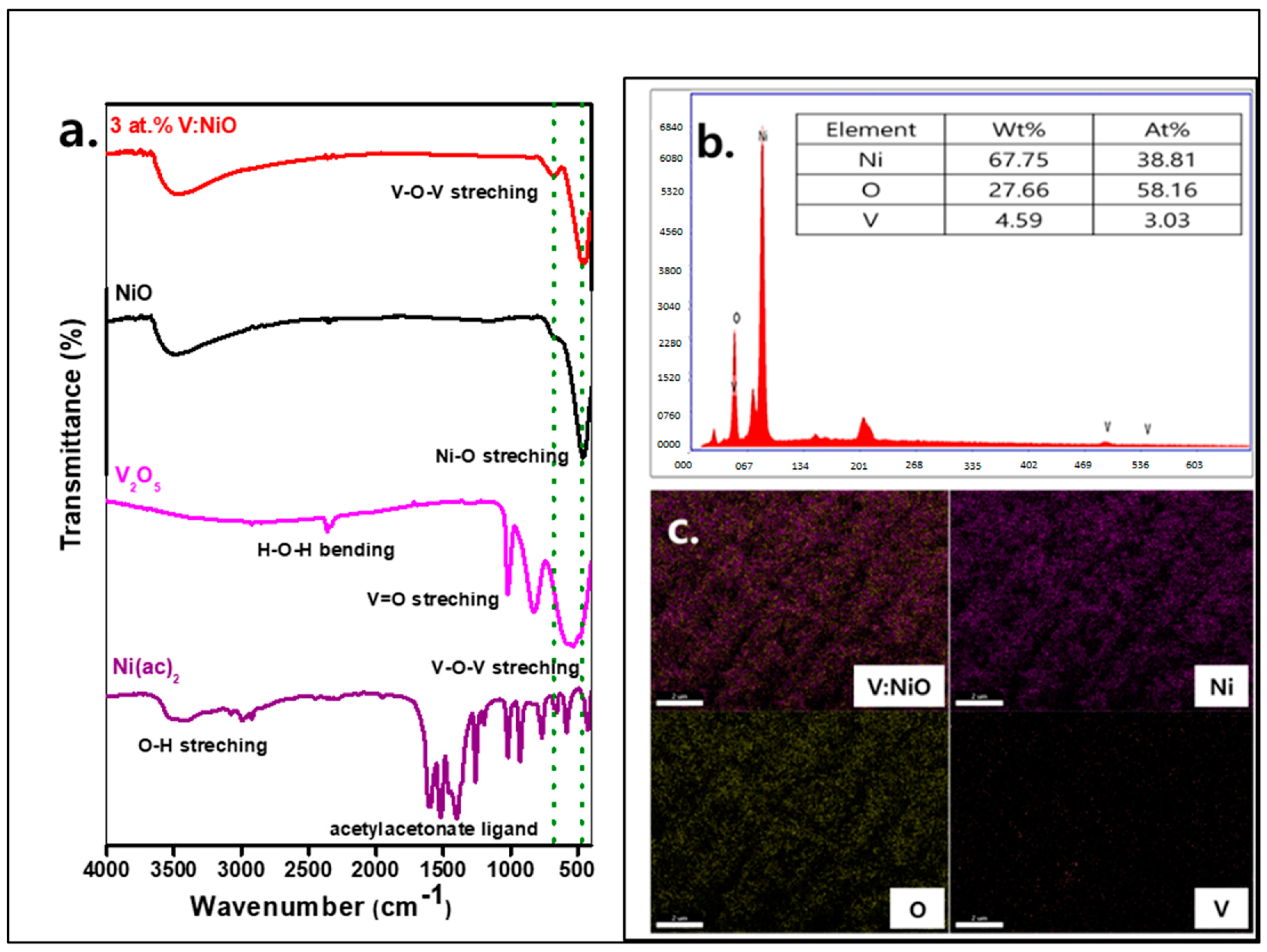
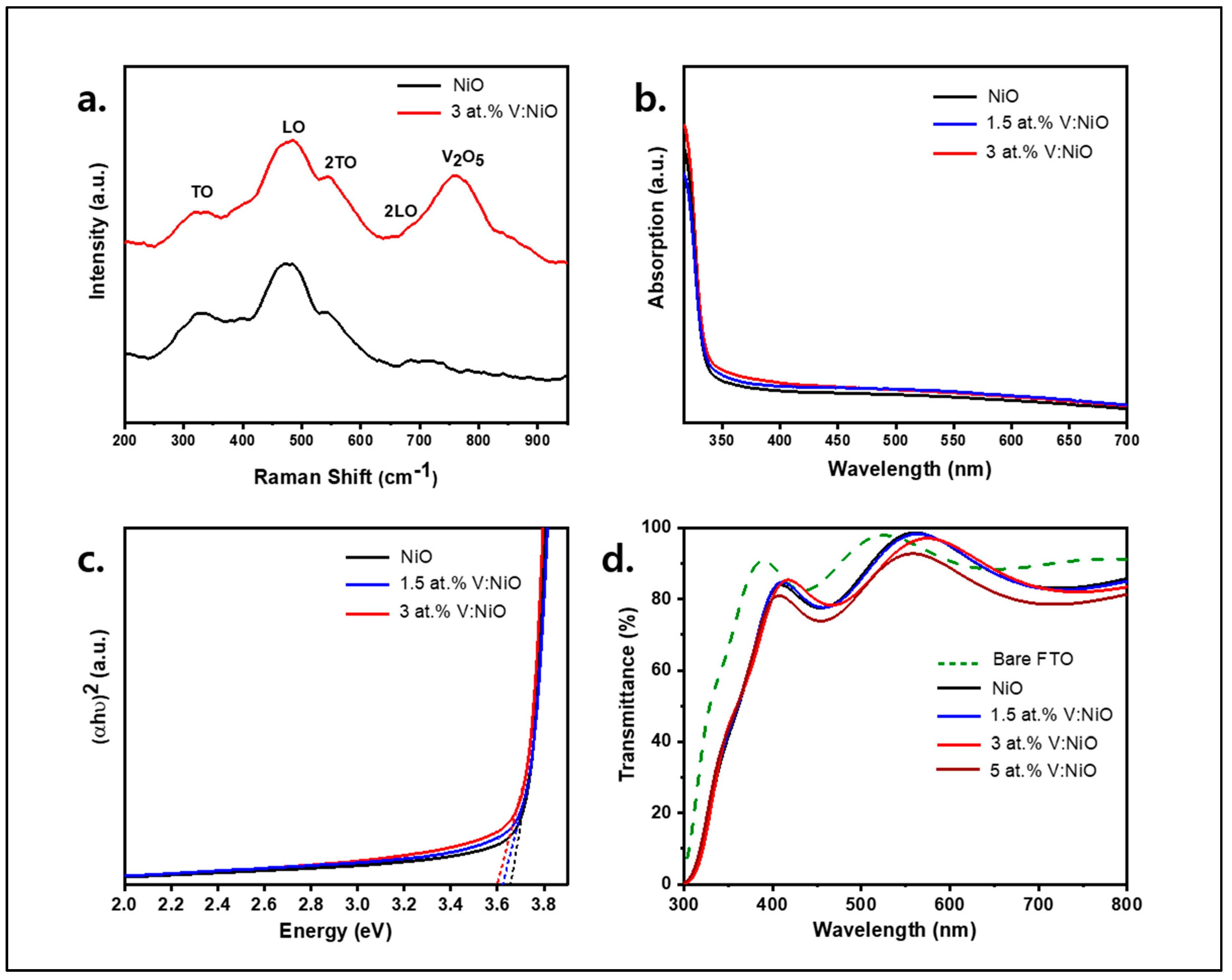
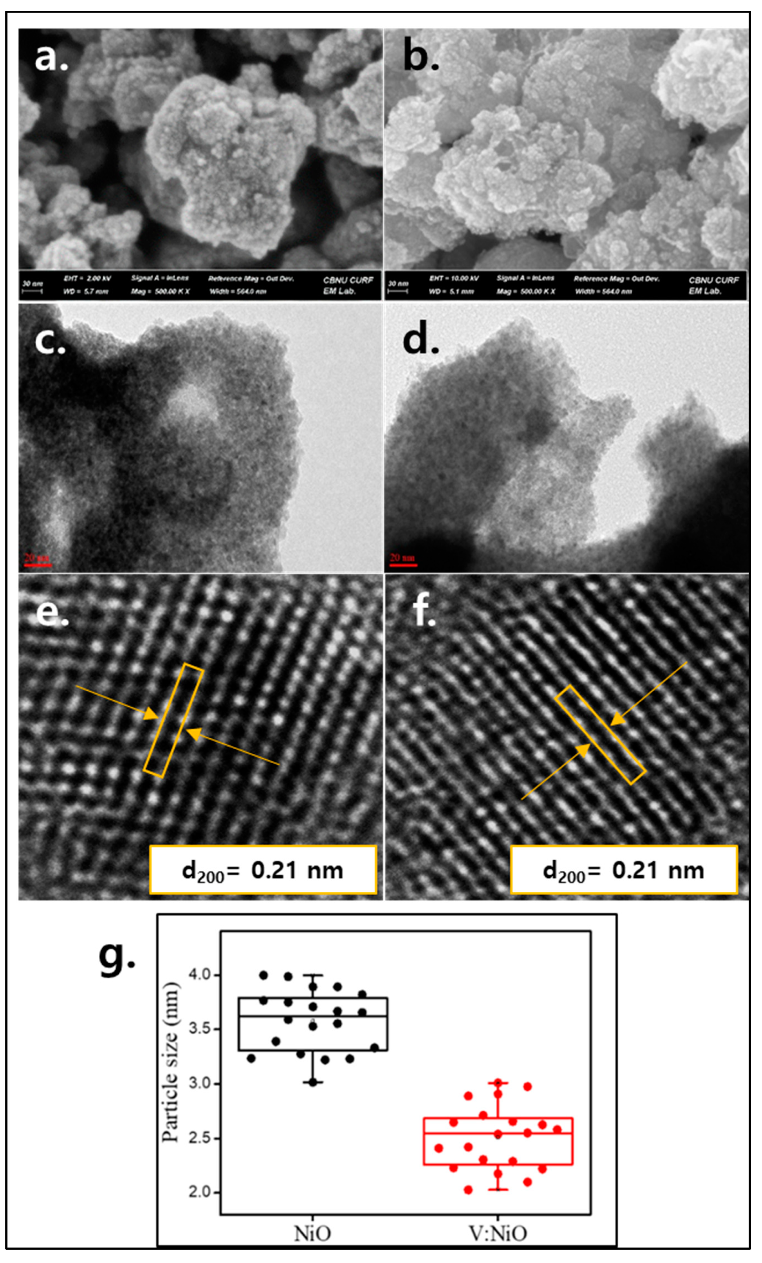
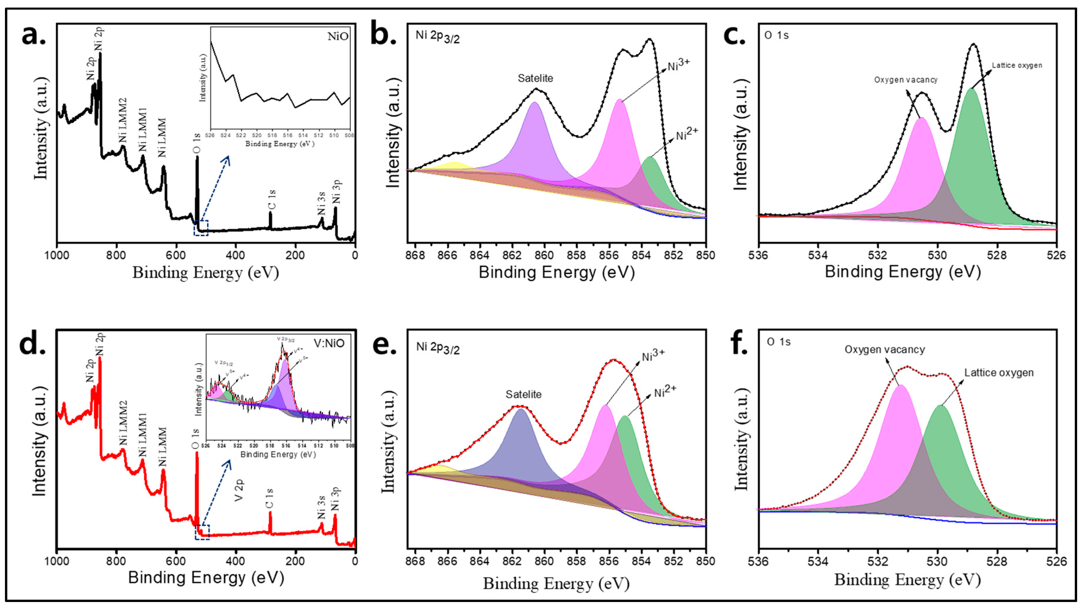
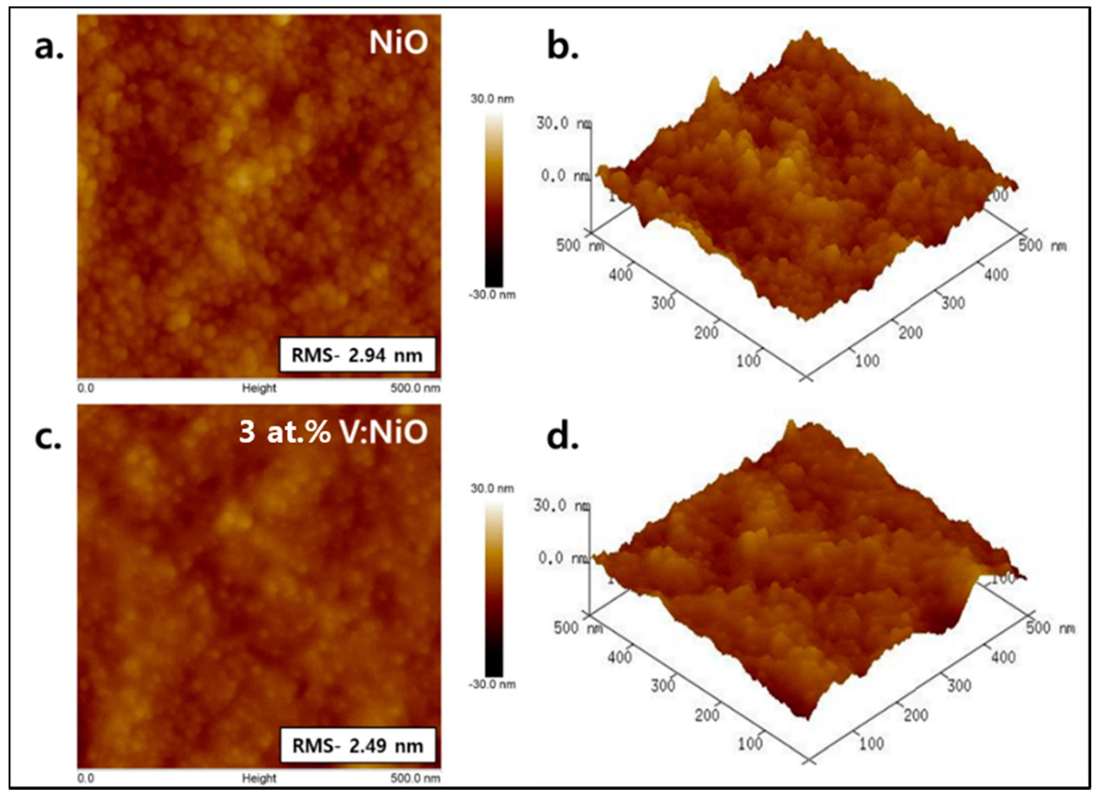
3.1. Study of Material Properties

To study the effect of V doping on NiO, the materials were subjected to analysis using XRD. In our work, both pristine and 3 at.%V:NiO NPs exhibited a very broad XRD pattern (Figure 1a). The diffraction peaks of the prepared powder samples show a cubic face-centered crystal system with four characteristic diffraction peaks at 2θ = 36.98°, 43.21°, 62.67°, and 75.34°, which could be assigned to the (111), (200), (220), and (311) planes of NiO, respectively. The synthesized NiO NP formation was confirmed using the Joint Committee on Powder Diffraction Standards (JCPDS) card no. 03-065-2901 with space group Fm3m [29]. Meanwhile, no extra diffraction peaks related to vanadium or vanadium oxide were observed. A similar trend was also observed for the 1.5 at.%V:NiO sample, but an extra diffraction peak of V2O5 was observed at a higher doping percentage (5 at.%V:NiO). This result indicates that a light doping concentration of V hardly changes the phase structure of NiO [2]. Additionally, it could be observed that the 3 at.%V:NiO NP diffraction peak at 43.251° shows a broadening and slight shifting towards a higher angle (Figure 1b). This result indicates the incorporation of vanadium into the NiO lattice. It is also important to mention that the diffraction peak broadening of the 3 at.%V:NiO sample reveals the reduction of particle size. To further understand the effect of particle size after doping, we calculated the crystalline size of both samples by the Debye–Scherrer formula, D p = 0.89   λ cos , where Dp is the crystalline size, λ is the X-ray wavelength, β is the full width at half-maximum (FWHM), and θ is the diffraction angle of the peak. Interestingly, we observed that the crystalline size of peak (200) significantly decreased after doping from 3.09 nm to 2.82 nm. Hence, the dissociation density (δ) and lattice strain (ε) were calculated by the equations [30] = 1 D p 2   and = cos / 4 , and values are tabulated in Table 1. It can be concluded that the NiO crystalline size was decreased by V doping; thereby, the dissociation density and lattice strain were enhanced.
Figure 2a shows the FTIR spectra of Ni(ac)2, V2O5, NiO, and 3 at.%V:NiO for a comparative study of the precursor materials and products. In our case, the characteristic stretching vibration of the Ni-O absorption band was observed at 468 cm−1, which originated from the Ni(ac)2 species. The peak at 676 cm−1 in the doped sample was ascribed to the presence of vanadium. We observed that the Ni-O stretching band in NiO and the V-O-V stretching band in the 3 at.%V:NiO sample were shifted to lower wavenumber regions as compared with the Ni(ac)2 and V2O5 precursor samples. These red shifts are associated with changes in the surface area and surface defects due to the oleylamine (capping agent) added during the synthesis.
The elemental compositions of both the pristine and 3 at.%V:NiO NPs were confirmed by energy-dispersive X-ray spectroscopy (EDAX). Figure 2b shows that the 3 at.%V:NiO powder sample consisted of Ni, V, and O with no impurity elements. The weight and atomic percentage values of the Ni, O, and V elements are given in the inset of Figure 2b. The EDX mapping of elements in Figure 2c revealed the uniform distribution of Ni, V, and O in the sample.
The Raman spectra of NiO and 3 at.%V:NiO are given in Figure 3a. From the analysis, four characteristic Raman peaks were positioned in both samples, corresponding to the shaking peaks of NiO. The peaks at 324 and 479 cm−1 are the first-order transverse optical (TO) and longitudinal optical (LO) phonon modes of NiO NPs, respectively. The peaks at 546 and 686 cm−1 are because of the combination of 2TO and 2LO. Meanwhile, an extra peak observed at 760 cm−1 can be associated with the V-O stretching mode in the 3 at.%V:NiO sample. This result shows that vanadium can be incorporated with oxygen.
Figure 3b, c depicts the results of ultraviolet–visible spectroscopy studies of ethanol-dispersed pristine and doped NiO samples. A gradual red shift in the absorption spectra with increasing V concentration is observed from Figure 3b. This shift is consistent with the incorporation of V5+ into the NiO lattice. This indicates that the band gap energy in 3 at.%V:NiO is lower than that in pristine NiO. Meanwhile, the optical band gap estimated for pristine NiO NPs by Tauc plot (Figure 3c) was around 3.65 eV, which is well matched with the previously reported values [2,3]. In NiO NPs doped with different percentages of V, it was clear that after introducing vanadium content into the NiO crystal lattice, the optical band gap was slightly reduced to 3.62 eV for 1.5 at.%V:NiO and 3.59 eV for 3 at.%V:NiO.
It is important to study the optical transmission spectra of pristine NiO and V:NiO films, shown in Figure 3d. Both NiO and V:NiO films coated on an FTO substrate still exhibited high transmission (>80%) in the visible region. A small variation in transmission was observed for both 1.5 and 3 at.%V:NiO films when compared to that for the pristine NiO. However, we also noticed that the optical transmittance decreased with increasing V doping percentage. NiO film with a higher doping percentage (5 at.%V:NiO) exhibited low transmission as compared to the pristine NiO film, while V:NiO film with 3 at.% V doping content exhibited transmittance higher than 80% for the visible range. Therefore, the optimized V content of 3 at.% for NiO NPs was used for further studies.
FESEM micrographs with higher-resolution images of pristine NiO and 3 at.%V:NiO powder samples are shown in Figure 4a,b. The samples exhibit similar morphology with ultra-small-sized spherical structures that are agglomerated. TEM images showing the same sample morphology are displayed in Figure 4c,d. The particle diameters are summarized in Figure 4g. The statistical distributions of the nanoparticle diameters of pristine NiO and 3 at.%V:NiO were measured to be ~3.5 ± 0.5 nm and ~2.5 ± 0.5 nm, respectively. This result was consistent with the result of XRD. The particle size variations in the TEM analysis of both samples may be due to the influence of large Ni ions (ionic radius, 0.83 A°) replaced by small V ions (ionic radius, 0.72 A°). Meanwhile, the HRTEM results revealed that the interplanar distance of both samples in Figure 4e,f was 0.21 nm.
Elemental analysis was performed via X-ray photoelectron spectroscopy. The survey spectra of pristine NiO (Figure 5a) confirmed the presence of Ni and O elements, whereas Ni, O, and V elements were confirmed in the 3 at.%V:NiO sample (Figure 5d). Typically, NiO 2P3/2 consists of a main peak at 854 eV, shoulder peak at 856 eV, and shake-up satellite peak at 861 eV [31]. No major changes were observed in a comparison of the Ni 2P3/2 spectra of both pristine and doped samples (Figure 5b,e). However, in the case of the doped sample, we detected the presence of V4+ and V5+ in the binding energy range between 526 eV and 510 eV, which reveals that V atoms were successfully incorporated into the NiO crystal lattice. Interestingly, after V occupied the interstitial sites in the NiO lattice, Ni3+ ions were possibly induced by V5+ ions (Figure 5e). Further, we calculated the Ni3+/Ni2+ ratios to be 0.96 and 1.04 for the NiO and 3 at.%V:NiO samples, respectively. The higher density of Ni3+ states in the 3 at.%V:NiO crystal would contribute to the improvement of p-type conductivity [23,24,31].

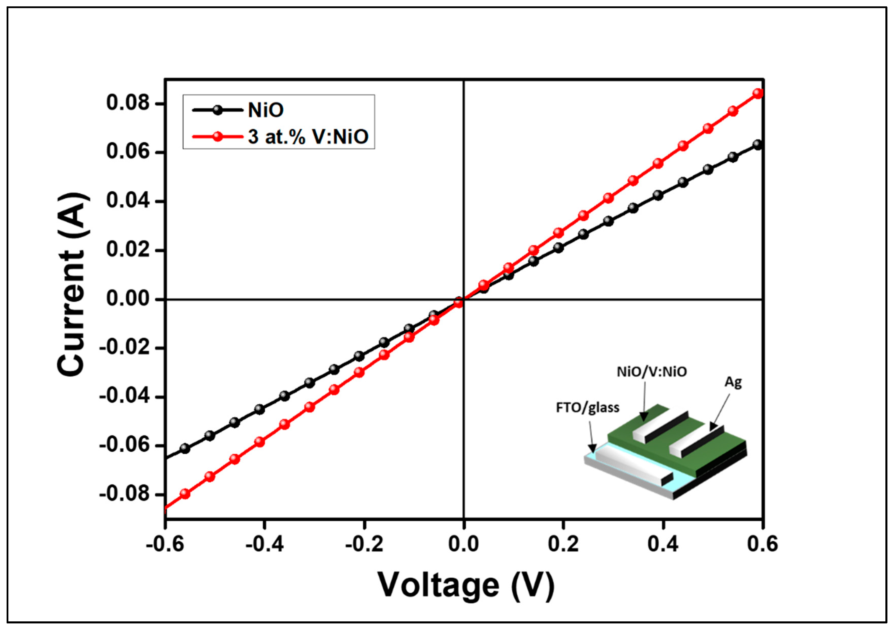
3.2. Study of Film Properties

The morphology of the surface of thin films of pristine NiO and 3 at.%V:NiO was studied using atomic force microscopy. Figure 6a–d shows AFM topography and three-dimensional (3D) images of NiO and 3 at.%V:NiO on FTO substrates. A clear observation of particle size reduction was also confirmed by the AFM topographic images of 3 at.%V:NiO film. Both the pristine and 3 at.%V:NiO films showed a closely packed uniform morphology and exhibited root mean square (RMS) surface roughness values of 2.94 nm and 2.49 nm, respectively. This reduction in surface roughness in the film after doping indicates that a small amount of vanadium in the NiO lattice will be beneficial for the various transparent conductive oxide applications [1,17,20,22].
We also investigated the influence of V doping on the electrical conductivity of the NiO thin films by a photovoltaic measurement system. For that, 20 mg/mL NiO or 3 at.%V:NiO dispersed in DI water was spin-coated onto a precleaned FTO substrate (16 Ω). Then, the substrates were annealed at 60 °C for 10 min to remove residual water. The electrodes were then transferred into a thermal evaporator (JVAC, South Korea) for the deposition of silver. The silver electrode (active area 0.2 cm2) was thermally evaporated with a thickness of 100 nm at a deposition rate of 0.4 nm per second through a shadow mask. The current–voltage (I–V) curves of the fabricated FTO/NiO and 3 at.%V:NiO/Ag films were measured by a source meter. The following equation used to calculate the conductivity of the films:
σ = d A × R
where σ is the conductivity, d is the thickness of the films, A is the active area, and R is the resistance obtained from the I–V curve. As shown in Figure 7, replacing the pristine NiO film with a 3 at.%V:NiO film significantly increased the vertical current, indicating the enhancement of electrical conductivity upon V doping. The conductivity values of the pristine NiO and 3 at.%V:NiO films were estimated to be 2.9 × 10⁻⁶ Scm−1 and 3.9 × 10⁻⁶ Scm−1, respectively. The conductivity of 3 at.%V:NiO film, compared to that of pristine NiO film, was enhanced by about 34.4% due to the enrichment of Ni3+ ions in the 3 at.%V:NiO sample [25]. This point was extensively discussed in the XPS analysis. The previously reported values are within the range for NiO films depending on the film composition and deposition condition [32]. A recent work by Julien et al. observed the same trend of an increase in conductivity for nitrogen-doped NiO film (2.8 × 10⁻⁷ Scm−1) compared to pristine NiO film (1.39 × 10⁻⁷ Scm−1) [26]. Our results demonstrate that V doping can be a powerful way to control the electrical conductivity of NiO.

4. Conclusions

In conclusion, pristine NiO and 3 at.% vanadium (V)-doped NiO were successfully synthesized by a solvothermal decomposition method and deposited on an FTO substrate. The 3 at.%V:NiO film exhibited a lower crystalline size when compared to pristine NiO film. A systematic crystallographic, optical, and morphological investigation showed that the V content in the NiO lattice would be beneficial for optoelectronic device applications. Also, AFM investigations of the 3 at.%V:NiO showed that the root mean square (RMS) surface roughness was lowered in comparison to that of the pristine NiO film. Finally, I–V curves showed that the conductivity of the V:NiO film was effectively enhanced by about 34.4%. The improvement of electrical conductivity can promote better charge transport and a reduction of interfacial charge accumulation.

Author Contributions

A.K. performed the experiments and wrote the manuscript. H.K.S. contributed to the preparation and revision of the manuscript. All authors have read and agreed to the published version of the manuscript.

Funding

This work was supported by a National Research Foundation of Korea (NRF) Project #2018 R1A4A102552813 and Korea Basic Science Institute (National research Facilities and Equipment Center) grant funded by the Ministry of Education (grant 2020R1A6C101A204).

Conflicts of Interest

The authors declare no conflict of interest.

References

  1. Zheng, J.; Hu, L.; Yun, J.S.; Zhang, M.; Lau, C.F.J.; Bing, J.; Deng, X.; Ma, Q.; Cho, Y.; Fu, W.; et al. Solution-Processed, Silver-Doped NiO x as Hole Transporting Layer for High-Efficiency Inverted Perovskite Solar Cells. ACS Appl. Energy Mater. 2018, 1, 561–570. [Google Scholar] [CrossRef]
  2. Hu, L.; Peng, J.; Wang, W.; Xia, Z.; Yuan, J.; Lu, J.; Huang, X.; Ma, W.; Song, H.; Chen, W.; et al. Sequential Deposition of CH3NH3PbI3 on Planar NiO Film for Efficient Planar Perovskite Solar Cells. ACS Photonics 2014, 1, 547–553. [Google Scholar] [CrossRef]
  3. Zhai, Z.; Huang, X.; Xu, M.; Yuan, J.; Peng, J.; Ma, W. Greatly Reduced Processing Temperature for a Solution-Processed NiO x Buffer Layer in Polymer Solar Cells. Adv. Energy Mater. 2013, 3, 1614–1622. [Google Scholar] [CrossRef]
  4. Im, H.C.; Choo, D.C.; Kim, T.W.; Kim, J.H.; Seo, J.H.; Kim, Y.K. Highly efficient organic light-emitting diodes fabricated utilizing nickel-oxide buffer layers between the anodes and the hole transport layers. Thin Solid Films 2007, 515, 5099–5102. [Google Scholar] [CrossRef]
  5. Amin, S.; Tahira, A.; Solangi, A.; Mazzaro, R.; Ibupoto, Z.H.; Vomiero, A. A sensitive enzyme-free lactic acid sensor based on NiO nanoparticles for practical applications. Anal. Methods 2019, 11, 3578–3583. [Google Scholar] [CrossRef]
  6. Vijayakumar, S.; Nagamuthu, S.; Muralidharan, G. Supercapacitor studies on NiO nanoflakes synthesized through a microwave route. ACS Appl. Mater. Interfaces 2013, 5, 2188–2196. [Google Scholar] [CrossRef]
  7. Seo, S.; Park, I.J.; Kim, M.; Lee, S.; Bae, C.; Jung, H.S.; Park, N.G.; Kim, J.Y.; Shin, H. An ultra-thin, un-doped NiO hole transporting layer of highly efficient (16.4%) organic-inorganic hybrid perovskite solar cells. Nanoscale 2016, 8, 11403–11412. [Google Scholar] [CrossRef]
  8. Natarajan, C.; Matsumoto, H.; Nogami, G. Improvement in electrochromic stability of electrodeposited nickel hydroxide thin film. J. Electrochem. Soc. 1997, 144. [Google Scholar] [CrossRef]
  9. Song, X.; Gao, L. Facile synthesis of polycrystalline NiO nanorods assisted by microwave heating. J. Am. Ceram. Soc. 2008, 91, 3465–3468. [Google Scholar] [CrossRef]
  10. Šurca, A.; Orel, B.; Pihlar, B.; Bukovec, P. Optical, spectroelectrochemical and structural properties of sol-gel derived Ni-oxide electrochromic film. J. Electroanal. Chem. 1996, 408, 83–100. [Google Scholar] [CrossRef]
  11. Wang, W.N.; Itoh, Y.; Lenggoro, I.W.; Okuyama, K. Nickel and nickel oxide nanoparticles prepared from nickel nitrate hexahydrate by a low pressure spray pyrolysis. Mater. Sci. Eng. B Solid-State Mater. Adv. Technol. 2004, 111, 69–76. [Google Scholar] [CrossRef]
  12. Qiu, Z.; Gong, H.; Zheng, G.; Yuan, S.; Zhang, H.; Zhu, X.; Zhou, H.; Cao, B. Enhanced physical properties of pulsed laser deposited NiO films via annealing and lithium doping for improving perovskite solar cell efficiency. J. Mater. Chem. C 2017, 5, 7084–7094. [Google Scholar] [CrossRef]
  13. Bai, Y.; Chen, H.; Xiao, S.; Xue, Q.; Zhang, T.; Zhu, Z.; Li, Q.; Hu, C.; Yang, Y.; Hu, Z.; et al. Effects of a Molecular Monolayer Modification of NiO Nanocrystal Layer Surfaces on Perovskite Crystallization and Interface Contact toward Faster Hole Extraction and Higher Photovoltaic Performance. Adv. Funct. Mater. 2016, 26, 2950–2958. [Google Scholar] [CrossRef]
  14. Sun, J.; Lu, J.; Li, B.; Jiang, L.; Chesman, A.S.R.; Scully, A.D.; Gengenbach, T.R.; Cheng, Y.B.; Jasieniak, J.J. Inverted perovskite solar cells with high fill-factors featuring chemical bath deposited mesoporous NiO hole transporting layers. Nano Energy 2018, 49, 163–171. [Google Scholar] [CrossRef]
  15. Zhang, H.; Cheng, J.; Lin, F.; He, H.; Mao, J.; Wong, K.S.; Jen, A.K.Y.; Choy, W.C.H. Pinhole-free and surface-nanostructured niox film by room-Temperature solution process for high-performance flexible perovskite solar cells with good stability and reproducibility. ACS Nano 2016, 10, 1503–1511. [Google Scholar] [CrossRef] [PubMed]
  16. Yin, X.; Chen, P.; Que, M.; Xing, Y.; Que, W.; Niu, C.; Shao, J. Highly Efficient Flexible Perovskite Solar Cells Using Solution-Derived NiOx Hole Contacts. ACS Nano 2016, 10, 3630–3636. [Google Scholar] [CrossRef]
  17. Liu, S.; Liu, R.; Chen, Y.; Ho, S.; Kim, J.H.; So, F. Nickel oxide hole injection/transport layers for efficient solution-processed organic light-emitting diodes. Chem. Mater. 2014, 26, 4528–4534. [Google Scholar] [CrossRef]
  18. He, Q.; Yao, K.; Wang, X.; Xia, X.; Leng, S.; Li, F. Room-Temperature and Solution-Processable Cu-Doped Nickel Oxide Nanoparticles for Efficient Hole-Transport Layers of Flexible Large-Area Perovskite Solar Cells. ACS Appl. Mater. Interfaces 2017, 9, 41887–41897. [Google Scholar] [CrossRef]
  19. Chen, W.; Liu, F.-Z.; Feng, X.-Y.; Djurišić, A.B.; Chan, W.K.; He, Z.-B. Cesium Doped NiO x as an Efficient Hole Extraction Layer for Inverted Planar Perovskite Solar Cells. Adv. Energy Mater. 2017, 7, 1700722. [Google Scholar] [CrossRef]
  20. Jung, J.W.; Chueh, C.C.; Jen, A.K.Y. A Low-Temperature, Solution-Processable, Cu-Doped Nickel Oxide Hole-Transporting Layer via the Combustion Method for High-Performance Thin-Film Perovskite Solar Cells. Adv. Mater. 2015, 27, 7874–7880. [Google Scholar] [CrossRef]
  21. Sun, X.; Li, B.; Metiu, H. Ethane activation by Nb-doped NiO. J. Phys. Chem. C 2013, 117, 23597–23608. [Google Scholar] [CrossRef]
  22. Hu, Z.; Chen, D.; Yang, P.; Yang, L.; Qin, L.; Huang, Y.; Zhao, X. Sol-gel-processed yttrium-doped NiO as hole transport layer in inverted perovskite solar cells for enhanced performance. Appl. Surf. Sci. 2018, 441, 258–264. [Google Scholar] [CrossRef]
  23. Jun-Dar, H.; Wang-Ting, H.; Bo-Yu, L.; Yu-Ting, H.; Shr-Ting, W. Effect of Ag-doping on the characteristics of AgxNi1-xO transparent conducting oxide film and their applications in heterojunction diodes. J. Phys. D Appl. Phys. 2020, 53, 275107. [Google Scholar]
  24. Sharma, R.; Yadav, K. Effect of lattice defects on the structural and optical properties of Ni1—XAgXO (where X = 0.0, 0.01, 0.03, 0.05, 0.10 and 0.15) nanoparticles. Appl. Phys. A Mater. Sci. Process. 2018, 124. [Google Scholar] [CrossRef]
  25. Xie, Y.; Lu, K.; Duan, J.; Jiang, Y.; Hu, L.; Liu, T.; Zhou, Y.; Hu, B. Enhancing Photovoltaic Performance of Inverted Planar Perovskite Solar Cells by Cobalt-Doped Nickel Oxide Hole Transport Layer. ACS Appl. Mater. Interfaces 2018, 10, 14153–14159. [Google Scholar] [CrossRef]
  26. Keraudy, J.; Ferrec, A.; Richard-Plouet, M.; Hamon, J.; Goullet, A.; Jouan, P.Y. Nitrogen doping on NiO by reactive magnetron sputtering: A new pathway to dynamically tune the optical and electrical properties. Appl. Surf. Sci. 2017, 409, 77–84. [Google Scholar] [CrossRef]
  27. Chen, P.C.; Yang, S.H. Potassium-Doped Nickel Oxide as the Hole Transport Layer for Efficient and Stable Inverted Perovskite Solar Cells. ACS Appl. Energy Mater. 2019, 2, 6705–6713. [Google Scholar] [CrossRef]
  28. Islam, M.B.; Yanagida, M.; Shirai, Y.; Nabetani, Y.; Miyano, K. NiO x Hole Transport Layer for Perovskite Solar Cells with Improved Stability and Reproducibility. ACS Omega 2017, 2, 2291–2299. [Google Scholar] [CrossRef] [Green Version]
  29. Kwon, U.; Kim, B.-G.; Nguyen, D.C.; Park, J.-H.; Ha, N.Y.; Kim, S.-J.; Ko, S.H.; Lee, S.; Lee, D.; Park, H.J. Solution-Processible Crystalline NiO Nanoparticles for High-Performance Planar Perovskite Photovoltaic Cells. Sci. Rep. 2016, 6, 30759. [Google Scholar] [CrossRef] [Green Version]
  30. AlFaify, S.; Shkir, M. A facile one pot synthesis of novel pure and Cd doped PbI2 nanostructures for electro-optic and radiation detection applications. Opt. Mater. 2019, 88, 417–423. [Google Scholar] [CrossRef]
  31. Geng, X.; Lahem, D.; Zhang, C.; Li, C.-J.; Olivier, M.-G.; Debliquy, M. Visible light enhanced black NiO sensors for ppb-level NO2 detection at room temperature. Ceram. Int. 2019, 45, 4253–4261. [Google Scholar] [CrossRef]
  32. Xia, X.; Jiang, Y.; Wan, Q.; Wang, X.; Wang, L.; Li, F. Lithium and Silver Co-Doped Nickel Oxide Hole-Transporting Layer Boosting the Efficiency and Stability of Inverted Planar Perovskite Solar Cells. ACS Appl. Mater. Interfaces 2018, 10, 44501–44510. [Google Scholar] [CrossRef] [PubMed]
Scheme 1. Synthesis of V:NiO nanoparticles by solvothermal decomposition of a V:Ni-oleylamine complex.
Applsci 10 05415 sch001
Figure 1. (a) XRD spectra of pristine and 3 at.%V:NiO nanoparticles (NPs) and (b) enlarged XRD spectra of pristine NiO and 3 at.%V:NiO NPs.
Applsci 10 05415 g001
Figure 2. (a) FTIR spectra of NiO and 3 at.%V:NiO with precursor materials, (b) EDS spectra of 3 at.%V:NiO NPs, and (c) EDS elemental mapping of the corresponding elements of Ni, O, and V (scale bar, 2 μm).
Applsci 10 05415 g002
Figure 3. (a) Raman spectra of NiO and 3 at.%V:NiO NP powder samples; (b) UV-absorption spectra of diluted NiO and V:NiO NP solutions with different atomic percentages of V; (c) Corresponding Tauc plots of the absorption spectra; (d) Optical transmission spectra of NiO and V:NiO films with different atomic percentages of V.
Applsci 10 05415 g003
Figure 4. (a) FESEM images of (a) NiO and (b) 3 at.%V:NiO and TEM patterns of (c) NiO and (d) 3 at.%V:NiO. (e,f) HRTEM images of both (e) NiO and (f) 3 at.%V:NiO and (g) statistics of the particle distributions of NiO and 3 at.%V:NiO NPs.
Applsci 10 05415 g004
Figure 5. (ac) XPS spectra of NiO: (a) survey spectra (inset: high-resolution spectra of V 2p), high-resolution (b) Ni 2p3/2 and (c) O 1s; (df) XPS spectra of 3 at.%V:NiO: (a) survey spectra (inset: high-resolution spectra of V 2p), high-resolution (b) Ni 2p3/2 and (c) O 1s.
Applsci 10 05415 g005
Figure 6. AFM topography and 3D AFM images of (a,b) NiO NPs and (c,d) 3 at.%V:NiO.
Applsci 10 05415 g006
Figure 7. I–V curves of NiO and 3 at.%V:NiO films based on the structure of FTO/NiO or 3 at.%V:NiO/Ag; the inset shows the corresponding fabricated electrode structure.
Applsci 10 05415 g007
Table 1. Measured values of structural parameters for NiO and V:NiO.
Samples2θ (°)hklFWHMdsp (A°)Dp (nm)δ (nm−1)ε × 10−2
NiO43.2512002.942.0953.040.10820.955
3 at.%V:NiO43.2782003.172.0942.820.12571.054

