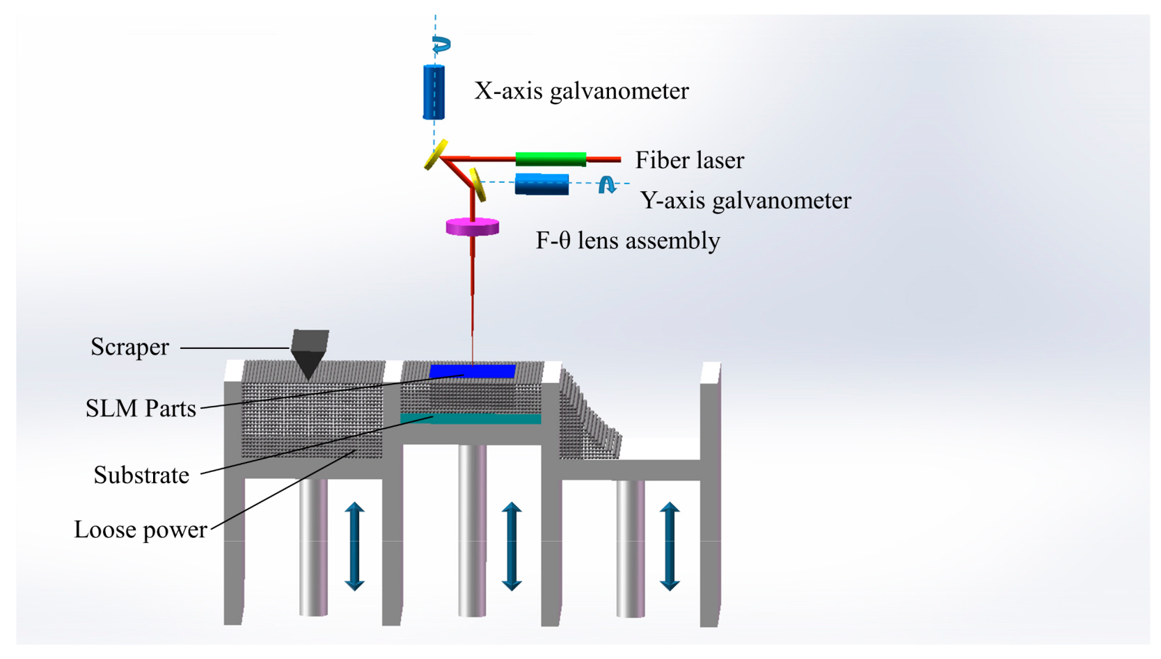
Article

Microstructure and Tensile Properties of AlSi10Mg Alloy Manufactured by Multi-Laser Beam Selective Laser Melting (SLM)

1
School of Mechanical Engineering, North University of China, Taiyuan 030051, China
2
School of Materials Science and Engineering, North University of China, Taiyuan 030051, China
3
State Key Laboratory of Mechanical Transmissions, Chongqing University, Chongqing 400044, China
*
Authors to whom correspondence should be addressed.
These authors contributed equally to this work.
Metals 2019, 9(12), 1337; https://doi.org/10.3390/met9121337
Submission received: 17 October 2019 / Revised: 29 November 2019 / Accepted: 4 December 2019 / Published: 11 December 2019

Abstract

:
The multi-beam selective laser forming system is a new type of powder bed laser forming equipment that is different from single-laser selective laser melting (SLM) printers. It is a new generation for a metal powder material moulding process that has high efficiency, large size and batch manufacturing. It is a new development of a powder bed laser forming process trend. In this paper, the microstructure and tensile properties of both the multi-laser-formed AlSi10Mg isolated and overlap areas are studied to ensure that the parts can achieve perfect seamless splicing and to identify whether the parts in different regions have the same performance. It was discovered that as the number of scans increases, the depth and width of the melt pool and microscopic grain structure in the overlap zone increase. The preferential crystallite growth orientation reaches the (200) plane. A small amount of smooth surface appeared at the fracture of the overlap area of the two scans, the dimples were reduced and the structure became larger, resulting in a decrease in tensile properties.

1. Introduction

AlSi10Mg is a widely used alloy with high corrosion resistance and low density. It has good solderability, castability, hardenability and good antistatic and dynamic properties. AlSi10Mg alloy is widely used in aviation, aerospace, automotive, machinery manufacturing, shipbuilding, chemical and other industrial fields [1,2]. With the rapid development of economic and social production and the pursuit of higher product performance, the demand for aluminium alloys is increasing, which means the research into its performance is becoming a hotspot for researchers. The Al–Si alloy also has good weldability and is suitable for laser processing.
SLM technology is an additive manufacturing technique in which metal powder is completely melted under the action of the heat of a laser beam and solidified by cooling [3]. SLM is a promising additive manufacturing process that has the advantage of forming complex geometries [4]. SLM uses a high-energy laser beam to selectively melt metal powder and directly form dense metal parts, as shown in Figure 1. SLM uses the principle of discrete-stacking to produce metal according to the 3D CAD slice model of the part. The powder layer-by-layer deposition is superimposed into a three-dimensional object, which can form complex parts quickly and cost-effectively, to realise the individualisation, as well as small batch productions. However, the current SLM process is not fully capable of meeting the serial production and manufacturing efficiency requirements of large-scale components. The most efficient way to increase the rate of the laser forming process is to match thicker powder layers at higher scan speeds and higher laser power conditions. Currently, there are three main strategies to improve the building efficiency, which include using internal multi-layer filling, increasing the scanning speed and the thickness of the powder layer under high laser power and increasing the number of laser scanning heads [5]. The first method is to reduce the internal filling scan time. The device is equipped with a dual laser (small spot low-power fibre laser + large spot high-power fibre laser), which scans the outer shell of the part through a small spot fibre laser, after forming the N layer. The large-spot fibre laser is used to scan the inner core, and the N-layer inner core is directly formed by high power, thereby improving the forming efficiency. The second method to increase the scanning speed and the thickness of the powder layer is under high laser power. However, increasing the laser power causes the laser spot diameter to increase which may affect the accuracy and, therefore, the physical and mechanical properties of the part. The third way is to increase the number of laser heads in the same forming size space, thereby rapidly improving the efficiency. This technology is most commonly used by equipment manufacturers to improve scanning efficiency through multi-laser head partitioning. During the partitioning, the two galvanometers are responsible for the intersection of the areas being scanned. According to the working conditions, the two galvanometers of the current layer are responsible for the scanning area of the area compared to the smaller galvanometer, and bear the cross-region scanning. It has become a research objective to develop a multi-beam matching forming process and improve forming efficiency to achieve multi-beam matching and high-precision additive manufacturing [6].
Multi-laser beam machining is an effective way to increase the size and efficiency of SLM moulded parts. Multi-laser SLM technology can effectively increase forming speed, reduce moulding time, and produce parts with larger geometries. Wang Zemin et al. [7] studied the microstructure and mechanical properties of the four laser-fabricated Ti6Al4V overlap areas and isolated areas using self-developed multi-laser equipment. The results illustrated that the stair-step phenomenon of the overlap areas can be eliminated by the compartment rotation scan, and also there was no significant change in the microstructure and mechanical properties of the overlap areas. Wiesner et al. [8] used the SLM 500 HL multi-laser device to produce large cylinder heads, each with dimensions 494 × 210 × 143 mm. The manufacturing time was reduced from 170 h for dual lasers to 85 h for four lasers, and the production efficiency was greatly improved. This both highlights an important breakthrough in multi-laser SLM additive manufacturing and proves that multi-laser SLM manufacturing has significant advantages. Buchbinder et al. [9] used a new prototype machine tool, including a 1 kW laser and a multi-beam system, to improve the efficiency of aluminium alloy. Heeling et al. [10,11] studied the effect of the laser compensation process on the stability of SLM formation. This study discovered that the two lasers work together with the melt pool and the proper power compensation, and focusing the positioning of the second laser can more accurately control the laser melting process. This helps stabilise the melt pool, obtain dense parts, reduce temperature gradients, and reduce residual stress. Weingarten et al. [12] used just one beam, however they scanned the part two times to dry the aluminium powder bed in the process, prior to melting, to reduce the amount of hydrogen porosity. Abe et al. [13] used a second moving beam in a simple test to selectively reduce the cooling rates and thus influence the microstructure with promising results.
However, research on multi-laser SLM forming parts has rarely been reported. There are few studies that have been published on the performance consistency of multi-laser SLM forming AlSi10Mg. In this paper, the double-laser overlap area, the four-laser overlap area and the isolated area in the microstructure, phase change will be studied, and will analyse the change mechanism.

2. Materials and Methods

Multi-laser forming is achieved by simulation of a single laser device (Renishaw AM-400, Renishaw, Wotton-under-Edge, UK). The machine is equipped with a modulated ytterbium fibre laser with a wavelength of 1070 nm. This project uses Quant AM software to splice two or four parts, and the overlapping area will be repeatedly melted under the set process to achieve multi-laser bonding, as shown in Figure 2a. The double-laser overlap area is equivalent to the laser repeating the scanning of one area two times, and the same four-laser overlap area is equivalent to repeating the scanning four times. A single laser device (Renishaw AM-400, Renishaw, Wotton-under-Edge, UK) scans one, two, and four times per layer to achieve single laser, double laser, and four laser formed parts respectively. The experiment design of multi-laser manufacturing is shown in Figure 2b. The sizes of the samples are 10(L) × 10(W) × 10(H) mm and the two other formed samples are 15(L) × 10(W) × 10(H) mm. The area with an intermediate size of 5(L) × 10(W) mm is a double laser and a four-laser overlapping area, respectively. The top surface morphology of the samples is presented in Figure 3. Optimised processing parameters (laser power: 200 W, scanning distance: 80 µm, layer thickness: 25 µm, spot diameter: 80 µm, exposure time: 140 µs, and point distance: 80 µm) were used in this study. The scanning direction is shown in Figure 2c.
The AlSi10Mg powder used in this study was provided by LPW Technology (LPW Technology Ltd., Widnes, Cheshire, UK). As shown in Figure 2d, the powder is prepared by gas atomisation and has a spherical shape. The average particle size was 45 μm, obeying normal distribution and having good flowability. The chemical composition of the powder is shown in Table 1.
The as-built specimens were removed from the aluminium base plate by wire EDM cutting. Keller’s reagent was used to etch polished specimens. The phase identification was identified through an X’Pert—Pro X-ray diffractometer (D/max-rB, Rigaku Corporation, Tokyo, Japan). The XRD test used working power 10 kW, working current 250 mA, working voltage 40 kV, step size 0.02°, scanning speed 5°/min, and scanning range 20–90°. A Zeiss optical microscope (OM) (Axio Scope A1, Carl Zeiss, Jena, Germany) for low-magnification, a Hitachi SU-5000 scanning electron microscopy (SEM) (SU-5000SEM, Hitachi Ltd., Chiyoda-ku, Tokyo, Japan) and a Tescan VEGA3 scanning electron microscopy (SEM) (VEGA3 SEM, Tescan China, Ltd., Brno, Czech Republic) for high magnification were used to observe the microstructures of samples. The elemental analysis was investigated using an energy-dispersive spectrometer (EDS), which was performed on the SEM device. Tensile properties of this experiment were tested using a microcomputer-controlled electronic universal testing machine (CMT5105, MTS Industrial Systems (China) Co. Ltd., Shenzhen, China). Tensile samples in isolated areas and overlap areas were built according to Figure 4 in this experiment. The overlap width of the tensile samples is 1 mm. The overlap areas of the tensile samples were scanned twice. The tensile speed of the pattern is 0.02 mm/s. Each mechanical property data is the average of two valid data.

3. Results

3.1. Microstructure

In the conventional cast Al–Si hypoeutectic alloy [14], since the solidification process is non-directional solidification, the primary alpha-Al dendrites do not have the characteristics of directional growth, and there is no fixed dendrite spacing, however, the dendrite size is an order of magnitude larger than the SLM formation. SLM is a process of rapid melting and solidification, and the solidification rate of its molten pool is fast (up to 106–108 °C/s), and the alloy obtained has ultra-fine grain size, thus presenting a series of different microstructure and structure characteristics from conventional alloy.
Figure 5b shows the morphology of the microstructure of one scan. The layers of the weld line are overlapped and the shape is clearly visible. The red dotted line in the figure is the boundary of the molten pool where the dendrites are thicker than the inside of the molten pool and grow in a cell shape with an average primary dendrite spacing λ1 of 1.5 µm; the internal dendrites are relatively small and grow in dendrites, with an average primary dendrite spacing λ1 of less than 1 µm. The dendrites have a typical epitaxial growth characteristic, that is, the branches grow to the top along the bottom of the molten pool, although there are sub-structures in which the dendrite growth directions are inconsistent at local locations in the same molten pool. Figure 5c is a microscopic diagram of the two scans where the red dotted line is the boundary of the molten pool, which becomes larger. Figure 5d shows the microstructure of four scans from which it can be seen that the boundary of the molten pool becomes linear and blurred.
According to the solidification principle of Al–Si binary phase diagram, the alloy first undergoes precipitation of the primary alpha Al phase during solidification, that is, L→L+α, then the temperature reaches the eutectic point (577 °C) and the eutectic reaction L→α+Si occurs. According to the solidification process of AlSi10Mg, the dendrites (cell crystals, dendrites) described above are primary alpha Al, that is, the bright regions in Figure 5, when the temperature reaches the eutectic point, Al– precipitates between the dendrites. Si eutectic structure, which is the dark region of Figure 5, but the orientation of the dendrite growth direction determines the precipitation morphology of the Al–Si eutectic structure, resulting in anisotropy of the microstructure of the alloy in different directions.
Figure 6 shows the top surface microstructure of the SLM-formed AlSi10Mg alloy. In Figure 6a–c, the formation of the melting trajectory can be seen. The upper and lower layers observe the bidirectional laser scanning trajectory, and the upper strip or cylindrical fine blister structure is solidified. The reason for the melting trajectory is that since the raw material for SLM forming is a spherical powder, the spherical powder generates a liquid phase and spreads out in the process of absorbing laser energy and melting. It can be seen from the melting trajectory of the lower layer that the laser spot is formed into a line, and the tightly melted plane between the line and the line is relatively flat, indicating that the process parameters of the SLM process are accurate and no large holes nor looseness are observed, which also indicates that the powder has good fluid flow performance. The porosity between the powders is low and the density is higher after the laser is melted and formed. It can be seen from Figure 6d–f that a coarse crystal region is formed at the boundary of the molten pool region, mainly coarse cell crystal. The reason for this formation is mainly due to the re-melting of the solidified alloy by the laser scanning line, so that the solidified alloy re-crystallises, and the crystal grains grow again and form a coarse crystal region. A fine-grained zone is formed in the centre of the molten pool zone, mainly composed of finely dispersed cell crystals. The reason for the formation is mainly due to the temperature gradient in the centre of the molten pool area, which is the smallest, the solute distribution is relatively uniform, and the supercooling degree is formed at the front edge of the interface, which generates a large number of crystal nuclei, and the rapid solidification inhibits the growth of the crystal grains, thereby forming a fine grain area [3,15]. The other side of the coarse grain zone is the heat affected zone, mainly coarse particles. Combined with the XRD analysis (Figure 7), the particles can be judged to be coarse eutectic Si. The reason for the formation is mainly because the position of the solidified region close to the coarse crystal region is affected by the heat transfer of the laser scanning line, and the chaos of the eutectic Si is increased to form a self-shaped crystal. In the fine-grained zone inside the molten pool, the Al–Si eutectic structure precipitates between the alpha Al dendrites, and its morphology is a fine network structure with a width of <1 µm. The primary alpha Al phase is Al–Si eutectic. Surrounding this is the coarse-grained zone is located at the boundary of the molten pool. Since the primary α-Al grows here in the form of cell crystals, the morphology of the Al–Si eutectic structure is a nearly circular network with a width between 1 and 3 µm. It can be seen that the Al–Si eutectic structure at the boundary of the molten pool is clearly roughened when compared with the inside of the molten pool. The heat affected zone (HAZ) is located outside the molten pool, and the laser is formed by the secondary heating of the laser during the scanning process of the previous layer. The cycle causes the Al–Si eutectic structure to be decomposed, the network Al–Si eutectic structure is gradually interrupted, and the morphology is close to the spherical particles [16].
It can be seen from the Figure 6d–f that as the number of laser scans increases, the grain structure becomes larger. This is because as the number of scans increases, the temperature of the molten pool rises, causing the cooling rate to slow down, thereby causing the grains to grow. As the number of scans increases, the solidified layer of the alloy re-crystallises and the grain grows. Thijs et al. [3] studied the effects of different scanning strategies on AlSi10Mg parts. The results illustrate that the high-energy gradient in the SLM process leads to submicron cells. The coagulation mode is active, and the preferential growth direction of the cells proceeds along the (100) crystal direction, towards the centre line of the molten pool. The face centred cubic aluminium cells are decorated by a diamond-like silicon phase. Therefore, we can infer that the fine crystals are formed in the molten pool, and begin to thicken near the centre until the boundary of the heat affected zone is reached. The laser is scanned multiple times to obtain re-crystallisation and a fine structure of the upper coarse structure.
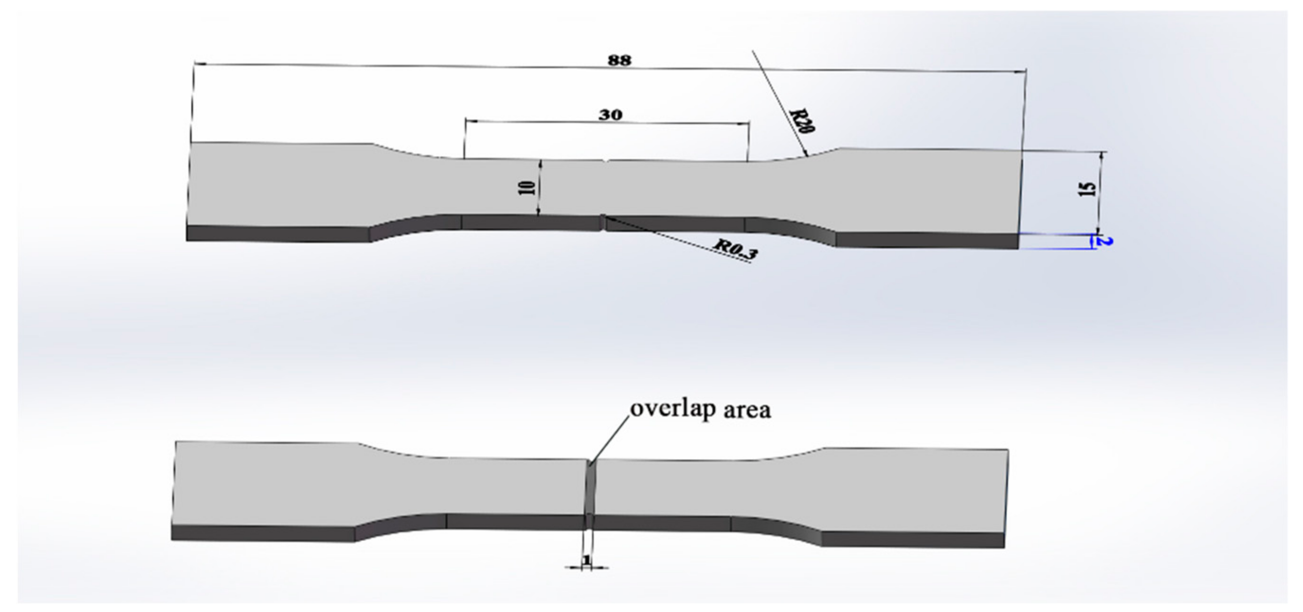
The laser focused spot that affects the width of the melt is generally related to the design of the laser used by the device. The heat affected zone of the energy is mainly affected by the laser power and the scanning speed. When the scanning speed is constant, the larger the laser power and the larger the energy heat affected zone. When the two lasers illuminate the overlap area, the laser energy input increases and the heat affected zone increases. Compared to the energy density of the second and four scans, it can be established that the heat affected zone increases and the corresponding melt width increases.
XRD patterns (Figure 7) show that the phase composition of α-Al and Si are found in both AlSi10Mg powders and AlSi10Mg samples (i.e., the microstructure was mainly composed of an Al/Si phase). It can be seen from the spectrum in the XRD that the peak of Al in the sample forming the SLM and the peak corresponding to the powder slightly moved to the right and moved to a higher angle. According to the basic principle of X-ray diffraction, there is a certain relationship between the diffraction angle (θ) corresponding to the diffraction peak and the interplanar spacing (d), which can be expressed by the Bragg relation:
2 d sin θ = n λ  
The XRD test used in the experiment uses a CuKa target, so the wavelength (λ) is 0.15406 nm. In addition, α-Al is a face-centred cubic structure, and the lattice constant at room temperature is 0.40495 mm. The interplanar spacing and lattice constant have the following equation:
d = a h 2 + k 2 + l 2
From Equation (1), it is understood that the diffraction angle 2θ becomes large, the sine value becomes large and the interplanar spacing D becomes small. From Equation (2), it is understood that the lattice constant (a) becomes small and it is understood that α-Al undergoes lattice distortion. During the forming process of AlSi10Mg, the process itself is carried out by laser beam scanning with a fast scanning speed. Therefore, the melting of the synthetic metal and the process of cooling and solidification are also fast, and the Si grains in the alloy are too late to precipitate and grow the alloy. It has been solidified and formed in a solid solution of Si in the matrix of Al to form a supersaturated solid solution. The α-Al matrix exists in the form of a replacement solid solution as the radius of the Al atom is 0.143 nm, which is a solvent atom, and the atomic radius of Si is 0.117 nm, which is a solute atom. Therefore, in the Al matrix, Si atoms in the crystal lattice occupy a large number of positions of Al atoms. Lattice distortion is generated, and the lattice constant of the Al matrix becomes small. The derivative peak corresponding to the Al matrix shifts to the right, which matches the results displayed in the figure.
No Mg2Si was found in the XRD pattern, which is consistent with previous studies on the AlSi10Mg alloy manufactured by SLM [17,18]. However, there are also some studies of Mg2Si for XRD detection [19,20]. This may be because the amount of Mg in AlSi10Mg is too small, which is lower than the detection ranges of the machine. As the number of laser scans increases, the rate of solidification also increases. As a result, a Si-formed solid solution is found in the Al matrix, and failed to precipitate in the form of primary silicon and eutectic silicon. This results in a decrease in the peak of Si and an increase in the peak of α-Al. The preferred orientation shown is the (200) plane. This texture is usually produced by preferential solidification in the (100) cube texture along the building direction [3,21]. This is related to the microstructure and texture characteristics of AlSi10Mg produced by the SLM process.
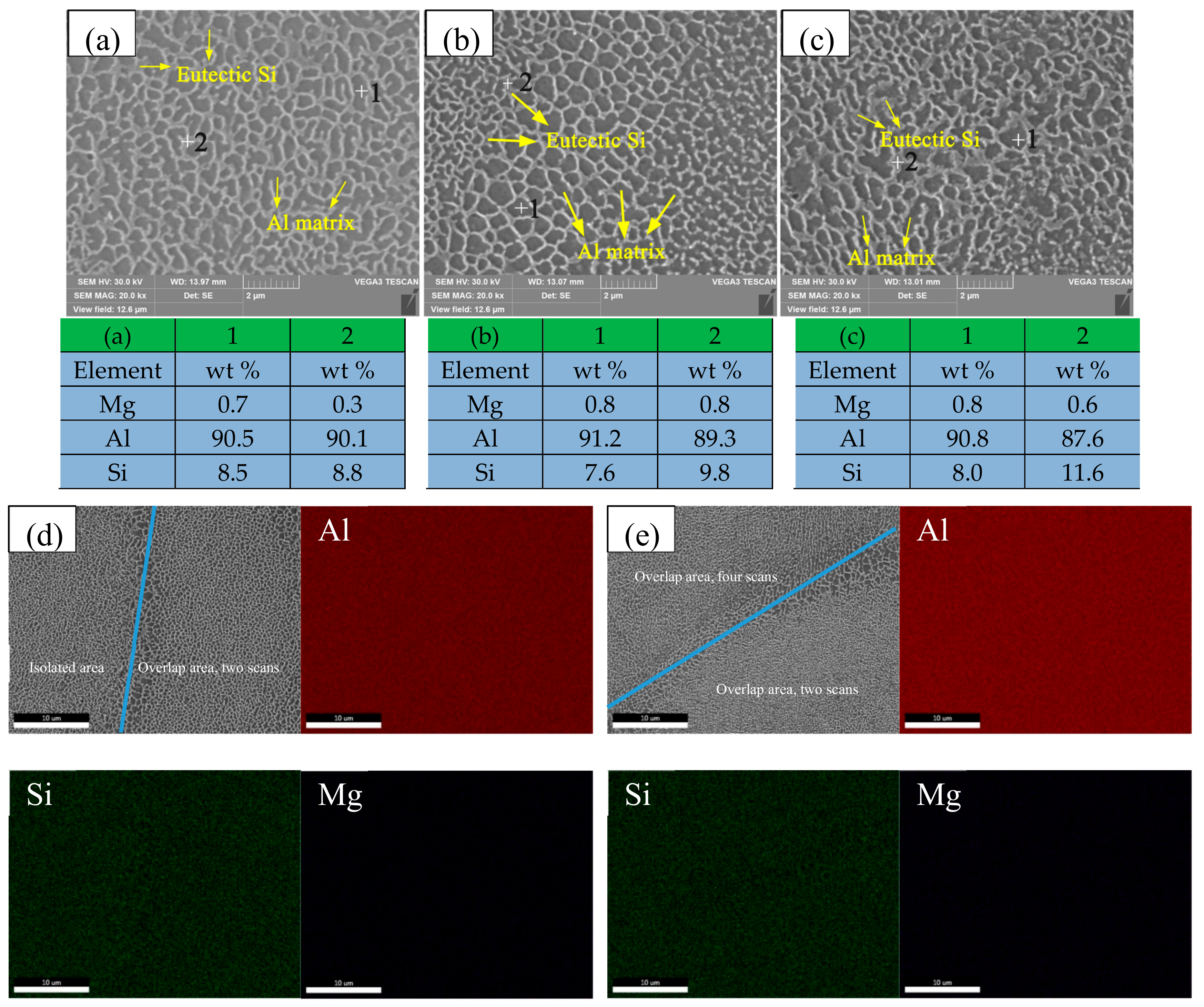
Figure 8 shows the SEM image of the cross section of the SLMed AlSi10Mg samples. The grey island-like regions are columnar dendritic α-Al matrixes, and the white mesh-like regions are eutectic precipitated Si phases. The Si phase is uniformly distributed in a network on the α-Al matrix. The factors leading to the appearance of this micro-morphology are mainly due to the rapid formation of liquid molten pools during SLM forming. The presence of convection causes the liquid phase in the molten pool to reach liquid phase equilibrium and each element is evenly distributed, and the Si element is evenly distributed in the Al matrix. During rapid cooling, the process of element segregation is suppressed, and grain growth is limited. Si will rapidly nucleate and grow in the Al matrix during rapid cooling. There are many Si atoms in the Al matrix and the distribution is uniform, so a small range of aggregation occurs to a certain extent. It can be seen from Figure 8a–c that there is no significant change in the element content of the samples in one scan, two scan, and four scan. It can be seen from Figure 8 that the Al, Si and Mg elements in the sample are uniformly distributed, and there is no macro-segregation. As can be seen from Figure 8d,e, the size of the lap area is relatively large, which is because the lap area has undergone two and four times of laser scanning, which is equivalent to remelting. There is thermal accumulation, and the grain has the opportunity to grow further. The distribution of Mg element is relatively uniform and there is no trend of enrichment. 
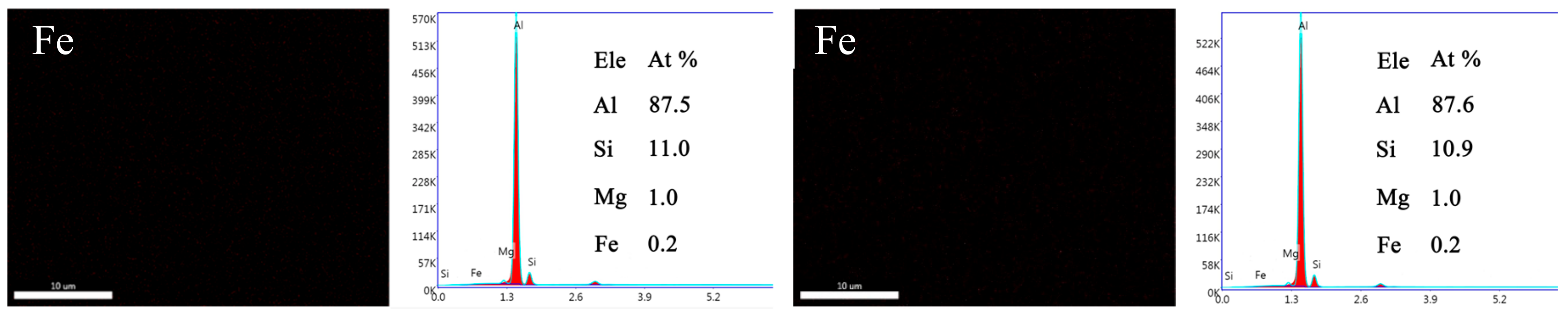
Figure 8d,e shows a field of view randomly selected by a scanning electron microscope and the area is scanned face-to-face, and the distribution of the Mg element of the Si element of the Al element of Fe element is listed. As can be seen from the distribution of the elements in the figure, in the selective laser melting of AlSi10Mg alloy, due to its extremely fast cooling rate, it can reach 103 K/s, and the element distribution is uniform at this cooling rate.
The solidification rate R and the thermal gradient G are the two most important coagulation scalars. The G/R ratio determines the solidification morphology, with higher G/R leading to cellular structure associated with most SLM processes. In the SLM process, the solidification mode and characteristic fineness depend on the thermal gradient G and the solidification rate R. The G/R ratio determines the fineness of the structure and is calculated by the following equation [22]:
  G R < Cst           E q u i a x e d   g r a i n s   G R > Cst           C o l u m n a r   g r a i n s
where Cst is the criterion of columnar to equiaxed transition. In addition, the G/R product, which represents the cooling rate, determines the size of the microstructure where the higher the G/R value the finer the structure. The ratio of G/R represents the cooling rate of the alloy. The higher the G/R value, the finer the structure. The bath boundary is maintained at a higher temperature for a longer period of time, so the cooling rate from the melt pool core to the edge is reduced. Different grain structures can be obtained by changing the process parameters to control the G and R values, where a higher G R ratio limits columnar growth [23]. The columnar grains originate from epitaxial grains grown in the direction of heat flux (generating direction) and can also be observed in the microstructure of directional solidification. Figure 9 illustrates that the microstructure of the vertical section is an elongated columnar dendrite, which is different from the cross section. The overlap area of the two laser scans has a small G/R value, resulting in a large tissue structure. Similarly, the overlapping area of the scanning of the four lasers has a larger columnar dendrite structure. The relationship between dendrite spacing and cooling velocity can be expressed as [21,24]:
  L = B R C n
where B is the proportionality constant. The results show that with the decrease of cooling rate Rc, the spacing between the twin crystal rods increases. It can be seen from Figure 9 that the microstructure in the overlap area has sufficient time for grain growth, therefore, the dendrite spacing increases. This also implies that the amount of Si rejected from the supersaturated Al increases.

3.2. Tensile Properties

In this experiment we mainly studied the tensile strength of the overlap areas of two laser scans, where Table 2 and Figure 10 shows the tensile properties of the samples in this work. As can be seen from Figure 10 the tensile curves of the samples are similar, and thus the tensile properties are not much different. The average ultimate tensile strengths, yield strength and elongation of isolated and overlap samples are 370 MPa, 360 MPa, 100 MPa, 95 MPa, 2.0% and 1.8%, respectively. The tensile strength and yield strength of the sample were good, but the elongation was low, indicating that the fracture toughness of the alloy was low. SLM is a high-speed melting and solidification process in which very small particles of structure are formed in the sample. Therefore, the strengthening of the AlSi10Mg alloy can generally be considered as grain refinement strengthening. Grain refinement can increase tensile strength and, according to the Hall–Petch theory, the grain refinement increases the number of crystal grains contained in the same volume, and the internal dislocations become less. When the part is subjected to an external force, the deformation occurs between a large number of crystal grains. Additionally, the slip of the dislocation is blocked by the grain boundary, so that the expansion cannot be continued, thereby achieving fine grain strengthening. Although the tensile properties of the sample scanned by the laser have decreased, the tensile properties variation is not particularly remarkable as the multi-laser overlap area tensile properties are the same as the isolated area.
Figure 10 is the stress-strain curve of an isolated sample and an overlap sample. The yield strength and tensile strength of the stretched part formed by one scan are slightly greater. After two scans, there was a slight increase in the elongation of the stretched part. In order to understand the influence of the multi-laser process on the properties of SLM AlSi10Mg alloy further, the fracture morphology of SLM AlSi10Mg alloy samples under different scanning times was analysed. Figure 11a–d show the fracture morphology of the standard samples at one scan and two scans, respectively. It can be seen from the Figure 11 that the fracture of the AlSi10Mg tensile specimen formed by SLM is a typical inter-granular fracture, and there are very shallow dimples at the fracture, indicating that the toughness of the specimen is poor, mainly brittle fracture. A small number of circular pores are caused by the rapid melting and cooling of the gas during the SLM process, which is wrapped in the molten pool. It can be seen from Figure 11b,d that the microstructure becomes coarse after two scans, so that the yield strength and tensile strength of the part will decrease.

4. Conclusions

The microstructure of overlap area is slightly different from that of the isolated area. By observing the front plane of the samples, the sample that has been formed by one laser scan can see a relatively apparent fish-scale melt pool boundary. However, the melt pool boundary of overlap areas is not as clear as when the number of scans increases the higher the number and, therefore, the less apparent. As the number of laser scans increases, the grain structure becomes larger. This is because as the number of scans increases, the temperature of the molten pool rises, causing the cooling rate to slow down, thereby causing the grains to grow. As the number of scans increases, the solidified layer of the alloy recrystallizes and the grain grows. Compared to the energy density of the second and four scans, it can be established that the heat affected zone increases and the corresponding melt width increases. The elements in the overlap area and the isolated area are evenly distributed, and there is no macro-segregation. The microstructure of the junction between the overlap area and the isolated area becomes larger.
It can be seen from the spectrum in XRD that the peak of Al in the SLM sample and the peak corresponding to the powder are shifted to the right. As the number of laser scans increases, the preferential crystallite growth orientation reaches the (200) plane.
The tensile properties of the samples with different scanning times changed slightly. The tensile strength and yield strength of the stretched part formed by two scans is slightly lower than that of the stretched part formed by one scan. By observing the SEM fractograph of tensile fracture, it was established that the microstructure become larger at the fracture of the overlap area of the two scan, which resulted in a decrease in tensile strength and yield strength.

Author Contributions

Supervision: P.B.; formal analysis: Y.N.; investigation: Z.K. and Y.N.; validation: G.F.; methodology: W.L. and S.Y.; writing—original draft: Z.L.; writing—review and editing: Z.K.

Funding

This research was funded by the National Natural Science Foundation of China (grant no. 51905497), the Major Science and Technology Projects of Shanxi Province, China (no. 20181102012) and the Opening Foundation of Shanxi Key Laboratory of Advanced Manufacturing Technology (no. XJZZ201805).

Acknowledgments

The authors thank the Tai Yuan 3D printing public service platform for the experimental activities.

Conflicts of Interest

The authors declare no conflict of interest.

References

  1. Zhao, Z.; Bai, P.; Guan, R.; Murugadoss, V.; Liu, H.; Wang, X.; Guo, Z. Microstructural evolution and mechanical strengthening mechanism of Mg3Sn-1Mn-1La alloy after heat treatments. Mater. Sci. Eng. A 2018, 734, 200–209. [Google Scholar] [CrossRef]
  2. Zhao, Z.Y.; Guan, R.G.; Zhang, J.H.; Zhao, Z.Y.; Bai, P.K. Effects of process parameters of semisolid stirringon microstructure of Mg-3Sn-1Mn-3SiC (wt%) strip processed by rheo-rolling. Acta Metall. Sin. 2017, 30, 1–7. [Google Scholar] [CrossRef] [Green Version]
  3. Thijs, L.; Kempen, K.; Kruth, J.P.; Van Humbeeck, J. Fine-structured aluminium products with controllable texture by selective laser melting of pre-alloyed AlSi10Mg powder. Acta Mater. 2013, 61, 1809–1819. [Google Scholar] [CrossRef] [Green Version]
  4. Li, Z.; Xu, R.; Zhang, Z.; Kucukkoc, I. The influence of scan length on fabricating thin-walled components in selective laser melting. Int. J. Mach. Tool Manuf. 2018, 126, 1–12. [Google Scholar] [CrossRef]
  5. Bremen, S.; Meiners, W.; Diatlov, A. Selective Laser Melting. Laser Tech. J. 2012, 9, 33–38. [Google Scholar] [CrossRef]
  6. Song, C.H.; Song, C.W.; Yong, Y.Q.; Wang, D.; Li, Y. Development Status and Trend for the Equipment of Selective Laser Melted. Mech. Electr. Eng. Technol. 2017, 46, 1–5. [Google Scholar]
  7. Li, F.; Wang, Z.; Zeng, X. Microstructures and mechanical properties of Ti6Al4V alloy fabricated by multi-laser beam selective laser melting. Mater. Lett. 2017, 199, 79–83. [Google Scholar] [CrossRef]
  8. Wiesnera, A.; Schwarzea, D. Multi-Laser Selective Laser Melting. In Proceedings of the 8th International Conference on Photonic Technologies LANE, Fürth, Germany, 8–11 September 2014. [Google Scholar]
  9. Buchbinder, D.; Schleifenbaum, H.; Heidrich, S.; Meiners, W.; Bültmann, J. High Power Selective Laser Melting (HP SLM) of Aluminum Parts. Phys. Procedia 2011, 12, 271–278. [Google Scholar] [CrossRef]
  10. Heeling, T.; Zimmermann, I.; Wegener, K. Multi-Beam Strategies for the Optimization of the Selective Laser Melting Process. In Solid Freeform Fabrication 2016: Proceedings of the 27th Annual International Solid Freeform Fabrication Symposium; The University of Texas at Austin: Austin, TX, USA, 2016. [Google Scholar]
  11. Heeling, T.; Wegener, K. Computational Investigation of Synchronized Multibeam Strategies for the Selective Laser Melting Process. Phys. Procedia 2016, 83, 899–908. [Google Scholar] [CrossRef] [Green Version]
  12. Weingarten, C.; Buchbinder, D.; Pirch, N.; Meiners, W.; Wissenbach, K.; Poprawe, R. Formation and reduction of hydrogen porosity during selective laser melting of AlSi10Mg. J. Mater. Process. Technol. 2015, 221, 112–120. [Google Scholar] [CrossRef]
  13. Abe, F.; Osakada, K.; Shiomi, M. The manufacturing of hard tools from metallic powders by selective laser melting. J. Mater. Process. Technol. 2001, 111, 210–213. [Google Scholar] [CrossRef]
  14. Suryawanshi, J.; Prashanth, K.G.; Scudino, S.; Eckert, J.; Prakash, O.; Ramamurty, U. Simultaneous enhancements of strength and toughness in an Al-12Si alloy synthesized using selective laser melting. Acta Mater. 2016, 115, 285–294. [Google Scholar] [CrossRef]
  15. Wang, L.; Chen, T.; Wang, S. Microstructural characteristics and mechanical properties of carbon nanotube reinforced AlSi10Mg composites fabricated by selective laser melting. Optik 2017, 143, 173–179. [Google Scholar] [CrossRef]
  16. Rosenthal, I.; Stern, A.; Frage, N. Microstructure and Mechanical Properties of AlSi10Mg Parts Produced by the Laser Beam Additive Manufacturing (AM) Technology. Metallogr. Microstruct. Anal. 2014, 3, 448–453. [Google Scholar] [CrossRef]
  17. Ghasri-Khouzani, M.; Peng, H.; Attardo, R.; Ostiguy, P.; Neidig, J.; Billo, R.; Shankar, M.R. Comparing microstructure and hardness of direct metal laser sintered AlSi10Mg alloy between different planes. J. Manuf. Process. 2019, 37, 274–280. [Google Scholar] [CrossRef]
  18. Kempen, K.; Thijs, L.; Van Humbeeck, J.; Kruth, J.P. Mechanical Properties of AlSi10Mg Produced by Selective Laser Melting. Phys. Procedia 2012, 39, 439–446. [Google Scholar] [CrossRef] [Green Version]
  19. Li, W.; Li, S.; Liu, J.; Zhang, A.; Zhou, Y.; Wei, Q.; Shi, Y. Effect of heat treatment on AlSi10Mg alloy fabricated by selective laser melting: Microstructure evolution, mechanical properties and fracture mechanism. Mater. Sci. Eng. A 2016, 663, 116–125. [Google Scholar] [CrossRef]
  20. Wei, P.; Wei, Z.; Chen, Z.; Du, J.; He, Y.; Li, J.; Zhou, Y. The AlSi10Mg samples produced by selective laser melting: Single track, densification, microstructure and mechanical behavior. Appl. Surf. Sci. 2017, 408, 38–50. [Google Scholar] [CrossRef]
  21. Zhang, H.; Zhu, H.; Qi, T.; Hu, Z.; Zeng, X. Selective laser melting of high strength Al–Cu–Mg alloys: Processing, microstructure and mechanical properties. Mater. Sci. Eng. A 2016, 656, 47–54. [Google Scholar] [CrossRef]
  22. Kurz, W.; Bezençon, C.; Gäumann, M. Columnar to equiaxed transition in solidification processing. Sci. Technol. Adv. Mater. 2001, 2, 185–191. [Google Scholar] [CrossRef]
  23. Gäumann, M.; Bezencon, C.; Canalis, P.; Kurz, W. Single-crystal laser deposition of superalloys: Processing–microstructure maps. Acta Mater. 2001, 49, 1051–1062. [Google Scholar] [CrossRef]
  24. Dinda, G.P.; Dasgupta, A.K.; Mazumder, J. Evolution of microstructure in laser deposited Al–11.28%Si alloy. Surf. Coat. Technol. 2012, 206, 2152–2160. [Google Scholar] [CrossRef]
Figure 1. SLM forming system schematic.
Metals 09 01337 g001
Figure 2. (a) Laser bonding area schematic; (b) experiment design of multi-laser manufacturing; (c) SLM scan direction; (d) SEM of AlSi10Mg powders.
Metals 09 01337 g002
Figure 3. Top surface morphology of SLMed AlSi10Mg: (a) one scan; (b) two scans; (c) four scans; (d) overlap, two scans; (e) overlap, four scans.
Metals 09 01337 g003
Figure 4. Tensile specimens of AlSi10Mg alloy manufactured by SLM.
Metals 09 01337 g004
Figure 5. Optical micrograph of the front view cross section of multi-laser SLM samples (200 times) after (b) one scan, (c) two scans, and (d) four scans. Views are presented schematically in (a).
Metals 09 01337 g005
Figure 6. Morphology of top plane of cubical AlSi10Mg samples at different scan times: (a) low and (d) high magnification of one-scan SLMed samples; (b) low and (e) high magnification of two-scan SLMed samples at a high magnification.; (c) low and (f) high magnification of four-scan SLMed samples at a high magnification.
Metals 09 01337 g006
Figure 7. XRD patterns of AlSi10Mg powders and samples.
Metals 09 01337 g007
Figure 8. SEM images of the cross-section microstructures of SLMed samples at different scan times and corresponding EDS analysis. (a) one-scan SLMed samples; (b) two-scan SLMed samples; (c) four-scan SLMed samples; (d) overlap, isolated area and two scan overlap areas; (e) two scan and four scan overlap areas.
Metals 09 01337 g008aMetals 09 01337 g008b
Figure 9. SEM morphology of front plane of cubical AlSi10Mg overlap samples: (a) Isolated area and two scan overlap area, and (b) two scan and four scan overlap areas.
Metals 09 01337 g009
Figure 10. Stress–strain curves of the as-built SLM samples.
Metals 09 01337 g010
Figure 11. Fractographs of AlSi10Mg tensile samples at different scan times: (a) low and (c) high magnification of one-scan SLMed samples (b) low and (d) high magnification of two-scan SLMed samples at a high magnification.
Metals 09 01337 g011
Table 1. Chemical component of AlSi10Mg powders (wt%).
ElementsSiMgMnCuFeNiZnSnTiPbAl
wt%10.00.400.400.050.500.050.100.050.150.05Bal
Table 2. Tensile properties of AlSi10Mg samples.
PropertyIsolated SamplesOverlap Samples
Tensile Strength (MPa)370360
Yield Strength (MPa)10095
Elongation (%)1.82.0

