Article

Microgrid-Patterned Ni Foams as Current Collectors for Ultrafast Energy Storage Devices

Department of Materials Science and Engineering, Seoul National University of Science and Technology, Seoul 01811, Republic of Korea
*
Author to whom correspondence should be addressed.
These authors contributed equally to this work.
Metals 2024, 14(3), 354; https://doi.org/10.3390/met14030354
Submission received: 22 February 2024 / Revised: 13 March 2024 / Accepted: 18 March 2024 / Published: 19 March 2024
(This article belongs to the Special Issue Metallic Nanostructured Materials and Thin Films)

Abstract

:
Current research is focused on developing active materials through surface functionalization, porosity, composites, and doping for ultrafast electric double layer capacitors (EDLCs). In this study, deviating from existing strategies focused on active materials, we designed tunable 3D microgrid-patterned (MP) surface morphologies on Ni foams used as current collectors using SUS meshes as rigid stamps during roll pressing. The surface geometries of the MP-Ni foams were controlled to standard mesh scales of 24, 40, and 60 (denoted as 24MP-Ni, 40MP-Ni, and 60MP-Ni, respectively). The three MP-Ni samples with different microgrid sizes presented different surface geometries, such as root-mean-square roughness (Rrms), skewness roughness (Rsk), and width/depth scales of the microgrid patterns. Consequently, 40MP-Ni demonstrated an optimized surface geometry with high Rrms (35.4 μm) and Rsk (−0.19) values, which facilitated deep slurry infiltration and increased its contact area with the active material. Surface optimization of the MP-Ni enabled ultrafast and reversible charge transport kinetics owing to its relaxed electron transfer resistance and robust adhesion to the active material compared with bare Ni foam. EDLC electrodes with 40MP-Ni achieved an ultrafast-rate capability (96.0 F/g at 20 A/g) and ultrafast longevity (101.9% capacity retention after 5000 cycles at 5 A/g) without specific modification of active material.

1. Introduction

Energy-saving technologies are indispensable for achieving the sustainability goal, as they prevent the accelerated consumption of natural energy resources, such as oil, coal, and underground gas [1,2,3,4,5,6]. Accordingly, studies on energy storage continue to focus on achieving high energy and power densities, long lifespan, and enhanced safety of energy storage devices. Consequently, electrochemical capacitors (also known as supercapacitors) came into the spotlight, especially in power-demanding applications, because of their excellent energy storage capabilities that include high power density, cycle stability, and economic feasibility [7]. Electrochemical capacitors are typically classified as electric double layer capacitors (EDLCs) and pseudocapacitors (PCs). PCs can store a large quantity of charge via a Faradaic charge storage mechanism, which operates throughout the bulk and at the electrode/electrolyte interface. However, PCs are limited in retaining fast charge/discharge kinetics and in reversible charge transport owing to their Faradaic capacitive behavior [8]. Therefore, EDLCs continue to dominate the electrochemical capacitor market owing to their physical adsorption/desorption-based charge storage mechanism, controlled by electrostatic forces at the electrode/electrolyte interfacial region.
Button-type EDLCs have a symmetric configuration, and are composed of two carbon-based electrodes facing each other and separated by an aqueous electrolyte. Carbon-based electrodes are fabricated by casting porous carbon materials onto metal-based current collectors. Activated carbons, which retain meso-/microporosity, are considered representative carbon materials for EDLC electrodes owing to their significant specific surface area, which enhances the specific capacitance. Minakshi et al. synthesized biowaste eggshell-derived porous carbon materials for supercapacitor electrodes [9]. As eggshells are mainly composed of calcium carbonate (94%), the carbon matrix of the porous carbon derived from them contains crystalline CaO. The CaO-embedded porous carbon derived from eggshells stores charge through the synergistic effects of electric double layer formation and Faradaic redox reaction. Accordingly, Minakshi et al. reported a hybrid electrochemical energy storage device with an asymmetric configuration, using the eggshell-derived carbon as the anode and NiO/Co3O4 as the cathode [10]. Consequently, existing studies focused on developing high-quality carbon materials with highly porous morphologies [11] and explored their surface functionalization [12], heteroatom-doping [13], and composite formations [14] to simultaneously enhance the specific capacitance, fast-rate capability, and cyclic stability of EDLC electrodes. Considering that a current collector functions as an electron-transfer tank to induce an electrostatic force between the active material and counter ions in the electrolyte, the surface structure of the current collector can significantly influence the EDLC performance. However, to the best of our knowledge, the structure of the interface between the active material and the current collector in EDLC electrodes has not been sufficiently explored. In particular, the surface geometry of the current collector can improve electron transfer behavior and the adhesion state of the active material, thereby enhancing the ultrafast-rate capability of EDLC electrodes. Jang et al. fabricated a dendritic three dimensional (3D) Ni current collector for nickel hydroxide-based high-rate supercapacitors [15]. They employed a hydrogen bubble template-based co-electrodeposition method for Cu and Ni deposition, obtaining a moss-like microporous dendritic material with a 3D core/shell structure. The 3D-structured Cu/Ni alloy was then soaked in an etchant for Cu removal and to obtain a hollow 3D Ni current collector. Lei et al. fabricated uniformly ordered Ni nanorod arrays via anodic aluminum oxide template-assisted electrochemical deposition [16]. Nanostructured metal-based current collectors obtained using this method substantially increase the specific surface area of the current collector, as well as the contact area between it and the active material, enhancing fast-rate charge transfer during high-rate charge/discharge conditions. However, to derive these effects from 3D current collectors, active materials should be electrodeposited on 3D current collectors, because the conventional slurry-based casting method does not facilitate deep infiltration of the vacant spaces between the 3D nanostructures of the active material. Considering the cost-effectiveness and process continuity, electrodeposition methods are still unsuitable for fabricating current electrode systems for energy storage devices. Thus, it is necessary to develop an innovative, efficient, and comprehensive strategy to improve the interfacial structure between the active material and current collector.
In this study, we fabricated Ni foam current collectors with a tunable surface geometry using scalable SUS meshes as rigid stamps during the roll pressing process. The Ni foams presented differently sized 3D microgrid-patterns on their surfaces, which varied based on the mesh scales used for their processing. More importantly, the microgrid-patterned (MP) Ni foams exhibited different surface geometries (width/depth of the microgrid patterns) and specific surface roughness parameters (root-mean-square roughness and skewness roughness). The surface modification of the Ni foam enhanced its charge transport kinetics, resulting in a robust electric double layer, even under ultrafast charge/discharge conditions (>15 A/g). The study findings suggest that modifying the surface geometry of a Ni current collector via the stamp micro-patterning method can be a novel strategy for improving the ultrafast-rate capability of EDLC electrodes without requiring specific optimization of the active materials.

2. Materials and Methods

2.1. Fabrication of Microgrid-Patterned Ni Foams

All the Ni foam samples used in this study were purchased from SHIN HYUNG E&T Corporation (Seoul, Republic of Korea) and used as-received without specific cleaning. MP-Ni foams were fabricated using SUS mesh as a rigid stamp during roll pressing (Gap: ~350 μm). The microgrid-pattern on the Ni foam surface was modulated by differentiating the mesh scales into 24, 40, and 60 mesh numbers. The corresponding Ni foam samples are denoted as 24MP-Ni, 40MP-Ni, and 60MP-Ni, respectively. After being roll-pressed, all the MP-Ni samples were punched to a constant size (2 × 6 cm2). For comparison, bare Ni foam was roll-pressed under identical conditions (without using the SUS mesh) and punched to 2 × 6 cm2 size.

2.2. Characterizations

3D micro-topography of all Ni foams was investigated using a non-contact 3D optical profiler (MARPOSS, STIL MicroMeasure3D, Toronto, ON, Canada). The surface roughness of the Ni foam was measured according to the international standard for the nominal characteristics of non-contact instruments (ISO 25178-602:2010, [17]). The crystal structures of the Ni foams and EDLC electrodes were analyzed by X-ray diffraction (XRD; Rigaku D/Max-2500V, Rigaku, Tokyo, Japan) using a high-energy Cu Kα X-ray source. Top-view optical microscopy (OM) images of the Ni foams were obtained using a bright-field optical microscope (Keyence, Itasca, USA); a bright light source was used to illuminate the sample.

2.3. Electrochemical Performances

The electrochemical performances of all the Ni foams used as current collectors in the EDLC electrodes were evaluated. To fabricate EDLC electrodes, consistent slurry mixtures of the active material were cast onto all the Ni foams. In specific, a slurry of the active material was produced by mixing the active material (activated carbon for the supercapacitor, YP50F, Kuraray (Kuraray, Tokyo, Japan)), a conductive agent (Ketjen black, Mitsubishi Chemical (Mitsubishi Chemical, Tokyo, Japan)), and a binder (10 wt% polyvinylidene fluoride dispersed in N-methyl-2-pyrrolidone) at a ratio of 80:10:10 in wt%. After being mixed homogeneously, the slurry mixture was cast on Ni foams using microblades spaced at regular intervals. After the casting process, the electrodes were heated in an oven at 80 °C for 6 h to obtain solid EDLC electrodes. The electrodes obtained using bare Ni, 24MP-Ni, 40MP-Ni, and 60MP-Ni foams are denoted as YP50F/bare Ni, YP50F/24MP-Ni, YP50F/40MP-Ni, and YP50F/60MP-Ni, respectively. The electrode thickness and mass loading were equally adjusted to ~15 μm and ~1.8 mg/cm2 for all EDLC electrodes. The charge/discharge cycles of the EDLC electrode were performed using a potentiostat/galvanostat (Metrohm, Autolab (Metrohm, Herisau, Switzerland)). To assemble symmetric cells, the same EDLC electrode was soaked in an aqueous electrolyte (6 M KOH in deionized water). The change in voltage change with respect to applied current density (range: 0.2–20 A/g) was measured for all electrodes. Cyclic voltammetry (CV) was performed in the voltage range of 0–1.0 V at a constant scan rate (20 mV/s). Electrochemical impedance spectroscopy (EIS) was conducted by analyzing the impedance variation according to the sine wave applied to the electrodes in the frequency range of 0.1–100 kHz.

3. Results and Discussion

The interface engineering of current collectors significantly affects the electronic and ionic transport behaviors in the active material layer of electrochemical electrodes, enhancing their performance [18,19]. The energy storage mechanism of EDLCs relies on the physical surface adsorption/desorption of electrolyte ions, which is driven by the electrostatic force generated from electron transfers within the active material. Therefore, the interfacial electron transport between the active material layer and current collector can significantly affect the energy storage performance of EDLCs, including ultrafast charge/discharge and high specific capacity, compared with those of other energy storage devices (Li-ion batteries, pseudocapacitors, and fuel cells). 
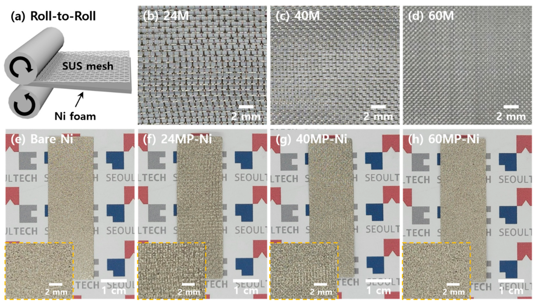
Figure 1a illustrates the simple method used in this study for forming uniform microgrid-patterns on Ni foams using an SUS mesh as a rigid stamp during roll-pressing. Notably, compared to other patterning methods (e.g., chemical etching, lithography, and laser patterning), our stamp micro-patterning has distinct advantages, such as continuity of the roll-to-roll-based process, pattern uniformity, economic feasibility, and the absence of extra equipment and product lines [20]. Moreover, the MP morphology of the Ni foam surface was effectively designed by differentiating the mesh size; that is, by employing 24, 40, and 60 standard mesh sizes (ASTM E11), as shown in Figure 1b–d. The mesh size is defined as the number of openings per square inch (1 in = 2.54 cm). As the mesh number increases, the number of openings increases, and the opening size decreases. In addition, the diameter of the mesh wires decreases with an increase in the mesh number. Therefore, the surface morphology of the Ni foam, including its microgrid size, number of microgrids, and width/depth of the dented vertical stripes, can be systematically varied by changing the mesh size. Figure 1e−h display the four types of Ni foams: bare Ni, 24MP-Ni, 40MP-Ni, and 60MP-Ni. Bare Ni does not have a specific surface pattern. In contrast, 24MP-Ni, 40MP-Ni, and 60MP-Ni exhibit uniform microgrid-patterns on their surfaces. The enlarged images of the different MP-Ni foams (inset images with orange dotted borders) revealed that these have a rough surface with prominent microgrid-patterns compared with the bare Ni foam with a smooth surface.
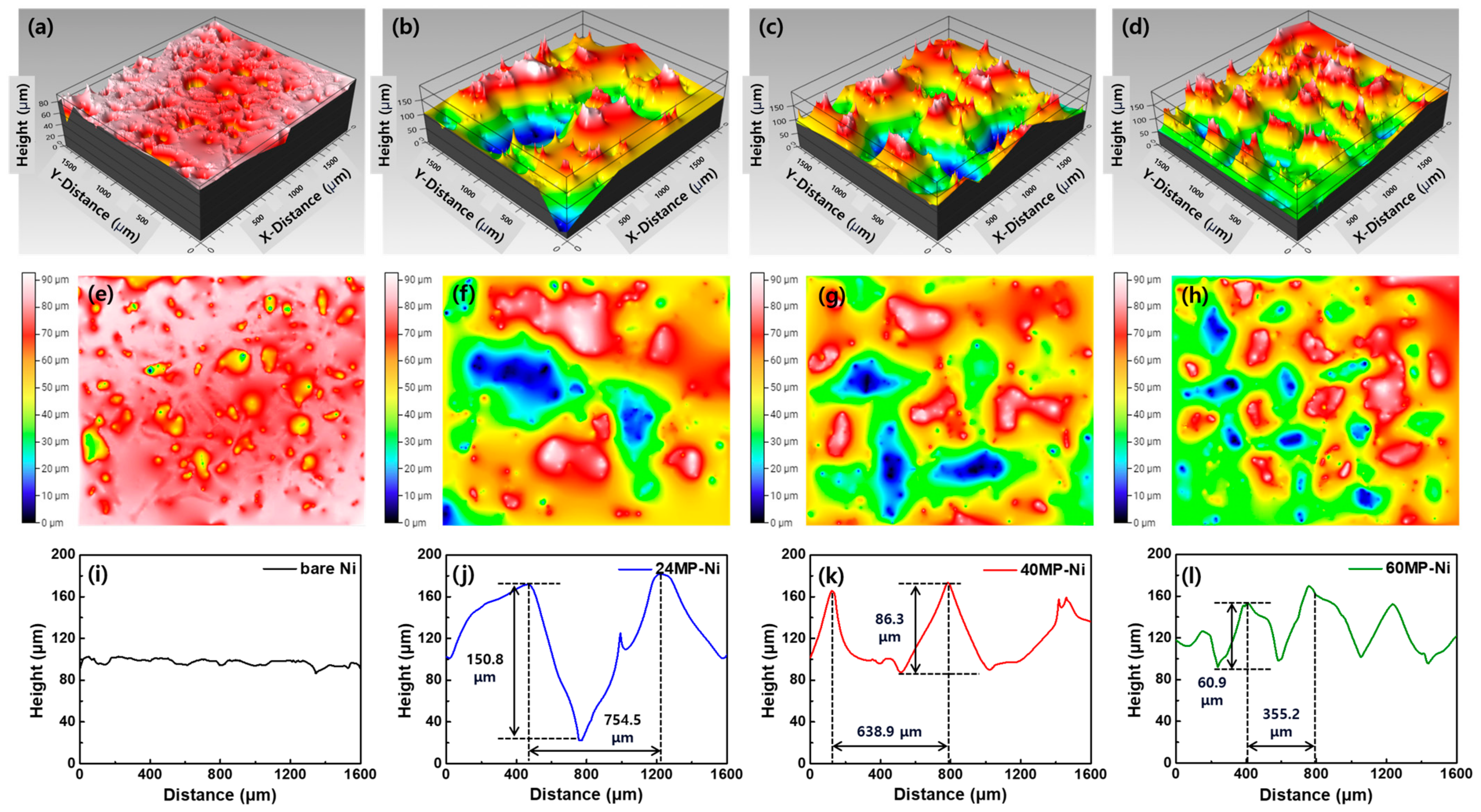
To investigate the MP morphology of the MP-Ni foams, their 3D microtopography images were obtained (Figure 2). As shown in the 3D image in Figure 2a, bare Ni had no specific micro-roughness; the slight surface roughness (<10 μm) is attributed to the inherent morphology of the foam itself. In contrast, the MP-Ni samples (24MP-Ni, 40MP-Ni, and 60MP-Ni) exhibited specific surface roughnesses, and their 3D topographic images presented protruding 3D microgrids of various scales and densities (Figure 2b−d). The density of the 3D microgrids increased, whereas the microgrid size decreased in the order of 24MP-Ni, 40MP-Ni, and 60MP-Ni. Figure 2e−l present the precise scales of the 3D microgrids of the Ni foams, as determined by 3D microtopography. Figure 2e−h show the top-view 2D roughness images of bare Ni, 24MP-Ni, 40MP-Ni, and 60MP-Ni, respectively, and Figure 2i−l show the corresponding line roughness data. Bare Ni exhibited no specific height variation within a height of 1600 μm from the sample surface, thus confirming its smooth surface morphology and the absence of a 3D micro-structure. In contrast, the MP-Ni samples exhibited specific height variations, confirming the formation of different 3D microstructures. The depth and width of the 3D microgrid-pattern decreased with increasing size of the mesh used for preparing Ni foam samples (150.8 and 754.5 μm for 24MP-Ni, 86.3 and 638.9 μm for 40MP-Ni, and 60.9 and 355.2 μm for 60MP-Ni, respectively), confirming that the surface roughness of the MP-Ni sample can be tuned simply by changing the mesh size. In summary, the 3D microtopography results of the bare Ni and MP-Ni foam samples confirm that the depths and widths of their surface features can be tuned.
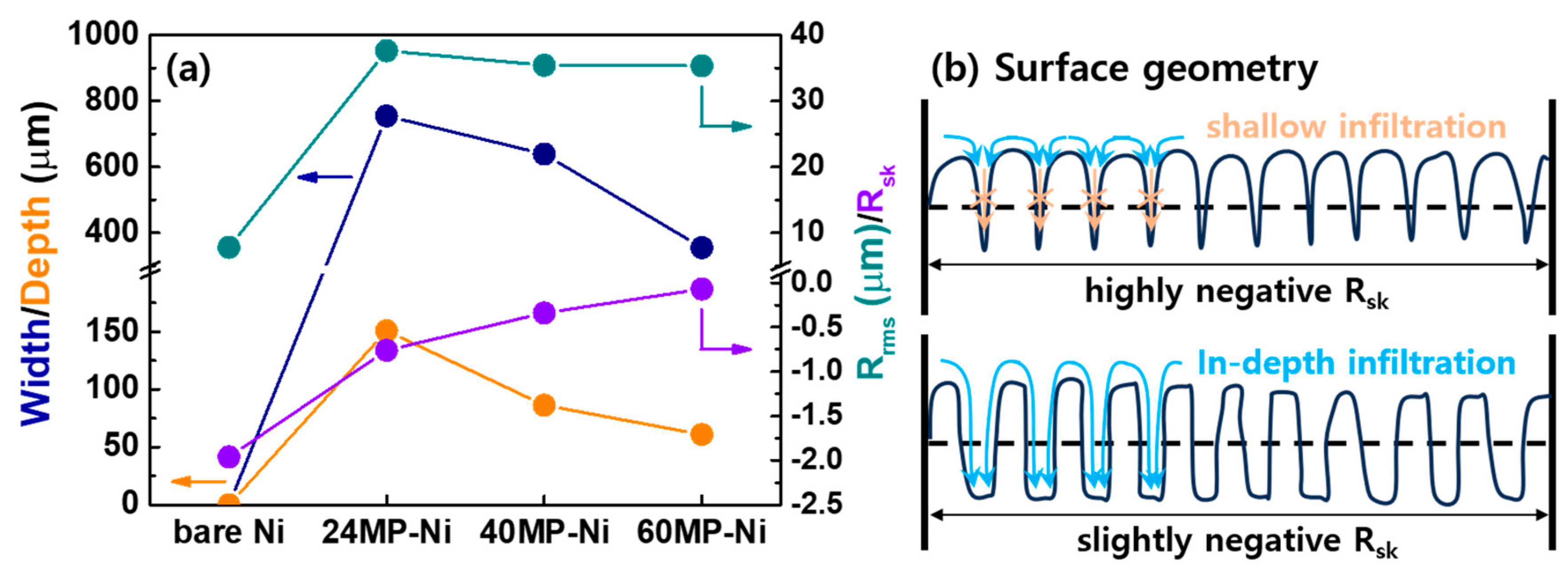
The surface geometry of each Ni sample was examined in terms of the width and depth of the 3D microgrid-pattern, root-mean-square roughness (Rrms), skewness roughness (Rsk), and the penetration depth of the active material (see Figure 3a and Table 1). Compared to bare Ni, all MP-Ni samples exhibited specific width and depth scales owing to their 3D microgrid-patterns, resulting in microscale surface roughness. Accordingly, all the MP-Ni samples had a higher Rrms value than the of bare Ni foam. A significant increase in the Rrms of the Ni foam results in its increased contact area with the active material layer, resulting in decreased interfacial resistance between the Ni foam current collector and active material. Consequently, the MP-Ni-based electrode accommodates (adsorbs/desorbs) a larger amount of charge during charge/discharge compared with that of the flat Ni foam-based electrode. Moreover, the Rsk value, defined as the asymmetry of the surface profile around its mean value, should be considered in describing the surface geometry obtained by 3D microgrid-patterning. As illustrated in Figure 3b, a highly negative Rsk represents a surface with predominantly sharp valleys, whereas a slightly negative Rsk represents a round surface with blunt valleys. Given that a viscous slurry mixture was used to cast the active layer, the surface geometry of the Ni foam with a highly negative Rsk induces shallow infiltration of the slurry mixture, creating voids between the active layer and Ni foam after drying [21]. These voids block electron transfer under ultrafast charge/discharge conditions and weaken the interfacial adhesion between the Ni foam and active material following repetitive charge/discharge cycles [22]. In comparison, the surface geometry of MP-Ni with a slightly negative Rsk facilitates deeper infiltration of the slurry mixture, leading to more complete contact between the active layer and Ni foam. Therefore, MP-Ni samples with slightly negative Rsk values (−0.46 for 24MP-Ni, −0.19 for 40MP-Ni, and −0.13 for 60MP-Ni) possibly enhance specific capacitance, even under high-rate charge/discharge conditions relative to that achieved using the bare Ni foam with a highly negative Rsk (−2.02). The gradual decrease in the Rsk in order of 24MP-Ni > 40MP-Ni > 60MP-Ni is attributed to the decrease in the mesh wire diameter, in accordance with the mesh size. This is because a smaller mesh diameter can alleviate the pressure exerted on the Ni foam during roll-pressing compared with that of a larger mesh diameter. Similarly, the width and depth of the 3D microgrid-pattern gradually decreased in the order of 24MP-Ni > 40MP-Ni > 60MP-Ni (Table 1). The surface geometry of the 3D MP-Ni foam is likely to affect the electron transfer characteristics of the active material layer, which is directly related to the charge adsorption/desorption kinetics and reversibility of the EDLC electrodes.
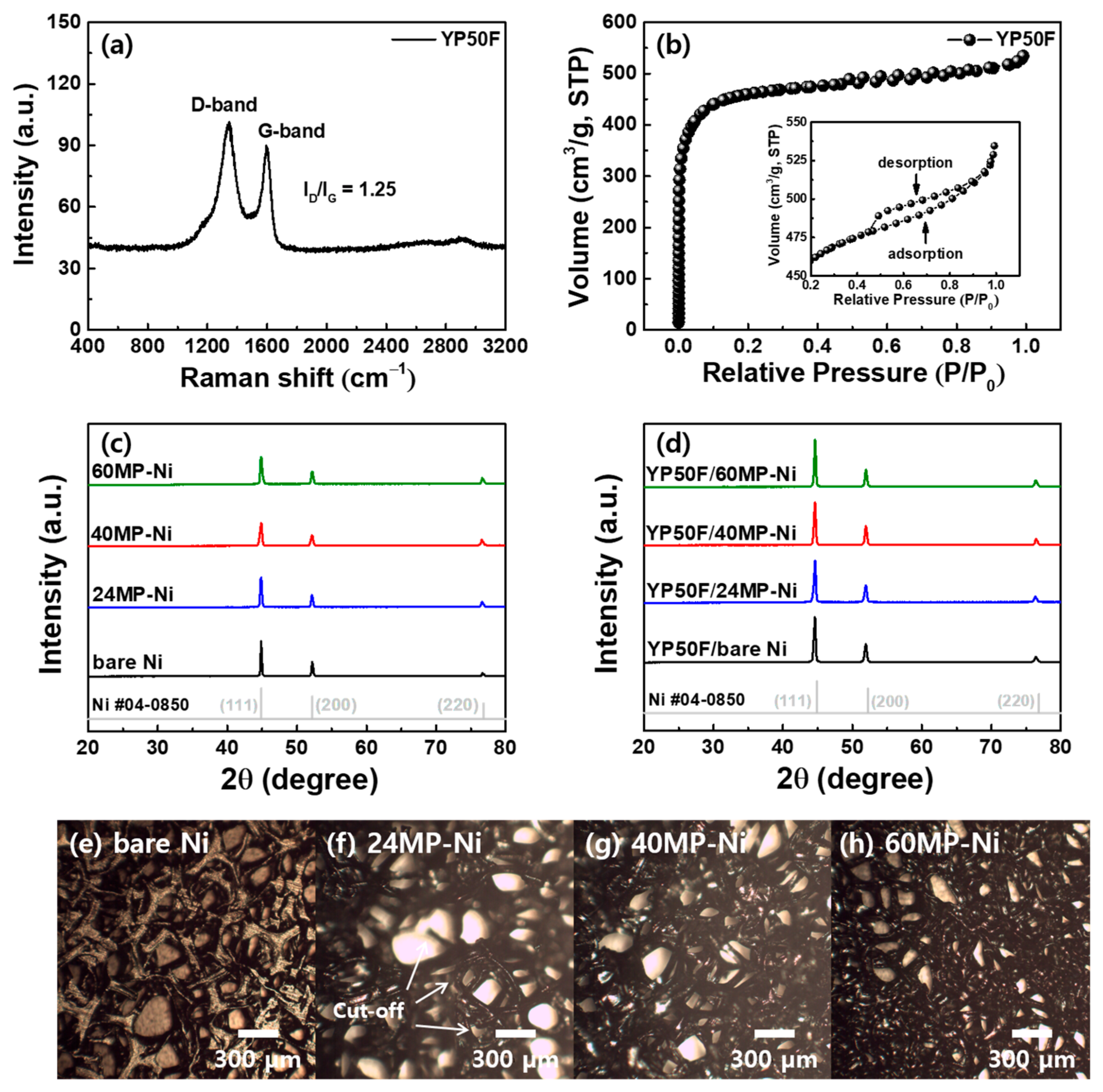
The Raman spectrum of the active material, YP50F, in Figure 4a exhibits broad peaks near 1341.5 and 1598.7 cm−1, corresponding to the D- and G-bands of carbon, respectively. Considering that the D-band of carbon originates from lattice defects, and the G-band is due to sp2-bonded carbon atoms, the high intensity ratio of the D- to G-band (ID/IG = 1.25) confirms the amorphous nature of the carbon material (i.e., YP50F) used in this study. Figure 4b shows the nitrogen adsorption/desorption curves of YP50F. In the low relative pressure range, the volume change curve shows a sharp change due to rapid nitrogen adsorption/desorption from the micropores. Further, the hysteresis loop in the relative pressure range of 0.2–1.0 indicates the presence of mesopores. The adsorption data reveal a specific surface area of 1760.9 m2/g of YP50F, indicating that it is a suitable active material for EDLC electrodes. Figure 4c presents the XRD patterns of bare Ni, 24MP-Ni, 40MP-Ni, and 60MP-Ni in the 2 θ range of 20−80°. All Ni foams exhibited common diffraction peaks at approximately 44.8°, 52.3°, and 76.7°, corresponding to the (111), (200), and (220) planes of Ni, respectively (JCPDS #04-0850) [23]. The XRD patterns of the MP-Ni samples without any peaks attributable to specific impurities or phase conversion confirmed the mild processability of the roll-to-roll mesh-patterning method. The XRD patterns of the EDLC electrodes prepared by casting the slurry of YP50F on the bare and MP-Ni foams (i.e., YP50F/bare Ni, YP50F/24MP-Ni, YP50F/40MP-Ni, and YP50F/60MP-Ni) were also analyzed (Figure 4d). Consistent with the XRD results of the Ni foam (Figure 4c), all electrodes yielded diffraction peaks at 44.5°, 51.9°, and 76.3° for Ni. Considering that YP50F has a highly porous and amorphous carbon structure, no specific diffraction peaks of carbon were observed. Figure 4e−h show the OM images of bare Ni, 24MP-Ni, 40MP-Ni, and 60MP-Ni, respectively. All Ni foams were found to have net-like morphology with a Ni wire diameter of 61.3−93.5 μm; this morphology facilitates a larger contact area with the active material layer and thus enhances electron transfer and adhesion compared with the case of the flat Ni foam. Notably, compared with the continuous foam morphology of the other Ni samples, 24MP-Ni revealed discontinuous Ni wires, which can be attributed to excessive pressure induced by the 24 mesh stamp with a larger mesh diameter during stamp micropatterning. The discontinuity of the Ni wires in 24MP-Ni is likely to inhibit facile electron transfer to the active material. On the contrary, 40MP-Ni and 60MP-Ni with a continuous net-like foam morphology allows the electrons to flow rapidly and uniformly toward the active material during ultrafast charge/discharge.
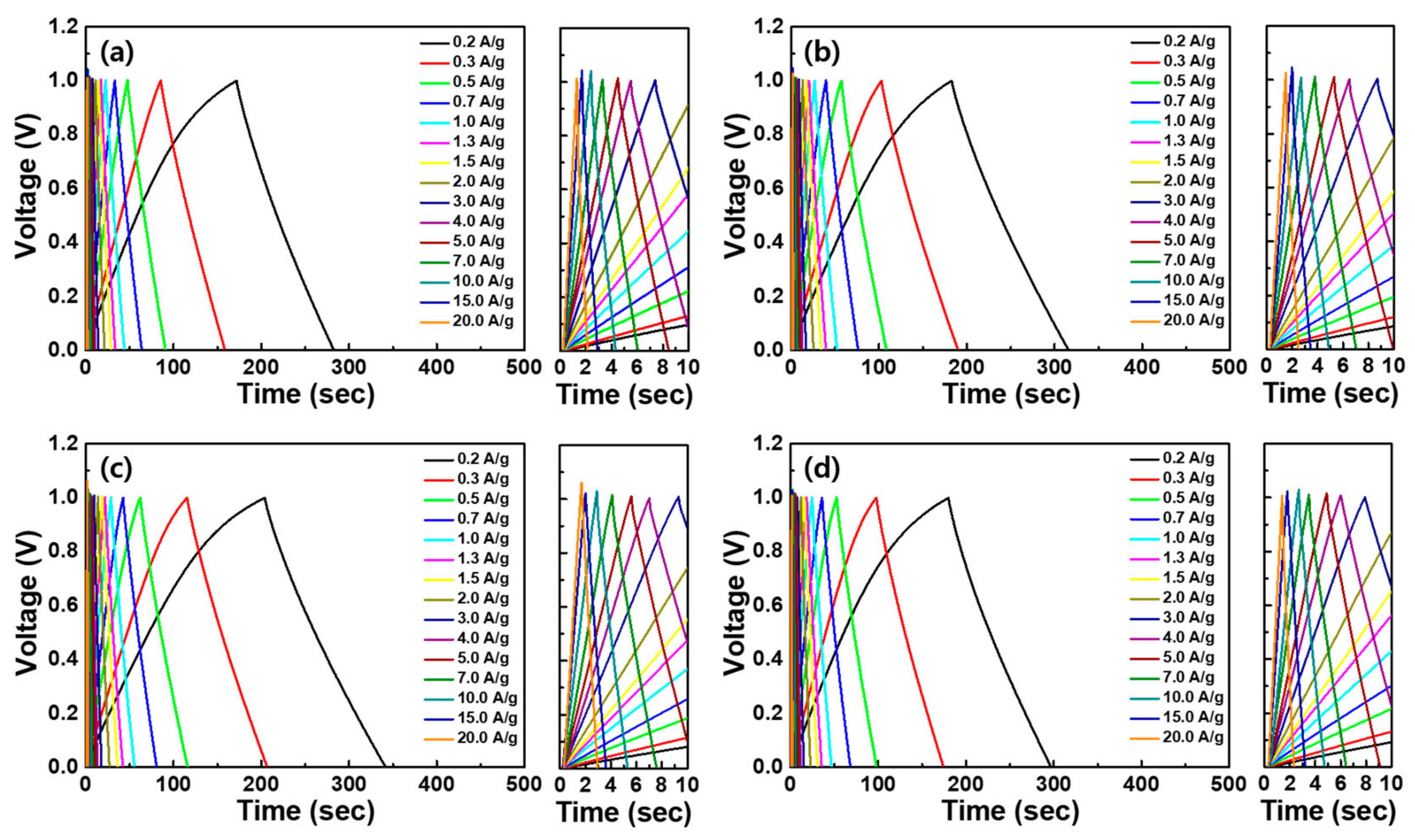
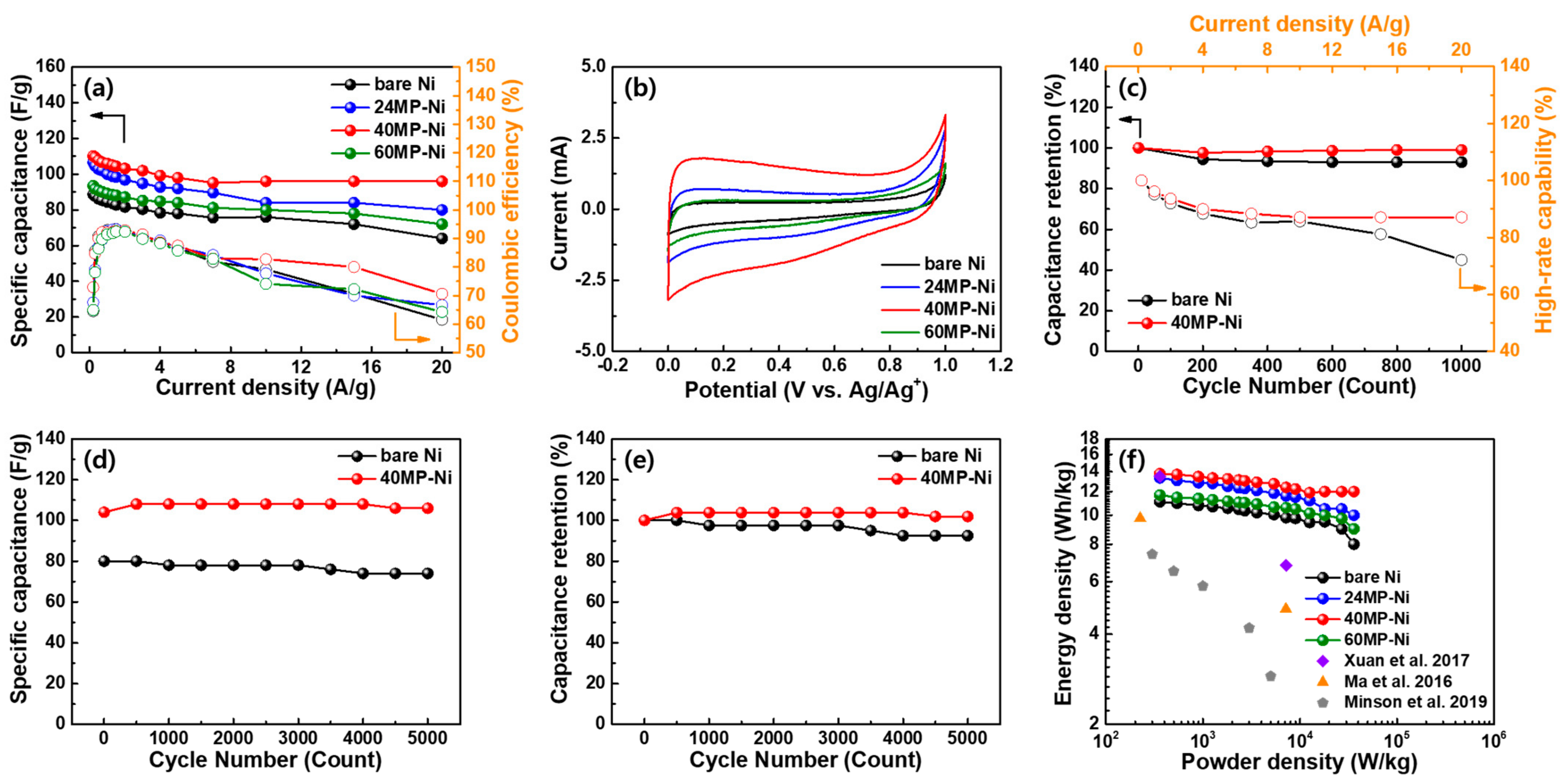
To evaluate the electrochemical performances of the EDLC electrodes fabricated using bare Ni, 24MP-Ni, 40MP-Ni, and 60MP-Ni as current collectors, their gravimetric charge–discharge curves and specific capacitances were evaluated at different current densities in the range of 0.2–20 A/g (Figure 5). All samples exhibited symmetric linear curves during charge/discharge, which is attributable to the physical adsorption/desorption-based charge transport mechanism of these EDLC electrodes. Among the samples, YP50F/40MP-Ni showed the longest charge–discharge times at all current densities. Based on the gravimetric charge–discharge data in Figure 5, the specific capacitances were calculated for all electrodes (see Figure 6a). Notably, the YP50F/MP-Ni samples had a higher specific capacitance than the YP50F/bare Ni sample at all current densities. The increased specific capacitances of the YP50F/MP-Ni samples can be attributed to the MP morphology of the Ni foam current collector, which promoted considerable electron transport to the active material layer, thus increasing the amount of charge adsorbed/desorbed during charge/discharge processes. More importantly, among the EDLC electrodes, YP50F/40MP-Ni showed exceptional specific capacitance retention, even at an ultrafast charge/discharge rate of 20 A/g. As summarized in Table 2, YP50F/40MP-Ni exhibited the greatest specific capacitance retention (87.1%) in the range of 0.2–20 A/g, followed by YP50F/60MP-Ni (77.0%), YP50F/24MP-Ni (75.0%), and YP50F/bare Ni (72.1%). Thus, YP50F/40MP-Ni exhibits ultrafast-rate capability because the Ni foam (40MP-Ni) facilitates electron transfer at its interface with the active carbon material, even under ultrafast charge/discharge conditions. The Coulombic efficiency (CE), defined as the ratio of the discharge capacity to charge capacity, indicates the charge adsorption/desorption reversibility during the charge–discharge processes. Considering that the charge storage mechanism of the EDLC electrode is based on the surface adsorption/desorption of charge pairs (electrons and electrolyte ions), the CE is significantly influenced by the electrical conductivity of the electrode. Thus, YP50F/40MP-Ni exhibited higher CE values than the other electrodes at all current densities, especially at ultrafast-rate current densities of 10, 15, and 20 A/g (Table 3). Figure 6b shows the CV profiles of bare Ni, 24MP-Ni, 40MP-Ni, and 60MP-Ni in the voltage range of 0–1 V. All Ni foam-based electrodes yielded a broad closed curve without specific redox peaks owing to the typical electrochemical behavior of the EDLC electrode. The absence of specific peaks in the CV curves indicates that the electrode does not undergo the Faradaic process—a common charge storage mechanism in PCs—in the applied voltage range. The CV curve areas of all the MP-Ni-based electrodes were larger than that of the bare Ni-based electrode, implying that the 3D MP interfacial geometry of the MP-Ni foams results in enhanced electrochemical activity with greater charge adsorption/desorption compared to that of the bare Ni foam. Remarkably, YP50F/40MP-Ni exhibited the largest CV curve area among the electrodes, thus indicating the highest electrochemical activity. This can be attributed to the optimized surface geometry of the MP-Ni foam, which leads to deep infiltration of the YP50F slurry, facilitating the full utilization of the active material/Ni foam interface. More importantly, the robust contact geometry and increased contact area at the active material/Ni foam interface enhanced the electrochemical reversibility of the system and promoted fast-rate charge transport during repetitive and ultrafast charge/discharge cycles. Figure 6c compares the capacitance retention and high-rate capability of YP50F/40MP-Ni with those of YP50F/bare Ni for different cycle numbers and current densities, respectively. YP50F/40MP-Ni exhibits a capacitance retention of 98.98% after 1000 consecutive charge/discharge cycles at 1 A/g, outperforming the YP50F/bare Ni electrode (92.99%). Furthermore, YP50F/40MP-Ni features a high-rate capability—defined as the specific capacitance retention at a given current density relative to that at 0.2 A/g—of 87.1% at 20 A/g, while YP50F/bare Ni exhibits an inferior high-rate capability of 72.1% at 20 A/g. To evaluate the ultrafast longevity of the MP-Ni-based EDLC electrodes, we compared the specific capacitance variations of the electrodes based on bare Ni and 40MP-Ni during 5000 consecutive charge/discharge cycles at 5 A/g (Figure 6d,e). YP50F/40MP-Ni showed a constant specific capacitance (106.0 F/g after 5000 cycles) with a superior retention of 101.9% compared with that of YP50F/bare Ni (specific capacitance of 74.0 F/g and retention of 92.5% after 5000 cycles). These results demonstrate the remarkable ultrafast longevity of 40MP-Ni as a current collector for EDLC electrodes. Figure 6f presents the energy density plots at power densities in the range of 360−36,000 W/kg for all Ni foam samples. The energy and power densities were calculated as follows:
Energy density = Specific capacitance × (dV)2/8,
Power density = Energy density/dt,
where dV and dt denote the potential window (V) and discharge time (s), respectively. YP50F/40MP-Ni presented a notably higher energy density of 12.0 Wh/kg even at a high power density of 36,000 W/kg compared with those of bare Ni (8.0 Wh/kg), 24MP-Ni (10.0 Wh/kg), and 60MP-Ni (9.0 Wh/kg) (Table 2). Furthermore, YP50F/40MP-Ni exhibited better energy storage capability at high power densities than those reported previously for other EDLCs [24,25,26]. Therefore, the evaluated energy storage performances demonstrated the improved charge transport behaviors of our electrodes, including an ultrafast kinetics, reversibility, and electrochemical activity, owing to the 3D MP surface geometry of the Ni foam current collector. In particular, the optimized surface geometry of 40MP-Ni with a slightly negative Rsk (−0.19) and high Rrms (35.4 μm) facilitates its complete adhesion to the active material and increases the contract area between the two, facilitating accelerated electron transfer during ultrafast and repetitive charge/discharge cycles.
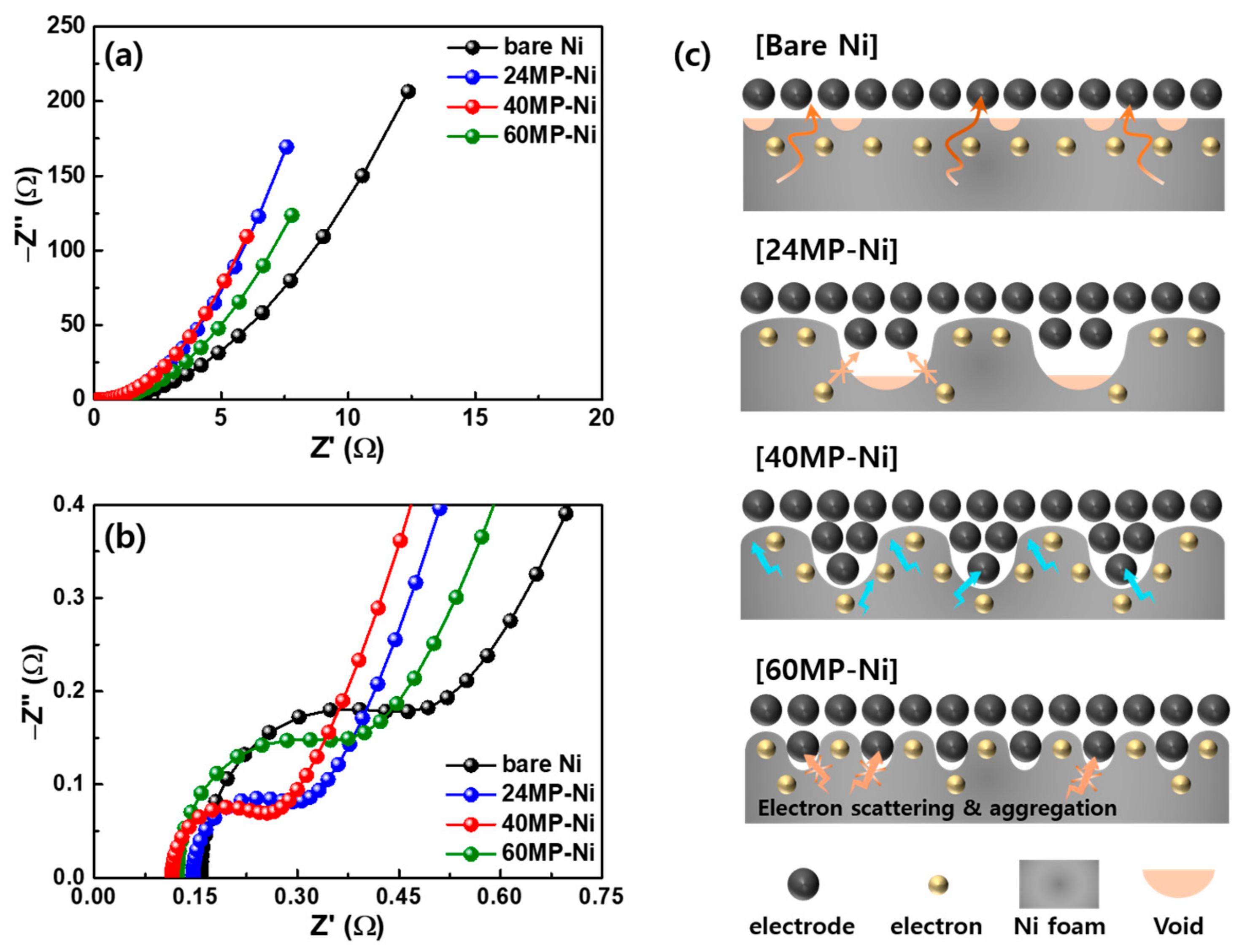
Figure 7a,b show the Nyquist plots of the EDLC electrodes based on bare Ni, 24MP-Ni, 40MP-Ni, and 60MP-Ni. EIS, represented as measured impedance plots in the applied frequency range, is considered a suitable tool to clarify the interfacial resistance of electrochemical electrodes. Typically, EIS results are categorized into two domains: (ⅰ) the low-frequency region, represented by a straight line, referred to as the Warburg impedance, and (ⅱ) the high-frequency region, represented by a semicircle [27]. The low-frequency region is dominated by ion diffusion resistance at the electrode/electrolyte interface, whereas the high-frequency region represents from electron transfer resistance across the electrode/electrolyte interface [28,29]. As shown in Figure 7a, YP50F/40MP-Ni exhibited the steepest slope with a value of 30.96 (YP50F/bare Ni: 20.35, YP50F/24MP-Ni: 25.86, and YP50F/60MP-Ni: 28.37), confirming that it has the lowest ion-diffusion resistance for electric double layer formation at the electrode/electrolyte interface [30,31]. Additionally, it exhibits the smallest semicircle with a charge transfer resistance of 0.128 Ω (YP50F/bare Ni: 0.293 Ω, YP50F/24MP-Ni: 0.142 Ω, and YP50F/60MP-Ni: 0.236 Ω), demonstrating the most active electron transfer across the electrode/electrolyte interface, as seen in the enlarged EIS profiles verifying the impedance plots in the high frequency region (Figure 7b). The extremely small semicircle (<1 Ω) implies a double layered charge storage mechanism based on the physical adsorption/desorption of charged species at the electrode/electrolyte interface for all electrodes [32]. The EIS result with a gentle slope and the largest semicircle for YP50F/bare Ni suggests the most resistive interfacial charge transport, owing to the absence of a specific surface geometry for the bare Ni foam. The scheme in Figure 7c illustrates the interfacial charge transport with cross-sectional views of all EDLC electrodes. Despite the smallest microscopic features of the patterned 60MP-Ni, a gentler slope and a larger semicircle were generated compared with those of 24MP-Ni and 40MP-Ni, indicating a higher interfacial charge transport resistance at the electrode/electrolyte interface. The degraded interfacial charge transport in 60MP-Ni can be attributed to the excessive contact area between the electrode and Ni foam, which possibly causes electron scattering and aggregation, leading to a fast-rate and inhomogeneous electron transfer [33]. Conversely, the relatively large microscopic features in 24MP-Ni can provide a relatively low contact area between the active material and Ni foam and more interfacial voids, preventing ultrafast electron transfer during high-rate charge/discharge [34]. Owing to its optimized surface geometry with a 3D microgrid-pattern, 40MP-Ni enhances charge transport toward ultrafast kinetics and reversibility even under an ultrafast-rate charge/discharge process through the following synergistic effects: (ⅰ) a significant increase in the Rrms increased its contact area with active material, thus accommodating considerable charge transfer during ultrafast charge/discharge process and thereby improving ultrafast-rate capability; (ⅱ) the slightly negative Rsk, which is almost zero, promotes deep infiltration of the carbon slurry, thus leading to rigid adhesion with minimized interfacial defects (voids and electron scatters) at the rough surface, encouraging reversible charge transport during repetitive fast-rate cycles. Owing to its rigid interface adhesion structure, the EDLC electrode fabricated using 40MP-Ni exhibited notable flexibility, especially under ultrafast charge/discharge conditions. 
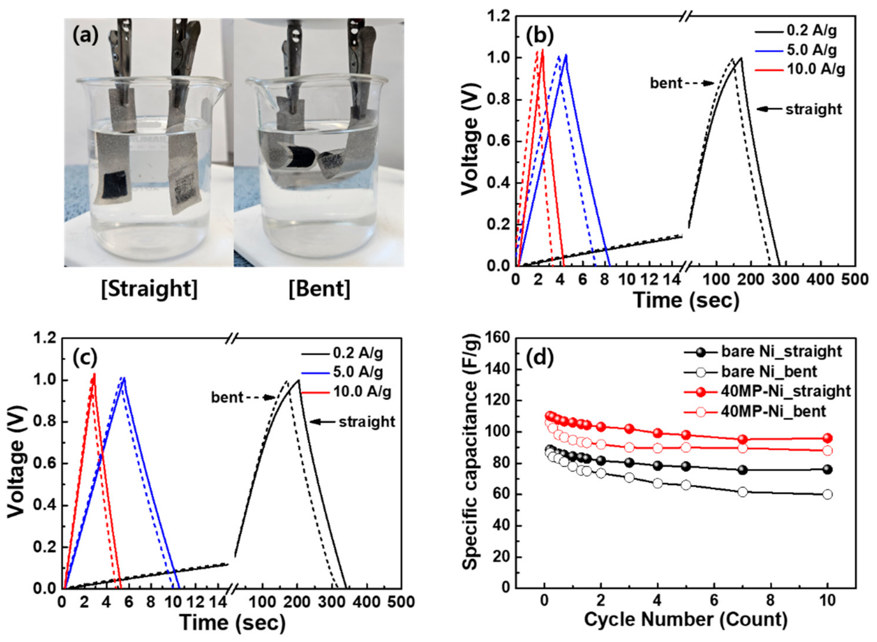
Figure 8a shows photographs of symmetric EDLC electrodes fabricated from 40MP-Ni in the straight and bent states, respectively. Based on the measurement conditions in Figure 8a, gravimetric charge–discharge curves of YP50F/bare Ni and YP50F/40MP-Ni were measured in the straight and bent states, respectively. YP50F/40MP-Ni exhibited excellent charge/discharge capability, even at 5 and 10 A/g (Figure 8c), whereas the YP50F/bare Ni electrode showed a significantly lower charge/discharge capability at 5 and 10 A/g (Figure 8b). Thus, YP50F/40MP-Ni delivered specific capacitances of 106.1, 90.0, and 88.1 F/g at 0.2, 5, and 10 A/g, respectively, which are comparable to those observed in the straight state (Figure 8d). However, the YP50F/bare Ni electrode showed specific capacitances of 86.6, 66.0, and 60.1 F/g at 0.2, 5, and 10 A/g, respectively, which are lower than those observed in the straight state. The 3D microgrid-patterns on the Ni foam current collector significantly enhanced the interfacial adhesion of the foam with the active material layer, enabling rapid electron transfer, even under ultrafast charge/discharge conditions.

4. Conclusions

Ni foams with tunable surface geometry were fabricated using different-sized SUS meshes as rigid stamps during roll pressing. The resulting Ni foam samples presented different width and depth scales of the 3D microgrid-patterns on their surfaces. The 3D MP morphologies of the Ni foams were effectively designed by adjusting the mesh scale to 24, 40, and 60 using SUS meshes of standard sizes. The MP-Ni with different surface geometries had different surface parameters, including Rrms, Rsk, and width/depth of the surface features. Among the three samples, 40MP-Ni had an optimal surface geometry, with a high Rrms (35.4 μm), slightly negative (near zero) Rsk (−0.19), and significantly high contact area with the active material (638.9 and 86.3 μm in width and depth, respectively). The Ni foam with the optimized 3D MP surface geometry enhanced the reversible charge transport kinetics of the EDLC electrode compared with that observed with the bare Ni foam. Accordingly, EDLC electrodes fabricated with 40MP-Ni as the current collector exhibited an ultrafast-rate capability (96.0 F/g at 20 A/g) and electrochemical reversibility (capacitance retention of 98.98% after 1000 consecutive charge/discharge cycles at 1 A/g). Designing the surface geometry of Ni foams (used as current collectors) via stamp micro-patterning can be an effective strategy to improve the ultrafast-rate capability of EDLC electrodes without requiring specific optimization of the active materials.

Author Contributions

Methodology, U.-T.K.; Data curation, U.-T.K.; Conceptualization, M.-H.J. and H.-J.A., Writing—original draft, M.-H.J., Writing—review and editing, H.-J.A. All authors have read and agreed to the published version of the manuscript.

Funding

This work was supported by the National Research Foundation of Korea (NRF) grant funded by the Korea government (MSIT) (RS-2023-00209244) and the Basic Science Research Program through the National Research Foundation of Korea (NRF) funded by the Ministry of Education (NRF-2021R1A6A1A03039981).

Data Availability Statement

The original contributions presented in the study are included in the article, further inquiries can be directed to the corresponding author.

Conflicts of Interest

The authors declare no conflicts of interest.

References

  1. Jeong, S.-J.; Jo, M.-H.; Ahn, H.-J. 3D-printed film architecture via automatic micro 3D-printing system: Micro-intersection engineering of V2O5 thin/thick films for ultrafast electrochromic energy storage devices. Chem. Eng. J. 2023, 475, 146503. [Google Scholar] [CrossRef]
  2. Jo, M.-H.; Jang, H.-N.; Ahn, H.-J. Oxygen-deficient cobalt vanadium oxide nano-planted mesoporous carbon nanofibers for ultrafast lithium-ion capacitors. J. Alloys Compd. 2023, 962, 171037. [Google Scholar] [CrossRef]
  3. Hussain, J.; Khan, A.; Zhou, K. The impact of natural resource depletion on energy use and CO2 emission in Belt & Road Initiative countries: A cross-country analysis. Energy 2020, 199, 117409. [Google Scholar] [CrossRef]
  4. Yadav, A.A.; Hunge, Y.M.; Liu, S.; Kulkarni, S.B. Ultrasound assisted growth of NiCo2O4@carbon cloth for high energy storage device application. Ultrason. Sonochem. 2019, 56, 290–296. [Google Scholar] [CrossRef] [PubMed]
  5. Kadam, V.S.; Jagtap, C.V.; Lokhande, P.E.; Bulakhe, R.N.; Kang, S.-W.; Yadav, A.A.; Pathan, H.M. One-step deposition of nanostructured Ni(OH)2/rGO for supercapacitor applications. J. Mater. Sci. Mater. Electron. 2023, 34, 1083. [Google Scholar] [CrossRef]
  6. Kumar, Y.A.; Yadav, A.A.; Al-Asbahi, B.A.; Kang, S.W.; Moniruzzaman, M. Sulfur nanoparticle-decorated nickel cobalt sulfide hetero-nanostructures with enhanced energy storage for high-performance supercapacitors. Molecules 2022, 27, 7458. [Google Scholar] [CrossRef] [PubMed]
  7. Chang, H.S.; Lee, B.-M.; Yun, J.M.; Choi, J.-H. Preparation and electrochemical characterization of porous carbon pearls from carboxymethyl cellulose for electrical double-layer capacitors. Korean J. Chem. Eng. 2022, 39, 1232–1239. [Google Scholar] [CrossRef]
  8. Yin, B.; Hao, L.; Wei, T.; Wang, C.; Zhu, B.; Li, X.; Yang, Q. Revealing bulk reaction kinetics of battery-like electrode for pseudocapacitor with ultra-high rate performance. Chem. Eng. J. 2022, 450, 138224. [Google Scholar] [CrossRef]
  9. Minakshi, M.; Higley, S.; Baur, C.; Mitchell, D.R.G.; Jones, R.T.; Fichtner, M. Calcined chicken eggshell electrode for battery and supercapacitor applications. RSC Adv. 2019, 9, 26981. [Google Scholar] [CrossRef]
  10. Minakshi, M.; Mitchell, D.R.G.; Jones, R.T.; Pramanik, N.C.; Jean-Fulcrand, A.; Garnweitner, G. A hybrid electrochemical energy storage device using sustainable electrode materials. ChemistrySelect 2020, 5, 1597–1606. [Google Scholar] [CrossRef]
  11. Lee, J.H.; Kang, Y.-M.; Roh, K.C. Enhancing gravimetric and volumetric capacitance in supercapacitors with nanostructured partially graphitic activated carbon. Electrochem. Commun. 2023, 154, 107560. [Google Scholar] [CrossRef]
  12. Wu, J. Understanding the electric double-layer structure, capacitance, and charging dynamics. Chem. Rev. 2022, 122, 10821–10859. [Google Scholar] [CrossRef] [PubMed]
  13. Udayakumar, M.; Tóth, P.; Wiinikka, H.; Malhotra, J.S.; Likozar, B.; Gyergyek, S.; Leskó, A.K.; Thangaraj, R.; Németh, Z. Hierarchical porous carbon foam electrodes fabricated from waste polyurethane elastomer template for electric double-layer capacitors. Sci. Rep. 2022, 12, 11786. [Google Scholar] [CrossRef]
  14. Daraghmeh, A.; Hussain, S.; Haq, A.U.; Saadeddin, I.; Servera, L.; Ruiz, J.M. Carbon nanocomposite electrodes for electrical double layer capacitor. J. Energy Storage 2020, 32, 101798. [Google Scholar] [CrossRef]
  15. Kim, S.-W.; Kim, I.-H.; Kim, S.-I.; Jang, J.-H. Nickel hydroxide supercapacitor with a theoretical capacitance and high rate capability based on hollow dendritic 3D-nickel current collectors. Chem. Asian J. 2017, 12, 1291–1296. [Google Scholar] [CrossRef] [PubMed]
  16. Liu, L.; Zhao, H.; Wang, Y.; Fang, Y.; Xie, J.; Lei, Y. Evaluating the role of nanostructured current collectors in energy storage capability of supercapacitor electrodes with thick electroactive materials layers. Adv. Funct. Mater. 2018, 28, 1705107. [Google Scholar] [CrossRef]
  17. ISO 25178-602:2010; Geometrical product specifications–Surface texture: Areal–Part 602: Nominal characteristics of non-contact (confocal chromatic probe) instruments. ISO: Geneva, Switzerland, 2010.
  18. Doberdò, I.; Löffler, N.; Laszczynski, N.; Cericola, D.; Penazzi, N.; Bodoardo, S.; Kim, G.-T.; Passerini, S. Enabling aqueous binders for lithium battery cathodes—Carbon coating of aluminum current collector. J. Power Sources 2014, 248, 1000–1006. [Google Scholar] [CrossRef]
  19. Jeong, H.; Jang, J.; Jo, C. A review on current collector coating methods for next- generation batteries. Chem. Eng. J. 2022, 446, 136860. [Google Scholar] [CrossRef]
  20. Choi, T.; Kim, S.J.; Park, S.; Hwang, T.Y.; Jeon, Y.; Hong, B.H. Roll-to-roll continuous patterning and transfer of graphene via dispersive adhesion. Nanoscale 2015, 7, 7138–7142. [Google Scholar] [CrossRef]
  21. Jeon, H.; Cho, I.; Jo, H.; Kim, K.; Ryou, M.-H.; Lee, Y.M. Highly rough copper current collector: Improving adhesion property between a silicon electrode and current collector for flexible lithium-ion batteries. RSC Adv. 2017, 7, 35681–35686. [Google Scholar] [CrossRef]
  22. Kim, B.H.; Staller, C.M.; Cho, S.H.; Heo, S.; Garrison, C.E.; Kim, J.; Milliron, D.J. High mobility in nanocrystal-based transparent conducting oxide thin films. ACS Nano 2018, 12, 3200–3208. [Google Scholar] [CrossRef]
  23. Liu, G.; Qin, Y.; Lyu, Y.; Chen, M.; Qi, P.; Lu, Y.; Sheng, Z.; Tang, Y. Low-crystalline β-Ni(OH)2 nanosheets on nickel foam with enhanced areal capacitance for supercapacitor applications. Chem. Eng. J. 2021, 426, 131248. [Google Scholar] [CrossRef]
  24. Xuan, H.; Lin, G.; Wang, F.; Liu, J.; Dong, X.; Xi, F. Preparation of biomass-activated porous carbons derived from torreya grandis shell for high-performance supercapacitor. J. Solid State Electrochem. 2017, 21, 2241–2249. [Google Scholar] [CrossRef]
  25. Ma, G.; Hua, F.; Sun, K.; Zhang, Z.; Feng, E.; Peng, H.; Lei, Z. Porous carbon derived from stalk for symmetric supercapacitors. RSC Adv. 2016, 6, 103508. [Google Scholar] [CrossRef]
  26. Misnon, I.I.; Zain, N.K.M.; Jose, R. Conversion of oil palm kernel shell biomass to activated carbon for supercapacitor electrode application. Water Biomass Valorization 2019, 10, 1731–1740. [Google Scholar] [CrossRef]
  27. Minakshi, M.; Wickramaarachchi, K. Electrochemical aspects of supercapacitors in perspective: From electrochemical configurations to electrode materials processing. Prog. Solid State Chem. 2023, 69, 100390. [Google Scholar] [CrossRef]
  28. Laschuk, N.O.; Easton, E.B.; Zenkina, O.V. Reducing the resistance for the use of electrochemical impedance spectroscopy analysis in materials chemistry. RSC Adv. 2021, 11, 27925. [Google Scholar] [CrossRef]
  29. Cristoforetti, A.; Rossi, S.; Deflorian, F.; Fedel, M. On the limits of the EIS low-frequency impedance modulus as a tool to describe the protection properties of organic coatings exposed to accelerated aging tests. Coatings 2023, 13, 598. [Google Scholar] [CrossRef]
  30. Charoen-amornkitt, P.; Pholauyphon, W.; Suzuki, T.; Tsushima, S. An approach to unify capacitance measurements of electric double layer capacitors using sinusoidal potential scan. J. Energy Storage 2023, 66, 107522. [Google Scholar] [CrossRef]
  31. Sha, L.; Lin, J.; Qi, R.; Song, Y. Low-frequency experimental method for measuring the electric double-layer capacitances of multi-cell electrolysis stacks based on equivalent circuit. J. Power Sources 2023, 579, 233263. [Google Scholar] [CrossRef]
  32. Mei, B.-A.; Munteshari, O.; Lau, J.; Dunn, B.; Pilon, L. Physical interpretations of Nyquist plots for EDLC electrodes and devices. J. Phys. Chem. C 2018, 122, 194–206. [Google Scholar] [CrossRef]
  33. Jo, M.-H.; Koo, B.-R.; Kim, K.-H.; Ahn, H.-J. Tailored interface stabilization of FTO transparent conducting electrodes boosting electron and Li ion transport for electrochromic energy-storage devices. Chem. Eng. J. 2022, 431, 134036. [Google Scholar] [CrossRef]
  34. Zhang, X.; Meng, W.J.; Meng, A.C. Chemical potential gradient induced formation of Kirkendall voids at the epitaxial TiN/MgO interface. Nanoscale 2023, 15, 13086. [Google Scholar] [CrossRef]
Figure 1. (a) Schematic illustration of the microgrid-patterning of Ni foams using SUS meshes of different mesh sizes: (b) 24 mesh, (c) 40 mesh, and (d) 60 mesh. Photographs of the resultant Ni foams: (e) bare Ni, (f) 24MP-Ni, (g) 40MP-Ni, and (h) 60MP-Ni.
Metals 14 00354 g001
Figure 2. 3D micro-topography images of the Ni foams fabricated by the microgrid patterning method: (a) bare Ni, (b) 24MP-Ni, (c) 40MP-Ni, and (d) 60MP-Ni. (eh) Top-view surface roughness images of Ni foams and (il) the corresponding line roughness profiles: (e,i) bare Ni, (f,j) 24MP-Ni, (g,k) 40MP-Ni, and (h,l) 60MP-Ni.
Metals 14 00354 g002
Figure 3. (a) Surface geometry parameters (i.e., the width, depth, root-mean-square roughness (Rrms), and skewness roughness (Rsk) of the Ni foams. (b) Illustration of the infiltration of the surfaces of Ni foams with a highly negative Rsk and slightly negative Rsk.
Metals 14 00354 g003
Figure 4. (a) Raman spectrum and (b) nitrogen adsorption/desorption curves of YP50F. XRD patterns of the (c) Ni foam samples and (d) YP50F/Ni electrodes. OM images of the Ni foams: (e) bare Ni, (f) 24MP-Ni, (g) 40MP-Ni, and (h) 60MP-Ni.
Metals 14 00354 g004
Figure 5. Galvanostatic charge–discharge curves of the Ni foam-based electrodes at different current densities: (a) YP50F/bare Ni, (b) YP50F/24MP-Ni, (c) YP50F/40MP-Ni, and (d) YP50F/60MP-Ni.
Metals 14 00354 g005
Figure 6. (a) Specific capacitance and CE plots according to the current density in the range of 0.2–20 A/g for all EDLC electrodes. (b) CV profiles of the Ni foam-based electrodes in the potential range of 0–1.0 V. (c) Capacitance retention and high-rate capability plots according to cycle number and current density, respectively. (d) Specific capacitance and (e) capacitance retention plots for 5000 charge/discharge cycles at 5.0 A/g. (f) Energy density vs. power density plots of the Ni foam EDLC electrodes prepared in this study and some previously reported EDLC electrodes [24,25,26].
Metals 14 00354 g006
Figure 7. (a) EIS profiles and (b) enlarged EIS views for the EDLC electrodes. (c) Schematic illustration of interfacial charge transport with cross-sectional views for all EDLC electrodes.
Metals 14 00354 g007
Figure 8. (a) Photographs of symmetric EDLC electrodes in the straight and bent states, and (b,c) gravimetric charge–discharge curves obtained at 0.2, 5, and 10 A/g for (b) bare Ni and (c) 40MP-Ni EDLC electrodes. (d) Specific capacitance plots according to the current density in the range of 0.2 to 10 A/g for bare Ni and 40MP-Ni EDLC electrodes.
Metals 14 00354 g008
Table 1. Surface features (width, depth, Rrms, and Rsk) of all Ni foams.
Width (μm)Depth (μm)Rrms (μm)Rsk
Bare Ni--7.8−2.02
24MP-Ni754.5150.837.6−0.46
40MP-Ni638.986.335.4−0.19
60MP-Ni355.260.935.3−0.13
Table 2. Summary of the specific capacitances and energy densities of the Ni foam-based EDLC electrodes.
Specific Capacitance at 0.2 A/g (F/g)Specific Capacitance
at 1 A/g (F/g)
Specific Capacitance at 20 A/g (F/g)Energy Density at 360 W/kg (Wh/kg)Energy Density at 36,000 W/kg (Wh/kg)
Bare Ni88.784.464.011.18.0
24MP-Ni106.6100.080.013.310.0
40MP-Ni110.2106.096.013.812.0
60MP-Ni93.589.272.011.79.0
Table 3. CE values at different current densities for the Ni foam-based EDLC electrodes.
CE at 0.2 A/g (%)CE at 1 A/g
(%)
CE at 10 A/g
(%)
CE at 15 A/g
(%)
CE at 20 A/g
(%)
Bare Ni64.5592.9579.1770.5961.54
24MP-Ni67.5892.5977.7870.0066.67
40MP-Ni72.9292.0182.7680.0070.59
60MP-Ni64.9491.3974.0772.2264.29
Disclaimer/Publisher’s Note: The statements, opinions and data contained in all publications are solely those of the individual author(s) and contributor(s) and not of MDPI and/or the editor(s). MDPI and/or the editor(s) disclaim responsibility for any injury to people or property resulting from any ideas, methods, instructions or products referred to in the content.

